EP0729243A2 - Dispositif de réception optique numérique - Google Patents
Dispositif de réception optique numérique Download PDFInfo
- Publication number
- EP0729243A2 EP0729243A2 EP96301276A EP96301276A EP0729243A2 EP 0729243 A2 EP0729243 A2 EP 0729243A2 EP 96301276 A EP96301276 A EP 96301276A EP 96301276 A EP96301276 A EP 96301276A EP 0729243 A2 EP0729243 A2 EP 0729243A2
- Authority
- EP
- European Patent Office
- Prior art keywords
- signal
- circuit
- amplifier
- output
- reset
- Prior art date
- Legal status (The legal status is an assumption and is not a legal conclusion. Google has not performed a legal analysis and makes no representation as to the accuracy of the status listed.)
- Withdrawn
Links
Images




Classifications
-
- H—ELECTRICITY
- H04—ELECTRIC COMMUNICATION TECHNIQUE
- H04B—TRANSMISSION
- H04B10/00—Transmission systems employing electromagnetic waves other than radio-waves, e.g. infrared, visible or ultraviolet light, or employing corpuscular radiation, e.g. quantum communication
- H04B10/60—Receivers
- H04B10/66—Non-coherent receivers, e.g. using direct detection
- H04B10/69—Electrical arrangements in the receiver
- H04B10/695—Arrangements for optimizing the decision element in the receiver, e.g. by using automatic threshold control
Definitions
- the present invention relates to a digital optical receiving apparatus.
- the present invention relates to a digital optical receiving apparatus applicable to a burst signal transmission in a passive optical network (PON), an optical transmission system or an optical EATHERNET communication system.
- PON passive optical network
- EATHERNET optical EATHERNET communication system
- an optical receiving apparatus which receives an arbitrary signal pattern is of a DC coupling type.
- Japanese Patent Application No. Hei 6-217404 (filed on September 12, 1994) discloses an example of a conventional DC coupling type optical receiving apparatus.
- Japanese Patent Laid Open Publication No. Hei 5(1993)-227104 discloses an example of a circuit construction of the optical receiving apparatus with which a signal having no offset is output from an opto-electric conversion element.
- an optical signal having a waveform containing a light component having a level which is not completely zero level and a light component having a level not lower than a predetermined level is input.
- Such offset optical signal waveform whose its low level does not become zero level is produced when the optical extinction ratio of the signal is degraded for such reason that a semiconductor laser as a transmission light source is preliminarily biased in order to reduce a delay of light emission thereof. Emission of light whose optical extinction ratio is degraded is cut off on a transmitter side in time periods other than a burst signal period such that such light emission does not affect other burst signals.
- the optical receiving apparatus detects a high level and a low level of the received optical signal and obtains an optical receiving signal waveform using an intermediate level between the high and low levels of the received signal as a reference.
- the optical receiving signal in low level is not completely in zero level, the above-mentioned reference is deviated.
- the duty cycle of the waveform is determined by using the deviated reference, there may a case where the duty cycle detected is large in appearance.
- the degradation of duty cycle causes a data discriminating margin to be substantially degraded particularly when the receiving signal level is low.
- the degradation of data discriminating margin causes a minimum optical receiving level of the receiving circuit to be degraded.
- the reduction of the output signal amplitude of the ATC circuit leads to degradation of the minimum optical receiving level and reduction of dynamic range of the receiving circuit.
- the reduction of dynamic range results in a reduction of a system margin.
- An aim of at least the preferred embodiments of the present invention is to provide a digital optical receiving circuit with which a duty cycle variation of an output waveform of the circuit due to offset of an input signal and a degradation of signal amplitude can be minimized.
- a digital optical receiving circuit comprises:
- the amplifier means comprises a differential type pre-amplifier
- the threshold control means comprises an automatic threshold control circuit
- the reset means comprises a self-reset circuit for resetting a charge on a capacitance of said automatic threshold control circuit on the basis of the first or second signal.
- the self-reset circuit when the self-reset circuit detects that a level of the first or second signal output from the differential type pre-amplifier becomes equal to or higher than a predetermined level above an optical zero level, the self-reset circuit outputs a reset signal to reset the peak holding capacitor of the automatic threshold control circuit, so that the zero level of the offset optical signal is exactly held to thereby obtain an exact logic signal.
- the automatic threshold control circuit comprises a first peak holding circuit for holding a peak value of the first signal of positive phase output from the differential type pre-amplifier, a second peak holding circuit for holding a peak value of the second signal of inverted phase output from the differential pre-amplifier, a first adder for producing a first logical decision signal by adding the first signal of positive phase from the differential pre-amplifier and an output signal of the second peak holding circuit and a second adder for producing a second logical decision signal by adding the second signal of inverted phase from the differential type pre-amplifier and an output signal of the first peak holding circuit.
- the automatic threshold control circuit produces the first logical decision signal from the peak value of the signal from the second peak holding circuit and the first signal and the second logical decision signal from the peak value of the output signal of the first peak holding circuit and the second signal.
- the self-reset circuit includes a level detector, a reset pulse generator and a reset circuit.
- the level detector detects at least one of the first and second signals output from the differential type pre-amplifier which is equal to or higher than a predetermined level. Further, the self-reset circuit generates the reset pulse on the basis of the output signal of the level detector.
- the self-reset circuit outputs the reset signal for resetting the second peak holding circuit in the automatic threshold control circuit in order to hold the zero level of the optical signal when the output signal of the differential type pre-amplifier is equal to or higher than a certain constant level. With the second peak holding circuit being reset, the latter circuit becomes ready for operation.
- the reset circuit discharges the capacitor of the second peak holding circuit in the automatic threshold control circuit on the basis of the output signal of the reset pulse generator.
- the digital optical receiving circuit comprises an opto-electric conversion element, a differential type pre-amplifier, a first peak holding circuit, a second peak holding circuit, a first adder, a second adder, an automatic threshold control circuit, a comparator, a level detector, a reset pulse generator and a self-reset circuit.
- the differential type pre-amplifier amplifies an electric signal from the opto-electric conversion element to a predetermined level and outputting it as a first signal and a second signal.
- the first peak holding circuit holds a peak value of the first signal from the differential type pre-amplifier.
- the second peak holding circuit holds a peak value of the second signal from the differential pre-amplifier.
- the first adder produces a first logical decision signal by adding the first signal from the differential pre-amplifier and an output signal of the second peak holding circuit.
- the second adder produces a second logical decision signal by adding the second signal from the differential type pre-amplifier and an output signal of the first peak holding circuit.
- the automatic threshold control circuit is composed of the first and second peak holding circuits and the first and second adders.
- the comparator produces a logic signal on the basis of the first and second logical decision signals from the automatic threshold control circuit.
- the level detector determines whether or not at least one of the first and second signals from the differential type pre-amplifier exceeds a predetermined value.
- the reset pulse generator generates a reset pulse on the basis of an output of the level detector.
- the self-reset circuit includes a reset circuit for discharging the holding capacitor of the second peak holding circuit by the reset pulse from the reset pulse generator.
- the self-reset circuit detects that the first or second signal from the differential type pre-amplifier becomes equal to or higher than a certain constant level. When it is equal to or higher, the self-reset circuit generates the reset signal to reset the peak holding capacitor in the automatic threshold control circuit to thereby hold the zero level of the offset optical signal, resulting in an exact logic signal.
- the first adder includes a first resistor having one end connected to the output of the second peak holding circuit and a second resistor having one end connected to one of the output terminals of the differential type pre-amplifier. The other ends of the first and second resistors are connected commonly to one of the input terminals of the comparator.
- the second adder includes a third resistor having one end connected to the output of the first peak holding circuit and a fourth resistor having one end conected to the other output terminal of the differential pre-amplifier. The other ends of the third and fourth resistors are commonly connected to the other input terminal of the comparator.
- an anode of an opto-electric conversion element 101 is connected to a pre-amplifier 103 and a cathode thereof is connected to a bias source.
- the amplifier 103 is constructed with a differential amplifier 131 and resistors 132 and 133.
- An output of the amplifier 103 is connected to an input terminal of an automatic threshold control (ATC) circuit 105.
- the automatic threshold control circuit 105 is constructed with a first peak holding circuit 151, a second peak holding circuit 152 and resistors 153, 154, 155 and 156.
- An output of the ATC citcuit 105 is connected to one of input terminals of a comparator 107.
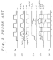
- Fig. 2 is a time chart showing a normal operation of the optical receiving circuit and Fig. 3 is a time chart showing an abnormal operation of the optical receiving circuit.
- abscissa is a time axis and (a) shows a burst signal, (b) an output waveform of the pre-amplifier, (c) an output waveform of the peak holding circuit and (d) an output signal waveform of the comparator.
- the optical receiving circuit is in a signal waiting state in which peak holding capacitors of the peak holding circuits 151 and 152 are discharged.
- the differential signals S bp and S bm are input to the ATC circuit 105 composed of the peak holding circuits 151 and 152 and the adders composed of the resistors 152 to 156.
- the signals S bp and S bm are produced such that a discriminating value L s used in the ATC circuit 105 to discriminate between a logic "1" and a logic "0" is set to an intermediate value between the signals S dp and S dm .
- the output signals S dp and S dm of the ATC circuit 105 which are shown in Fig. 2(d) are supplied to the comparator 107. In the comparator 107, these signals are converted into a signal S e composed of logic values "1" and "0" shown in Fig. 2(e).
- This optical signal has a waveform having optical quenching ratio degraded for the reason of preliminary biasing of a semiconductor laser as a transmission light source to reduce delay of light emission of the semiconductor laser.
- Light emission due to degradation of optical quenching ratio is cut off on a transmitter side in time periods other than a burst signal period such that such light emission does not affect other burst signals.
- the peak holding circuit 152 can not hold a level (-V L ) corresponding to the logic "0" of the second signal S bm of the pre-amplifier 103 exactly. Therefore, the peak holding circuit 152 continues to hold the value in the signal waiting state before the burst signal arrives thereat.
- the output of the ATC circuit 105 becomes a signal S dp whose level on the positive phase side varies between (V L + V S )/2 and (V L /2) and a signal S dm whose level on the inverted phase side varies between (V s )/2 and (0) as shown in Fig. 3(d) and thus the positive phase output S dp and the inverted phase output S dm become unbalanced in level.
- the comparator 107 outputs the signal S e having a different duty cycle and composed of logic values "0" and logic values "1". As a result, the amplitude of the output signal (logical decision signal) of the ATC circuit 105 is reduced.
- This degradation of the duty cycle causes the data discriminating margin to be degraded particularly when the receiving signal level is low. With such degraded margin of the data discrimination, the minimum light receiving level of the receiving circuit is degraded.
- the conventional optical receiving apparatus handling a burst data generally extracts, in order to achieve the high speed pull-in operation, the operation timing on the basis of information of both the rising edge and the falling edge of the data. Therefore, when the duty cycle is varied, the jitter of the extracted clock may be increased and the pull-in characteristics may be degraded.
- the reduction of the output signal amplitude leads to a reduction of the minimum light receiving level and a reduction of the dynamic range.
- the reduction of synamic range leads to a reduction of the system margin.
- a digital optical receiving circuit of the present invention which solves the above-mentioned problems, will be described in detail.
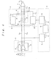
- Fig. 4 shows, in a block form, a construction of an embodiment of the digital optical receiving circuit of the present invention.
- respective components of the digital optical receiving circuit of the present invention are DC-coupled to each other.
- the digital optical receiving circuit of the present invention is generally constructed with an opto-electric conversion element 1, a differential type pre-amplifier 3, an automatic threshold control (ATC) circuit 5, a comparator 7 and a self-reset circuit 9.
- ATC automatic threshold control
- an anode of the opto-electric conversion element 1 is connected to the pre-amplifier 3 and a cathode thereof is connected to a bias source which is not shown.
- the pre-amplifier 3 is a transimpedance type differential amplifier composed of a differential amplifier 31 and feedback resistors 32 and 33.
- a positive phase output of the differential amplifier 31 is feedback to an inverted phase input thereof through the feedback resistor 33.
- an inverted phase output of the differential amplifier 31 is feedback to a positive phase input thereof through the feedback resistor 32.
- a first and second signals S bp and S bm from the pre-amplifier 3 are supplied to respective input terminals of the ATC circuit 5. The first signal is also supplied to the self-reset circuit 9.
- the ATC circuit 5 is constructed with a first peak holding circuit 51, a second peak holding circuit 52, a first adder circuit 58 composed of resistors 53 and 56 and a second adder circuit 57 composed of resistors 54 and 55.
- a logic decision signal for deciding a logic "1" or "0" can be set to an intermediate value of the amplitudes of the first and second output signals of the pre-amplifier 3.
- a positive phase output (first logical decision signal) of the ATC circuit 5 is obtained as a sum of the positive phase output of the pre-amplifier 3 and an output of the second peak holding circuit 52 which holds a peak value of the inverted phase output of the pre-amplifier 3.
- An inverted phase output of the ATC circuit 5 is obtained as a sum of the inverted phase output of the pre-amplifier 3 and an output of the first peak holding circuit 51 which holds a peak value of the positive phase output of the pre-amplifier 3.
- the respective outputs of the ATC circuit 5 are supplied to respective input terminals of the comparator circuit 7.
- the self-reset circuit 9 is constructed with a level detector 91 for detecting a signal in the output of the pre-amplifier 3, a reset pulse generator circuit 92 for generating a single pulse, reset signal in response to the signal detected by the level detector circuit 91 and a reset circuit 93 for discharging a hold capacitor of the second peak holding circuit 52 in response to the reset signal.
- Fig. 4 a timing chart of the operation shown in Figs. 5(a) to 5(g) having abscissa commonly showing time, in which Fig. 5(a) shows a burst signal, Fig. 5(b) shows an output waveform of the pre-amplifier, Fig. 5(c) shows an output waveform of the peak holding circuit and Fig. 5(d) shows an output waveform of the comparator.
- the burst signal shown in Fig. 5(a) is input to the digital optical receiving circuit which is in a waiting state with the holding capacitors of the peak holding circuits being discharged. Further, it should be remembered that the quenching ratio of the burst signal is degraded for the reasons of such as preliminary biasing of a semiconductor laser as a transmission light source to reduce the delay of light emission of the semiconductor laser.
- the assumption corresponds to a case where, in order to prevent the light emission with degraded quenching ratio from affecting other burst signals, the light emission is cut off on a transmitter side in other time than a time in which the burst signal exists.
- the optical signal S a When such optical signal S a is input to the opto-electric conversion element 1, the optical signal is amplified to a predetermined level by the pre-amplifier 3.
- the first signal S bp of the pre-amplifier 3 which is of a positive phase has a level (+V L ) as zero level and a level [+(V L +V S )] as peak level and the second signal S bm of the pre-amplifier 3 which is of an inverted phase has a level (-V L ) as zero level and a level [-(V L +V S )] as peak level, as shown in Fig. 5(b).
- the reset signal S d which is used to discharge the holding capacitor of the second peak holding circuit 52 is generated in a manner described below.
- the output signal S c of the level detector 91 becomes logic "1" simultaneously with the reception of the signal S a , as shown in Fig. 5(c).
- This signal S c is supplied to the reset pulse generator 92 from which a single pulse R d shown in Fig. 5(d) is obtained.
- the single pulse R d is input to the reset circuit 93, the latter circuit causes the holding capacitor of the second peak holding circuit 52 to be discharged.
- an output signal S ep of the first peak holding circuit 51 is continuously held at the peak level of the signal S bp which is the level +(V L +V S ) and an output signal S em of the second peak holding circuit 52 is held at the zero level (-V L ) of the signal S bm .
- the peak hbld values S ep and S em and the positive and inverted phase signals S bp and S bm from the pre-amplifier 3 are added in the first adder 58 and the second adder 57, respectively.
- logical decision signals S fp and S fm shown in Fig. 5(f) are produced as the output voltages of the ATC circuit 5.
- the discriminating value L s becomes a half value of the signal amplitude.
- the logical decision signals S fp and S fm are compared with the discriminating value by the comparator 7, resulting in a normalized output signal S g which takes logic "1" or "0" level as shown in Fig. 5(g).
- the self-reset circuit 9 is constructed with the level detector 91, the reset pulse generator 92 and the reset circuit 93.
- the level detector 91 is composed of a comparator 201 and an RS flip-flop 202.
- the output signal of the pre-amplifier 31 shown in Fig. 4 is input to a plus (+) terminal of the comparator 201 and a reference voltage V 1 is supplied to a minus (-) terminal thereof.
- the comparator 201 outputs a signal waveform S1.
- the latter signal is supplied to one input of the RS flip-flop 202 and a reset signal S2 is supplied to the other input of the flip-flop 202.
- the flip-flop 202 outputs a signal waveform S3.
- the signal S3 is supplied to the reset pulse generator 92 which composed of a delay circuit 203 and an Exclusive-OR circuit 204.
- the signal S3 is directly supplied to one input of the Exclusive-OR gate 204 and indirectly to the other input thereof through the delay circuit 203 as a signal S4 which is delayed from the signal S3 by a constant time.
- the Exclusive-OR gate 204 outputs a pulse signal S5.
- the pulse signals S2 and S5 are ORed by an OR circuit 205 of the reset circuit 93, resulting in a signal S6 which is supplied to a base of a transistor 206 of the reset circuit 93.
- An output of the transistor 206 that is, an output of the reset circuit 93, is supplied to the peak holding circuit 52 and held in a capacitor 210 thereof by charging the latter with the signal S bm from the pre-amplifier 3.
- the peak holding circuit 52 is composed of a comparator 207 and the capacitor 210, etc., and the charge of the capacitor 210 is discharged in response to the reset signal S6.
- the self-reset circuit 9 and the peak holding circuit 52 may be constructed in any of other known circuit constructions, respectively.
- the peak holding circuits hold the level of logic "1" or "0" of the signal exactly. Therefore, the degradation of duty cycle of the output waveform and the reduction of the output signal amplitude due to offset of the input signal and/or the pre-amplifier are minimized. Further, there are no degradation of system margin, no increase of jitter of the extracted clock and no degradation of the pull-in characteristics. Further, since the reduction of the output signal amplitude is minimized, there is substantially no degradation of the minimum receiving level and no reduction of the dynamic range in which optical signals are receivable.
- the peak hold circuits can hold the level of logic "1" and "0" of the signal exactly, the degradation of duty cycle of the output waveform and the reduction of the output signal amplitude due to offset of the input signal and/or the pre-amplifier are minimized. Further, there are no degradation of system margin, no increase of jitter of the extracted clock and no degradation of the pull-in characteristics.
- the peak value of the signal from the pre-amplifier is reliably held in the second peak holding circuit of the automatic threshold control circuit and can reliably discharge the holding capacitor of the second peak holding circuit, resulting in an exact peak holding characteristics.
- An output signal of an opto-electric conversion element 1 is amplified by a differential type pre-amplifier 3 to a predetermined level and input to an ATC circuit 5 as a positive phase signal and an inverted phase signal. These signals are held in respective peak holding circuits 51 and 52 of the ATC circuit.
- the positive phase signal held in the peak holding circuit 51 is added by an adder 57 to the inverted phase signal from the pre-amplifier 3 and the inverted phase signal held in the peak holding circuit 52 is added by an adder 58 to the positive phase signal from the pre-amplifier 3.
- Resultant sum signals are compared by a comparator with a reference and discriminated as logical "1" and "0".
- the positive phase signal from the pre-amplifier is input to a self-reset circuit 9 including a level detector 91, a reset pulse generator and a reset circuit 93.
- the level detector 91 detects a signal from the pre-amplifier 3.
- the reset pulse generator 92 generates a reset signal in the form of a single pulse by using an output of the level detector 91.
- the reset circuit 93 uses the reset signal to discharge a holding capacitor of the peak holding circuit 52. Degradation of duty cycle and of signal amplitude due to offset of an input signal can be minimized.
Landscapes
- Physics & Mathematics (AREA)
- Electromagnetism (AREA)
- Engineering & Computer Science (AREA)
- Computer Networks & Wireless Communication (AREA)
- Signal Processing (AREA)
- Optical Communication System (AREA)
- Dc Digital Transmission (AREA)
- Manipulation Of Pulses (AREA)
Applications Claiming Priority (2)
| Application Number | Priority Date | Filing Date | Title |
|---|---|---|---|
| JP36722/95 | 1995-02-24 | ||
| JP3672295 | 1995-02-24 |
Publications (2)
| Publication Number | Publication Date |
|---|---|
| EP0729243A2 true EP0729243A2 (fr) | 1996-08-28 |
| EP0729243A3 EP0729243A3 (fr) | 1998-04-22 |
Family
ID=12477648
Family Applications (1)
| Application Number | Title | Priority Date | Filing Date |
|---|---|---|---|
| EP96301276A Withdrawn EP0729243A3 (fr) | 1995-02-24 | 1996-02-26 | Dispositif de réception optique numérique |
Country Status (2)
| Country | Link |
|---|---|
| US (1) | US5822104A (fr) |
| EP (1) | EP0729243A3 (fr) |
Cited By (4)
| Publication number | Priority date | Publication date | Assignee | Title |
|---|---|---|---|---|
| GB2328816A (en) * | 1997-08-30 | 1999-03-03 | Siemens Plc | Optical data communications receiver |
| EP0735707A3 (fr) * | 1995-03-31 | 2000-03-01 | Kabushiki Kaisha Toshiba | Récepteur et émetteur-récepteur pour un signal numérique à forme arbitraire |
| EP1357717A1 (fr) * | 2002-04-25 | 2003-10-29 | Samsung Electronics Co., Ltd. | Dispositif pour commande automatique de seuil de décision pour récepteur optique en mode rafale |
| EP0981197A4 (fr) * | 1998-03-13 | 2005-03-30 | Matsushita Electric Industrial Co Ltd | Circuit amplificateur, et recepteur optique equipe de ce circuit |
Families Citing this family (24)
| Publication number | Priority date | Publication date | Assignee | Title |
|---|---|---|---|---|
| US5875050A (en) * | 1997-03-14 | 1999-02-23 | Lucent Technologies Inc. | Burst mode digital optical receiver |
| JP3031326B2 (ja) * | 1998-02-19 | 2000-04-10 | 日本電気株式会社 | バースト受信回路およびバースト受信回路の制御方法 |
| US6175438B1 (en) * | 1998-03-18 | 2001-01-16 | Lucent Technologies, Inc. | Differential optical signal receiver |
| JP2002164855A (ja) * | 2000-11-29 | 2002-06-07 | Oki Electric Ind Co Ltd | 光受信回路 |
| US7605649B2 (en) * | 2001-03-13 | 2009-10-20 | Marvell World Trade Ltd. | Nested transimpedance amplifier |
| US7551024B2 (en) * | 2001-03-13 | 2009-06-23 | Marvell World Trade Ltd. | Nested transimpedance amplifier |
| US7276965B1 (en) | 2001-03-13 | 2007-10-02 | Marvell International Ltd. | Nested transimpedance amplifier |
| JP2003264504A (ja) * | 2002-03-07 | 2003-09-19 | Oki Electric Ind Co Ltd | 光信号受信制御回路および光信号の受信制御方法 |
| KR100640413B1 (ko) * | 2002-04-16 | 2006-10-30 | 삼성전자주식회사 | 버스트모드 광 수신기 |
| KR100703428B1 (ko) * | 2002-04-26 | 2007-04-03 | 삼성전자주식회사 | 버스트모드 광 수신기 및 그의 신호 크기 검출 장치 |
| US7002131B1 (en) | 2003-01-24 | 2006-02-21 | Jds Uniphase Corporation | Methods, systems and apparatus for measuring average received optical power |
| US7215883B1 (en) | 2003-01-24 | 2007-05-08 | Jds Uniphase Corporation | Methods for determining the performance, status, and advanced failure of optical communication channels |
| US7558014B1 (en) | 2004-06-24 | 2009-07-07 | Marvell International Ltd. | Programmable high pass amplifier for perpendicular recording systems |
| US20060002493A1 (en) * | 2004-06-30 | 2006-01-05 | Infineon Technologies Ag | Method and device for generating a duty cycle related output signal |
| CN100440756C (zh) * | 2004-12-13 | 2008-12-03 | 华为技术有限公司 | 一种无源光网络及其数据通信的方法 |
| CN101005271B (zh) * | 2006-01-18 | 2012-04-18 | 马维尔国际贸易有限公司 | 嵌套互阻抗放大器 |
| JP4781985B2 (ja) * | 2006-12-13 | 2011-09-28 | 浜松ホトニクス株式会社 | 固体撮像装置 |
| CN101179332A (zh) * | 2007-11-24 | 2008-05-14 | 华为技术有限公司 | 一种测量光功率的方法和装置 |
| JP5280256B2 (ja) * | 2009-03-12 | 2013-09-04 | 住友電工デバイス・イノベーション株式会社 | 電子回路 |
| US8705985B2 (en) * | 2010-06-02 | 2014-04-22 | Mellanox Technologies Denmark Aps | Fast optical receiver for unencoded data |
| JP6531528B2 (ja) * | 2015-07-15 | 2019-06-19 | 富士電機株式会社 | 粒子検出装置 |
| US9915561B1 (en) | 2016-08-24 | 2018-03-13 | International Business Machines Corporation | Self-clocked low noise photoreceiver (SCLNP) |
| CN106656060B (zh) * | 2016-12-23 | 2019-11-12 | 中国科学院高能物理研究所 | 像素阵列探测器及该像素阵列探测器的模拟电路 |
| CN108931779B (zh) * | 2017-05-27 | 2024-09-06 | 武汉万集光电技术有限公司 | 基于激光雷达的时刻鉴别装置、激光雷达及时刻鉴别方法 |
Family Cites Families (8)
| Publication number | Priority date | Publication date | Assignee | Title |
|---|---|---|---|---|
| US4236256A (en) * | 1979-03-26 | 1980-11-25 | Bell Telephone Laboratories, Incorporated | Asynchronous data receiver |
| JPS5783953A (en) * | 1980-11-13 | 1982-05-26 | Fujitsu Ltd | Waveform amplitude detection system |
| US5025456A (en) * | 1989-02-02 | 1991-06-18 | At&T Bell Laboratories | Burst mode digital data receiver |
| JP3021913B2 (ja) * | 1992-02-13 | 2000-03-15 | 日本電気株式会社 | 光受信装置 |
| JP2503837B2 (ja) * | 1992-07-16 | 1996-06-05 | 日本電気株式会社 | ディジタル光受信回路とディジタル光受信回路におけるプリアンプ回路 |
| US5371763A (en) * | 1992-11-13 | 1994-12-06 | At&T Corp. | Packet mode digital data receiver |
| CA2106439A1 (fr) * | 1992-11-13 | 1994-05-14 | Yusuke Ota | Recepteur de donnees numeriques en salves |
| US5499244A (en) * | 1994-05-02 | 1996-03-12 | At&T Corp. | Packet data reciever with sampled data output and background light cancellation |
-
1996
- 1996-02-23 US US08/606,377 patent/US5822104A/en not_active Expired - Lifetime
- 1996-02-26 EP EP96301276A patent/EP0729243A3/fr not_active Withdrawn
Cited By (6)
| Publication number | Priority date | Publication date | Assignee | Title |
|---|---|---|---|---|
| EP0735707A3 (fr) * | 1995-03-31 | 2000-03-01 | Kabushiki Kaisha Toshiba | Récepteur et émetteur-récepteur pour un signal numérique à forme arbitraire |
| GB2328816A (en) * | 1997-08-30 | 1999-03-03 | Siemens Plc | Optical data communications receiver |
| GB2328816B (en) * | 1997-08-30 | 2002-05-08 | Siemens Plc | Optical data communications receiver |
| EP0981197A4 (fr) * | 1998-03-13 | 2005-03-30 | Matsushita Electric Industrial Co Ltd | Circuit amplificateur, et recepteur optique equipe de ce circuit |
| EP1357717A1 (fr) * | 2002-04-25 | 2003-10-29 | Samsung Electronics Co., Ltd. | Dispositif pour commande automatique de seuil de décision pour récepteur optique en mode rafale |
| US6909082B2 (en) | 2002-04-25 | 2005-06-21 | Samsung Electronics Co., Ltd. | Automatic threshold control device for burst mode optical receiver |
Also Published As
| Publication number | Publication date |
|---|---|
| US5822104A (en) | 1998-10-13 |
| EP0729243A3 (fr) | 1998-04-22 |
Similar Documents
| Publication | Publication Date | Title |
|---|---|---|
| US5822104A (en) | Digital optical receiving apparatus | |
| US6151150A (en) | Method and apparatus for level decision and optical receiver using same | |
| JP2656734B2 (ja) | 光受信回路 | |
| EP0611059B1 (fr) | Système pour récupérer une composante de courant continu pour les signaux binaires transférés en série | |
| JP3039439B2 (ja) | 識別レベル制御回路 | |
| JPH06232916A (ja) | デジタルデータ受信機 | |
| JPH06232917A (ja) | デジタルデータ受信機 | |
| EP0792012A2 (fr) | Amplificateur pour signaux de type burst et circuit récepteur optique | |
| EP0470286B1 (fr) | Récepteur de signal à détection de niveau | |
| WO2001048914A1 (fr) | Circuit amplificateur de signal et recepteur de signal optique utilisant ledit circuit amplificateur | |
| US4481676A (en) | Transmitter-receiver system for variable-rate digital data transmission via optical-fiber links | |
| US6191879B1 (en) | Offset control for burst-mode optical receiver | |
| JP3514993B2 (ja) | 光受信回路及び当該回路を用いた光モジュール | |
| US20020063937A1 (en) | Optical receiving apparatus | |
| JP2962218B2 (ja) | ディジタル光受信回路 | |
| JP2655130B2 (ja) | ディジタル受信回路 | |
| JP3539952B2 (ja) | レベル識別回路 | |
| US20040208508A1 (en) | Optical signal reception control circuit and method for controlling reception of optical signal | |
| JP3569022B2 (ja) | 自動識別閾値制御装置 | |
| JP2723874B2 (ja) | バーストディジタル光受信器 | |
| JP3110997B2 (ja) | 切り換え可能なピークおよび平均検出回路 | |
| JP2001211040A (ja) | デジタル信号増幅回路及び光受信回路 | |
| EP0202601A2 (fr) | Circuit récepteur d'impulsions optiques | |
| JP3131643B2 (ja) | デジタル光信号受信回路 | |
| JP2616480B2 (ja) | バースト光受信回路 |
Legal Events
| Date | Code | Title | Description |
|---|---|---|---|
| PUAI | Public reference made under article 153(3) epc to a published international application that has entered the european phase |
Free format text: ORIGINAL CODE: 0009012 |
|
| AK | Designated contracting states |
Kind code of ref document: A2 Designated state(s): DE FR GB PT |
|
| PUAL | Search report despatched |
Free format text: ORIGINAL CODE: 0009013 |
|
| AK | Designated contracting states |
Kind code of ref document: A3 Designated state(s): DE FR GB PT |
|
| 17P | Request for examination filed |
Effective date: 19980330 |
|
| 17Q | First examination report despatched |
Effective date: 20030305 |
|
| STAA | Information on the status of an ep patent application or granted ep patent |
Free format text: STATUS: THE APPLICATION IS DEEMED TO BE WITHDRAWN |
|
| 18D | Application deemed to be withdrawn |
Effective date: 20030716 |