EP0730962B1 - Méthode et appareil pour entrelacer des impulsions dans un dispositif d'enregistrement à liquide - Google Patents
Méthode et appareil pour entrelacer des impulsions dans un dispositif d'enregistrement à liquide Download PDFInfo
- Publication number
- EP0730962B1 EP0730962B1 EP96301565A EP96301565A EP0730962B1 EP 0730962 B1 EP0730962 B1 EP 0730962B1 EP 96301565 A EP96301565 A EP 96301565A EP 96301565 A EP96301565 A EP 96301565A EP 0730962 B1 EP0730962 B1 EP 0730962B1
- Authority
- EP
- European Patent Office
- Prior art keywords
- emitters
- pulses
- liquid
- power
- bank
- Prior art date
- Legal status (The legal status is an assumption and is not a legal conclusion. Google has not performed a legal analysis and makes no representation as to the accuracy of the status listed.)
- Expired - Lifetime
Links
- 239000007788 liquid Substances 0.000 title claims description 42
- 238000000034 method Methods 0.000 title claims description 13
- 239000002243 precursor Substances 0.000 claims description 47
- 230000004044 response Effects 0.000 claims description 8
- 238000010586 diagram Methods 0.000 description 24
- 230000006870 function Effects 0.000 description 18
- 238000010438 heat treatment Methods 0.000 description 17
- 238000007639 printing Methods 0.000 description 17
- 230000000630 rising effect Effects 0.000 description 17
- 230000002441 reversible effect Effects 0.000 description 9
- 230000007704 transition Effects 0.000 description 9
- 238000010304 firing Methods 0.000 description 8
- 239000000758 substrate Substances 0.000 description 5
- 238000010792 warming Methods 0.000 description 5
- 230000008520 organization Effects 0.000 description 4
- 238000012802 pre-warming Methods 0.000 description 4
- 238000012163 sequencing technique Methods 0.000 description 4
- 230000004913 activation Effects 0.000 description 3
- 230000008859 change Effects 0.000 description 3
- 230000036278 prepulse Effects 0.000 description 3
- 102100021568 B-cell scaffold protein with ankyrin repeats Human genes 0.000 description 2
- 101000971155 Homo sapiens B-cell scaffold protein with ankyrin repeats Proteins 0.000 description 2
- 230000009471 action Effects 0.000 description 2
- 238000013500 data storage Methods 0.000 description 2
- 230000008569 process Effects 0.000 description 2
- XUIMIQQOPSSXEZ-UHFFFAOYSA-N Silicon Chemical compound [Si] XUIMIQQOPSSXEZ-UHFFFAOYSA-N 0.000 description 1
- 238000003491 array Methods 0.000 description 1
- 230000006399 behavior Effects 0.000 description 1
- 230000008901 benefit Effects 0.000 description 1
- 239000004020 conductor Substances 0.000 description 1
- 229910021419 crystalline silicon Inorganic materials 0.000 description 1
- 230000001351 cycling effect Effects 0.000 description 1
- 238000013523 data management Methods 0.000 description 1
- 230000007613 environmental effect Effects 0.000 description 1
- 238000009472 formulation Methods 0.000 description 1
- 230000020169 heat generation Effects 0.000 description 1
- 238000007641 inkjet printing Methods 0.000 description 1
- 238000007726 management method Methods 0.000 description 1
- 239000000203 mixture Substances 0.000 description 1
- 238000012544 monitoring process Methods 0.000 description 1
- 238000002161 passivation Methods 0.000 description 1
- 230000037074 physically active Effects 0.000 description 1
- 230000009467 reduction Effects 0.000 description 1
- 230000000717 retained effect Effects 0.000 description 1
- 229910052710 silicon Inorganic materials 0.000 description 1
- 239000010703 silicon Substances 0.000 description 1
- 230000001360 synchronised effect Effects 0.000 description 1
- 238000009834 vaporization Methods 0.000 description 1
- 230000008016 vaporization Effects 0.000 description 1
- 239000002918 waste heat Substances 0.000 description 1
Images





Classifications
-
- B—PERFORMING OPERATIONS; TRANSPORTING
- B41—PRINTING; LINING MACHINES; TYPEWRITERS; STAMPS
- B41J—TYPEWRITERS; SELECTIVE PRINTING MECHANISMS, i.e. MECHANISMS PRINTING OTHERWISE THAN FROM A FORME; CORRECTION OF TYPOGRAPHICAL ERRORS
- B41J2/00—Typewriters or selective printing mechanisms characterised by the printing or marking process for which they are designed
- B41J2/005—Typewriters or selective printing mechanisms characterised by the printing or marking process for which they are designed characterised by bringing liquid or particles selectively into contact with a printing material
- B41J2/01—Ink jet
- B41J2/015—Ink jet characterised by the jet generation process
- B41J2/04—Ink jet characterised by the jet generation process generating single droplets or particles on demand
- B41J2/045—Ink jet characterised by the jet generation process generating single droplets or particles on demand by pressure, e.g. electromechanical transducers
- B41J2/04501—Control methods or devices therefor, e.g. driver circuits, control circuits
- B41J2/04541—Specific driving circuit
-
- B—PERFORMING OPERATIONS; TRANSPORTING
- B41—PRINTING; LINING MACHINES; TYPEWRITERS; STAMPS
- B41J—TYPEWRITERS; SELECTIVE PRINTING MECHANISMS, i.e. MECHANISMS PRINTING OTHERWISE THAN FROM A FORME; CORRECTION OF TYPOGRAPHICAL ERRORS
- B41J2/00—Typewriters or selective printing mechanisms characterised by the printing or marking process for which they are designed
- B41J2/005—Typewriters or selective printing mechanisms characterised by the printing or marking process for which they are designed characterised by bringing liquid or particles selectively into contact with a printing material
- B41J2/01—Ink jet
- B41J2/015—Ink jet characterised by the jet generation process
- B41J2/04—Ink jet characterised by the jet generation process generating single droplets or particles on demand
- B41J2/045—Ink jet characterised by the jet generation process generating single droplets or particles on demand by pressure, e.g. electromechanical transducers
- B41J2/04501—Control methods or devices therefor, e.g. driver circuits, control circuits
- B41J2/04543—Block driving
-
- B—PERFORMING OPERATIONS; TRANSPORTING
- B41—PRINTING; LINING MACHINES; TYPEWRITERS; STAMPS
- B41J—TYPEWRITERS; SELECTIVE PRINTING MECHANISMS, i.e. MECHANISMS PRINTING OTHERWISE THAN FROM A FORME; CORRECTION OF TYPOGRAPHICAL ERRORS
- B41J2/00—Typewriters or selective printing mechanisms characterised by the printing or marking process for which they are designed
- B41J2/005—Typewriters or selective printing mechanisms characterised by the printing or marking process for which they are designed characterised by bringing liquid or particles selectively into contact with a printing material
- B41J2/01—Ink jet
- B41J2/015—Ink jet characterised by the jet generation process
- B41J2/04—Ink jet characterised by the jet generation process generating single droplets or particles on demand
- B41J2/045—Ink jet characterised by the jet generation process generating single droplets or particles on demand by pressure, e.g. electromechanical transducers
- B41J2/04501—Control methods or devices therefor, e.g. driver circuits, control circuits
- B41J2/04568—Control according to number of actuators used simultaneously
-
- B—PERFORMING OPERATIONS; TRANSPORTING
- B41—PRINTING; LINING MACHINES; TYPEWRITERS; STAMPS
- B41J—TYPEWRITERS; SELECTIVE PRINTING MECHANISMS, i.e. MECHANISMS PRINTING OTHERWISE THAN FROM A FORME; CORRECTION OF TYPOGRAPHICAL ERRORS
- B41J2/00—Typewriters or selective printing mechanisms characterised by the printing or marking process for which they are designed
- B41J2/005—Typewriters or selective printing mechanisms characterised by the printing or marking process for which they are designed characterised by bringing liquid or particles selectively into contact with a printing material
- B41J2/01—Ink jet
- B41J2/015—Ink jet characterised by the jet generation process
- B41J2/04—Ink jet characterised by the jet generation process generating single droplets or particles on demand
- B41J2/045—Ink jet characterised by the jet generation process generating single droplets or particles on demand by pressure, e.g. electromechanical transducers
- B41J2/04501—Control methods or devices therefor, e.g. driver circuits, control circuits
- B41J2/0458—Control methods or devices therefor, e.g. driver circuits, control circuits controlling heads based on heating elements forming bubbles
-
- B—PERFORMING OPERATIONS; TRANSPORTING
- B41—PRINTING; LINING MACHINES; TYPEWRITERS; STAMPS
- B41J—TYPEWRITERS; SELECTIVE PRINTING MECHANISMS, i.e. MECHANISMS PRINTING OTHERWISE THAN FROM A FORME; CORRECTION OF TYPOGRAPHICAL ERRORS
- B41J2/00—Typewriters or selective printing mechanisms characterised by the printing or marking process for which they are designed
- B41J2/005—Typewriters or selective printing mechanisms characterised by the printing or marking process for which they are designed characterised by bringing liquid or particles selectively into contact with a printing material
- B41J2/01—Ink jet
- B41J2/015—Ink jet characterised by the jet generation process
- B41J2/04—Ink jet characterised by the jet generation process generating single droplets or particles on demand
- B41J2/045—Ink jet characterised by the jet generation process generating single droplets or particles on demand by pressure, e.g. electromechanical transducers
- B41J2/04501—Control methods or devices therefor, e.g. driver circuits, control circuits
- B41J2/04588—Control methods or devices therefor, e.g. driver circuits, control circuits using a specific waveform
-
- B—PERFORMING OPERATIONS; TRANSPORTING
- B41—PRINTING; LINING MACHINES; TYPEWRITERS; STAMPS
- B41J—TYPEWRITERS; SELECTIVE PRINTING MECHANISMS, i.e. MECHANISMS PRINTING OTHERWISE THAN FROM A FORME; CORRECTION OF TYPOGRAPHICAL ERRORS
- B41J2/00—Typewriters or selective printing mechanisms characterised by the printing or marking process for which they are designed
- B41J2/005—Typewriters or selective printing mechanisms characterised by the printing or marking process for which they are designed characterised by bringing liquid or particles selectively into contact with a printing material
- B41J2/01—Ink jet
- B41J2/015—Ink jet characterised by the jet generation process
- B41J2/04—Ink jet characterised by the jet generation process generating single droplets or particles on demand
- B41J2/045—Ink jet characterised by the jet generation process generating single droplets or particles on demand by pressure, e.g. electromechanical transducers
- B41J2/04501—Control methods or devices therefor, e.g. driver circuits, control circuits
- B41J2/04598—Pre-pulse
Definitions
- the present invention relates to a liquid recorder apparatus and method utilizing multiple power pulses to eject liquid from multiple emitters.
- a thermal ink jet printhead selectively ejects droplets of ink from a plurality of drop emitters to create a desired image on an image receiving member, such as a sheet of paper.
- the printhead typically comprises an array of the drop emitters that convey ink to the image receiving member.
- the printhead moves back and forth relative to the image receiving member to print the image in swaths.
- the array may extend across the entire width of the image receiving member to form a full-width printhead. Full-width printheads remain stationary as the image receiving member moves in a direction substantially perpendicular to the array of drop emitters.
- An ink jet printhead typically comprises a plurality of ink passageways, such as capillary channels. Each channel has a nozzle and is connected to an ink supply manifold. Ink from the manifold is retained within each channel until, in response to an appropriate signal applied to a resistive heating element in each channel, the ink and a portion of the channel adjacent to the heating element is rapidly heated and vaporized. Rapid vaporization of some of the ink in the channel creates a bubble that causes a quantity of ink (an ink droplet or a main ink droplet and smaller satellite drops) to be ejected from the emitter to the image receiving member.
- US-A-4,774,530 shows a general configuration of a typical ink jet printhead.
- US-A-4,982,199 discloses a method and apparatus for gray scale printing with a thermal ink jet pen.
- a firing resistor is driven by a plurality of pulses to eject a droplet of ink from a nozzle.
- Prewarming of the ink in the firing chamber is achieved by applying an electrical warming pulse signal to the resistor prior to a firing pulse signal.
- the firing pulse signal causes the drop to be ejected.
- the warming pulse may be a plurality of pulses applied sequentially prior to the firing pulse and transfers a desired quantity of thermal energy to the ink.
- the prewarming of the ink by the warming pulse or pulses increases the volume of the ink droplet. By varying the degree of prewarming, the droplets ejected by the firing pulse can be varied in volume, yielding gray scale printing.
- EP-A-0 496 525 discloses an ink jet recording method and apparatus in which ink is ejected by thermal energy produced by a heat generating element of a recording head.
- driving means apply plural driving signals to the heat generating element for every ink droplet ejected.
- the plural driving signals include a first driving signal for increasing a temperature of the ink adjacent the heater without creating the bubble, and a second driving signal subsequent to the first driving signal with an interval therebetween, for ejecting the ink.
- a width of the first driving signal is adjustable so as to change an amount of the ejected ink.
- EP-A-0 505 154 discloses a thermal ink jet recording method and apparatus which controls an ink ejection quantity by changing driving signals supplied to the recording head on the basis of a variation in temperature of the recording head.
- a preheat pulse is applied to the ink for controlling ink temperature and is set to a value which does not cause a bubble forming phenomenon in the ink.
- a main heat pulse is applied which forms a bubble in the ink to cause ejection of a droplet (or a main droplet and satellite drops) of ink from an ejection port.
- All of the above patents use multiple pulses applied to a heater element to eject a single drop of ink from an ejector (emitter).
- One or more pulses are used as a prewarming (or precursor) pulse to warm the ink while a subsequent drive pulse is used to eject a drop of ink from an ejector.
- the precursor and drive pulses are provided sequentially to each of the heater elements or to banks of heater elements. That is, the precursor pulses and driving pulse are applied to a first heater element or bank of heater elements, followed by application of precursor and drive pulses to a second heater element or bank of heater elements, and so on. Accordingly, the time necessary to drive an entire printhead of such heater elements will be at least the sum of the durations of all the precursor and drive pulses applied to each of the heater elements or banks of heater elements, plus any relaxation time between the pulses.
- the precursor pulses are applied to all of the heater elements of the array whether or not a subsequent drive pulse will be applied to actually eject a drop from each emitter.
- This procedure uses unnecessary electrical power. warming the printhead even when the data contains few image pixels, such as when printing text and line graphics.
- EP-A-0674994 discloses a power control system for a printer which has at least one heating element for producing spots.
- the system includes a thermistor disposed on a printhead which senses the temperature of the printhead. The sensed temperature is used to vary pulses applied to the at least one heating element to maintain a constant spot size.
- EP0630751A discloses an ink jet recording method for a multi-nozzle print head in which the nozzles are divided into blocks of nozzles.
- Drive signals are supplied to the nozzles having a precursor, a rest period and a drive pulse.
- the drive signals are applied to the blocks of nozzles such that the pulse to one block is synchronous with the rest period of another. This allows higher speed printing
- This invention provides a method and apparatus for forming an image on a recording medium that interleaves in time between power pulses supplied to adjacent ones of the plurality of emitters, a plurality of precursor pulses supplied to a plurality of successive emitters.
- the apparatus includes a power source, a recording head and a control device.
- the power source supplies the pulses which include print pulses and at least two precursor pulses.
- the recording head includes a plurality of liquid emitters which each selectively emit a drop of liquid onto the recording medium in response to the print pulses.
- the control device selectively connects each of the plurality of liquid emitters to the power source to supply the plurality of pulses to the liquid emitters.
- the plurality of pulses are supplied to adjacent emitters such that the precursor pulses of successive emitters are interleaved in time between the print pulses of the adjacent emitters.
- the precursor pulse is used to warm the liquid, and the print pulse, causes a drop of the liquid to be emitted.
- the liquid emitters may be grouped into banks each comprising a plurality of liquid emitters.
- the plurality of print pulses supplied adjacent banks of liquid emitters have interleaved in time therebetween a plurality of precursor pulses supplied to the liquid emitters within a plurality of successive banks of liquid emitters.
- a method for an image on a recording medium according to the present invention comprises the steps of:
- the apparatus may also include data storage latches.
- the data storage latches hold image data for emitters or banks of emitters which receive the interleaved pulses.
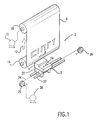
- Figure 1 shows a typical carriage-type ink jet printing device 2.
- a linear array of droplet producing channels is housed in the printhead 4 of the reciprocal carriage assembly 5.
- Ink droplets 6 are propelled to a receiving medium 8 (such as a sheet of paper) that is stepped by a motor 10 a preselected distance in a direction of arrow 12 each time the printhead 4 traverses across the receiving medium 8 in the directions indicated by arrow 14.
- the receiving medium 8 can be stored on a supply roll 16 and stepped onto takeup roll 18 by stepper motor 10 or other means well known to those of skill in the art.
- the printhead 4 is fixedly mounted on the support base 20, which is adapted for reciprocal movement using any well known means, such as two parallel guide rails 22.
- the reciprocal movement of the printhead 4 may be achieved by a cable 24 and a pair of pulleys 26, one of which is powered by a reversible motor 28.
- the printhead 4 is generally moved across the receiving medium 8 perpendicularly to the direction the receiving medium 8 is moved by the motor 10.
- other structures for reciprocating the carriage assembly 5 are possible.
- the linear array of droplet producing channels may extend across the entire width of the receiving medium 8, as is well known to those of skill in the art. This is typically referred to as a full-width array. See, for example, US-A-5,160,403 and US-A-4,463,359.
- Figure 2 shows an ink droplet emitter 30 (or ejector) of one embodiment of a typical ink jet printhead, one of a large plurality of such emitters found in an ink jet printhead. While Figure 2 shows a side-shooter emitter, other emitters such as roof-shooter emitters may similarly be used with the present invention. Typically, such emitters are sized and arranged in linear arrays of 12 to 24 emitters per mm (300 to 600 emitters per inch).
- a silicon member having a plurality of channels for ink droplet emission is known as a "die module" or "chip". Each die module typically comprises 128 emitters, spaced 12 or more to the mm. Generally, a carriage-type printhead will have a single die module.
- An ink jet printhead may have one or more die modules forming a full-width array extending the full width of the receiving medium on which the image is to be printed.
- each die module may include its own ink supply manifold, or multiple die modules may share a common ink supply manifold.
- Each emitter 30 includes a capillary channel 32 terminating in an orifice or nozzle 34.
- the channel 32 holds a quantity of ink 36 maintained within the capillary channel 32 until such time as a droplet of ink is to be emitted.
- Each capillary channel is connected to a supply of ink from an ink supply manifold (not shown).
- the main portion of channel 32 is defined by a groove etched into an upper substrate 38, which is typically made of crystalline silicon.
- the upper substrate 38 abuts a thick-film layer 40, which in turn abuts a lower substrate 42.
- the heating element 46 Sandwiched between the thick film layer 40 and the lower substrate 42 are electrical heating elements 46 for ejecting ink droplets from the capillary channel 32 in a well known manner.
- the heating element 46 is located within a recess 44 formed by an opening in a thick film layer 40.
- the heating element 46 is electrically connected to an addressing electrode 50.
- Each of the ejectors 30 in the printhead 4 has its own heating element 46 and individual addressing electrode 50.
- the addressing electrode 50 is protected by a passivation layer 52.
- Each addressing electrode 50 and heating element 46 is selectively controlled by control circuitry, as will be explained in detail below.
- the heating element 46 when a signal is applied to the addressing electrode 50, the heating element 46 is energized. If the signal is of a sufficient magnitude and/or duration, the heat from the resistive heating element 46 will cause the liquid ink immediately adjacent the heating element 46 to vaporize, creating a bubble 54 of vaporized ink. The force of the expanding bubble 54 ejects an ink droplet 56 (which may include a main droplet and smaller satellite drops) from the orifice 34 onto the surface of the receiving medium 8.
- a plurality of pulses may be applied to the heating element 46 for each ink droplet 56.
- one or more precursor pulses warming pulses
- a print pulse drive pulse
- the print pulse causes the droplet of ink to be ejected.
- the precursor pulses are typically used to raise the temperature of the ink adjacent the heating element and additionally may be used to control the volume of ink to be ejected in each droplet.
- the precursor pulses do not contain enough energy to cause a droplet to be emitted.
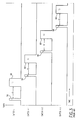
- Figure 3 is a prior art timing diagram showing how a precursor pulse and a print pulse are applied to emitters (or emitter banks) according to a conventional thermal ink jet printhead.
- a precursor pulse 58, having a duration T1 is applied to an emitter i (or emitter bank i) to warm the ink and/or to control a size of the droplet to be ejected. This is followed by a relaxation time of duration T2.
- print pulse 60 of duration T3 is applied to the emitter i.
- another precursor pulse 58 followed by a relaxation time and a print pulse 60 are applied to emitter i+1 (or emitter bank i+1). This process continues across a printhead in serial fashion until all the emitters (or emitter banks) required to eject drops of ink have been addressed.
- Figure 4 is a prior art timing diagram similar to Figure 3 except that in Figure 4 multiple precursor pulses 58 are applied to each emitter 30 prior to the print pulse 60.
- the multiple precursor pulses 58 are shown having durations T4 and T6, respectively and are separated from each other by a relaxation time of duration T5.
- the print pulse 60 is shown having a duration T8 and is separated from the second precursor pulse by a relaxation time of duration T7.
- the durations of all the pulses and relaxation times may vary as required. Similar to the timing diagram shown in Figure 3, the pulses are applied sequentially to a single emitter 30 (or emitter bank) and then are subsequently sequentially applied to the other emitters 30 (or emitter banks) as required to eject the necessary droplets of ink.
- conventional ink jet printheads that use multiple pulses to eject each drop of ink have a printing speed that is limited by the time required to sequentially apply the precursor pulses and print pulses as well as the relaxation times to individual emitters (or emitter banks) of the printhead.
- pulses supplied to at least a first one of a plurality of emitters (or emitter banks) can be interleaved in time with a plurality of power pulses supplied to at least a second one of the emitters (or emitter banks).
- the printing speed of the thermal ink jet printhead is increased with respect to conventional thermal ink jet printheads, as is disclosed in EP 0630751A and as will be further described below.
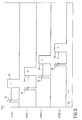
- a precursor pulse 62 having a duration T1 is supplied to a first emitter (or first emitter bank). Then, a relaxation time of duration T2 occurs when no pulses are supplied to the first emitter. Then, a print pulse 64 of duration T3 is applied to the first emitter (or first emitter bank), to cause a drop to be ejected.
- a precursor pulse 62 is applied to a second emitter (or second emitter bank).
- the precursor pulse supplied to later emitters (or emitter banks) are interleaved in time between the precursor pulse and print pulse of previous emitters (or previous emitter banks). In this way, the total time necessary for printing across an entire printhead is reduced.
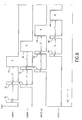
- Figure 6 is a timing diagram illustrating how pulses are interleaved in time according to a preferred embodiment of the present invention.
- Figure 6 is similar to Figure 5, except that in Figure 6, two precursor pulses are applied to each of the emitters (or emitter banks). For any given emitter (or emitter bank), during the relaxation time between the precursor pulses and the print pulse, the precursor pulses of subsequent emitters (or emitter banks) are interleaved. Thus, a second precursor pulse of a second emitter and a first precursor pulse of a third emitter may be interleaved in time between a second precursor pulse and a print pulse of a first emitter.
- a second precursor pulse of a third emitter and a first precursor pulse of the fourth emitter are interleaved in time between a print pulse of a first emitter and a print pulse of a second emitter. Because the pulses are interleaved in time, there is never more than one pulse applied to any of the emitters at a given time.
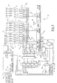
- FIG. 7 is a systems diagram illustrating an embodiment of the present invention having a thermal ink jet printhead 68, a power supply source 66 and a system controller 67.
- the thermal ink jet printhead 68 is activated by two pulses which are interleaved in time and supplied to different emitter banks 96. One of the pulses is controlled by the corresponding data which is to be recorded. In the embodiment shown in Figure 7, there are 128 emitters, organized into 32 emitter banks 96 of four emitters per bank.
- the electrothermal transducers 46 which cause the ink emission are electrically attached to a power supply source 66 via the burn voltage line 70. Each electrothermal transducer 46 is also attached to a power transistor 51 which switches the burn voltage 70 to ground through the transducer 46.
- the emitters are grouped into emitter banks 96 in order to achieve a good balance between the instantaneous power requirements, the number of external electrical leads which must be attached to the printhead, and the time required to provide power pulses to all of the emitters.
- the bank organization creates a set of emitters which can be pulsed individually without exceeding the capacity of the power supply source 66 and power carrying lead 70.
- the bank organization allows the data to be presented to the printhead in units of the number of emitters in a bank 96, four in the embodiment of Figure 7, saving interconnection leads. Also since the several emitters of a bank 96 are able to be pulsed simultaneously, the time required to cycle through all of the emitters of the printhead is reduced to the time needed to cycle through the banks 96.
- a predriver circuit 74 provides the necessary gate voltage level to the power transistor 51 so that it will turn fully on.
- the predriver circuit 74 functions like a logical AND gate having logical inputs from a data line 94 and the emitter bank selection shift register 90.
- the burn voltage and the gate voltage applied to power transistor 51 may be higher than a normal logic level of 3 to 5 volts. Typically the burn voltage is 35 volts to 45 volts and the gate voltage output of the predriver 74 is 7 volts to 14 volts.
- the predriver circuit 74 also serves as the interface between the low voltage logic circuitry and the higher voltage circuitry needed to apply power pulses to the electrothermal transducers 46. The remainder of the circuitry shown in Figure 7 is operated at a typical logic level of 3 to 5 volts.
- a system controller 67 accepts from an image source (not shown) on line 160, a system user interface (not shown) on line 162, such as a user panel or soft display interface, and one or more auxiliary control factor sources (not shown) on line 164, for example a temperature sensing and control system or an input media monitoring system as well as other signals for managing the total operation of the liquid recording apparatus (not shown).
- the overall system controller 67 provides the remaining circuitry with signals conveying data on line 71, direction of printing, also on line 71, data bit shift clocking on line 77, drop emission timing (ENABLE signals) on line 73, and logic circuit reset on line 75.
- the system controller 67 also manages the burn voltage power supply 66 on line 79.
- the data is entered via a DATA/DIRECTION LINE 71 in four bit serial fashion where it is latched by 4-bit serial data latch 82.
- the four bits of data are transferred and latched to the 4-bit parallel data latch 80.
- the LCLK signal as well as the other timing signals PHASE A, PHASE B, SCLK N, and SCLK P are generated by the timing generator circuit 86.
- the function of the timing generator circuit 86 is described in detail below.
- the data is further controlled by a set of four logical AND gates 78, which all have an additional logical input, the PHASE B signal. Therefore, only if the PHASE B signal is high will the four bits of data be presented to the inputs of four logical OR gates 76 and subsequently appear on the four data lines 94.
- a signal PHASE A as an output from timing generator circuit 86, which can also be presented to all of the logical OR gates 76.
- This PHASE A signal is not controlled by the data, but, if presented to the logical OR gates 76, will be passed out to all of the data lines 94. Therefore, the predrivers 74 receive logical inputs from the data lines 94 for either the case of PHASE B AND DATA being high (logically true) or PHASE A being high (logically true).
- the predrivers 74 can thus receive two power pulse commands, one which is the same for every emitter of the emitter bank 96 and derives from PHASE A, and a second which is controlled in time by PHASE B but is given only for emitters which also have DATA logic highs.
- the phase A power pulses are precursor pulses that change the temperature of the ink near the heating element 46, thereby affecting the amount of ink emitted when an emitter receives a subsequent phase B AND DATA power pulse.
- the system controller 67 can modify the duration of the phase A power pulses via the enable signal. This may be accomplished by sensing the temperature of the ink near the emitter, or by sensing the temperature of the printhead near the emitter, with a temperature sensing element, such as in EP-A-0 674 994.
- a temperature sensing element such as in EP-A-0 674 994.
- There are many potential applications of the phase A precursor pulse It can be used in conjunction with a temperature management system to adjust for different printhead and environmental temperature conditions so as to maintain constant ink emission.
- precursor pulses are determined by the overall printer system controller 67. Embodiments of the present invention enable such precursor pulses to be applied to emitters with improved time efficiency, resulting in faster recording speed than conventional devices.
- Power pulsing of individual transducers 46 within an emitter bank 96 is controlled via an input to the predrivers 74 which are connected to the four data lines 94.
- a second input to the predrivers 74 is shared by all of the predrivers 74 of an emitter bank 96.
- These second predriver input lines 92 are controlled by the bank selection shift register 90.
- the bank selection shift register 90 has 32 outputs, F1 - F32, one for each emitter bank 96.
- the corresponding emmiter bank 96 When one of the output lines F1 - F32 is logically high, the corresponding emmiter bank 96 is able to be pulsed since the predrivers 74 of the corresponding bank are now able to close the corresponding power transistor switches 51 in response to signals from the data lines 94.
- the bank selection shift register 90 functions to allow only one emitter bank 96 to be pulsed during any instant of time since the power source has been sized to accommodate only one emitter bank 96 at a time, to synchronize the selection of an emitter bank 96 with the proper set of 4 bits of data appearing on the data lines 94 for that bank 96, and to cycle through all of the emitter banks 96 so that there is an opportunity for every emitter to be activated by both PHASE B pulses and PHASE A pulses.
- the bank selection shift register 90 further provides for the interleaving of the pulses between the emitter banks 96, as illustrated in Figure 5, so that full cycling through all of the banks 96 for the two pulses can be accomplished much more rapidly than if the pulses were not interleaved, as in the prior art illustrated in Figure 3.
- the bank selection shift register 90 is also bi-directional so that the selection of emitter banks 96 can proceed from the first bank to the last bank or vice versa. This is useful for printing as illustrated in Figure 1, whereby the printhead 4 is allowed to print when traversing in both right to left and left to right directions of the carriage 20. Further details about the design of the bank selection shift register 90 are given below in the discussion of Figures 9, 10 and 11.
- the timing generator circuit 86 provides the signals: LCLK, PHASE A, PHASE B, SCLK N, and SCLK P.
- the LCLK causes the 4-bit parallel shift register 80 to latch whatever data is held by the 4-bit serial shift register 82.
- the PHASE A signal allows all of the emitters of an emitter bank 96 to receive power if the bank's bank selection line (F1 - F32) is currently held high by the bank selection shift register 90.
- the PHASE B signal allows each of the emitters of a bank of emitters 96 to receive power if the data line 94 for the emitter is high and the bank's bank selection line (F1 - F32) is being held high by the bank selection shift register 90.
- Shift clock signals SCLK N and SCLK P are non-overlapping logical inverses of each other and cause the bank selection shift register to advance a token bit thereby shifting the selected bank of emitters 96 along the 32-bank row.
- the bank selection shift register 90 operates bi-directionally so that the banks of emitters 96 can be selected in opposite order for printing in bi-directional carriage printer fashion, as illustrated in Figure 1.
- the timing generator circuit 86 derives its output signals from the logic input on the ENABLE LINE 73 and the non-overlapping logical inverse of the signal input on ENABLE LINE 73, both are provided by the non-overlapping signal generator 84, and from the signal input on the FUNCTION CLEAR LINE 75, which serves to logically reinitialize the timing generator circuit 86 at the beginning of each printing cycle. Both the ENABLE and the FUNCTION CLEAR signals are provided by an overall printer system controller 67.
- the timing generator 86 is a signal passing circuit which constructs the output signals from specific logic level transitions present in the ENABLE input signal. The function of the timing generator circuit can be further understood by reference to Figure 8, a timing diagram of the signals which have been described above.
- Figure 8 shows the timing relationships among the following signals: FUNCTION CLEAR (FCLR), ENABLE, PHASE A, PHASE B, F1, F2, F3, F4, SHIFT CLOCK (SCLK N and SCLK P), and LOAD CLOCK (LCLK).
- Figure 8 illustrates the timing relationships for the case of sequentially selecting emitter banks 96 from BANK 1 to BANK 32. Bank selection signals are shown for BANKS 1 - 4 only. Signals for BANKS 5 - 32 would be generated in a continuing sequence in like manner to the signals F1 - F4 before a new FCLR logic transition was sent by the printer system controller. The falling logic level edge 120 of the FCLR signal initializes the circuitry shown in Figure 7.
- the ENABLE signal has a repeating sequence of four logic transition edges: 122, 124, 126, and 128.
- ENABLE logic rising edge 122 is passed by the timing generator circuit 86 to its PHASE A output causing the Phase A rising logic edge 130 and to its LCLK output causing the LCLK rising logic edge 132.
- the rising edge 132 of LCLK latches whatever DATA is appearing at the output of serial data latch 82 into parallel data latch 80.
- the first instance of the rising edge of PHASE A 130 results in power being applied to all of the jet transducers 46 of jet BANK 1 since F1 is also logically high.
- the first logic falling edge 124 of the ENABLE signal is passed by the timing generator 86 to its PHASE A output.
- the PHASE A signal is thereby sent low as indicated by the PHASE A falling edge 134.
- the logical inverse of this first logic falling edge 124 of ENABLE is also available from the non-overlapping signal generator 84 and is passed by the timing generator circuit 86 to its SCLK P output where it causes the SCLK P rising logic edge 136.
- the SCLK P rising logic edge 136 is important to the interleaving function of the Figure 7 circuitry of this preferred embodiment of the invention.
- the logical inverse shift clock, SCLK N is also provided by the timing generator 86 and is also used internally in the bank selection shift register 90 to advance a logical high bit along the cells of the shift register.
- the bank selection signals F1 - F4 will be further explained below in conjunction with the more detailed explanation of the bank selection shift register 90 using the additional Figures 9 - 11.
- the second logic rising edge 126 of the ENABLE signal is passed by the timing generator circuit 86 to its PHASE B output, causing the rising logic edge 138 in the PHASE B signal.
- the PHASE B signal is logically ANDED with the DATA present in the parallel data latch 80 and therefore determines when DATA will be presented to the OR gates 76 for presentation to the data lines 94.
- the second logic falling edge 128 of the ENABLE signal is passed by the timing generator 86 to its PHASE B output, shutting off the presentation of DATA to the OR gates 76, to its SCLK P output and to its LCLK output.
- the logic falling edge 140 allows new DATA to be presented to the parallel data latch 80.
- the ENABLE signal continues to repeat the same sequence of rising and failing logic transitions 122 - 128 causing the events of data latching, PHASE A power pulse firing, PHASE B AND DATA power pulse firing, and sequencing through the banks of emitters 96 until all 32 banks of emitters have been selected for one PHASE A and one PHASE B time period.
- the bank selection shift register 90 described below further functions to interleave the two pulses to a bank of emitters with the pulses to the adjacent banks of emitters, thereby allowing the pulsing of all of the 128 emitters to proceed in a rapid, time efficient fashion.
- the non-overlapping signal generator 85 controls the operation of the 4-bit serial data latch 82.
- a BIT SHIFT signal via line 77 is provided by the overall printer system which is passed by the non-overlapping signal generator 85 to the 4-bit serial data latch 82 in non-overlapping original and logically inverted forms.
- the overall printer system can then present DATA to the DATA/DIRECTION line 71 and clock this DATA into the 4-bit serial data latch 82 at a clock rate determined by the BIT SHIFT line 77. This can be done any time when the LCLK signal output of the timing generator circuit 86 is high without affecting the rest of the data path circuitry elements 80, 78 and 76.
- a direction signal generator 88 which provides to the bank selection shift register 90 the signals DIR N and DIR P.
- the direction signal generator 88 derives from the DATA/DIRECTION line 71 and FUNCTION CLEAR line 75 signals provided by the overall printer system controller 67. This signal establishes whether the bank selection shift register 90 will advance from emitter BANK 1 to emitter BANK 32 (DIR N, high; DIR P, low) or in the opposite direction from emitter BANK 32 to emitter BANK 1 (DIR N, low; DIR P, high).
- the DIR N/P state is set by the logical state of the DATA/DIRECTION line 71 at the time the FCLR makes its rising logic transition 121 shown on the timing diagram of Figure 8.
- the printer system controller 67 Until the next FCLR signal is sent by the printer system controller 67, the DATA/DIRECTION line 71 is used to shift in DATA as described above and the direction signal generator ignores the data signals on this shared line.
- the printer system controller 67 provides the proper direction signal at each FCLR rising logic transition 121.
- a non-overlapping signal generator 87 accepts the FUNCTION CLEAR signal from the printer system controller 67 and generates non-overlapping logical inverses of FUNCTION CLEAR (FCLR and FCLR BUS).
- FCLR BUS the inverse of FCLR, is used internally by the bank selection shift register 90 to initialize internal states of the cells of the shift register 90. This will be explained further below.
- bank selection shift register 90 Such registers are well known in the art. In the simplest form they consist of internal logic cells which can pass and hold a logic state from one cell to the next. Shift registers which are used to transfer logic control along a succession of outputs are also well known as token bit shift registers. The cells of the shift register are all set to logic level 0 (low) and then a single logical value of 1 (high), called the token, is shifted from cell to cell causing the outputs of the cells of the shift register to output the logical 1 (high) moving with each shifting clock event from output to output along the shift register.
- the bank selection shift register 90 is a simple token bit shift register with two additional functions.
- the bank selection shift register 90 also passes the token bit forward one cell for part of the ENABLE signal as generated by the timing generator 86 outputs SCLK N and SCLK P.
- FIG 9 shows the internal organization of the bank selection shift register 90 of Figure 7 in more detail.
- Each of the bank cells 100 has four inputs and four outputs which link adjacent cells to one another and are internal to the bank selection shift register 90.
- Each of the bank cells 100 also has five signal inputs which come from the printer system controller 67 via the FCLR generator 87 (FCLR BUS), via the direction signal generator 88 in Figure 7 (DIR N, DIR P) and via the timing generator 86 in Figure 7 (SCLK N, SCLK P).
- the bank cells 100 each have an output line FN (F1 - F32), which is directly connected to the predrivers 74 of the corresponding emitter banks 96.
- the predrivers 74 of the corresponding emitter bank 96 then close the power transistor switches 51 of that emitter bank 96 if either PHASE A or DATA AND PHASE B high signals are presented by OR gates 76 to the data lines 94.
- the four internal input and four output lines shown for each of the cells 100 of Figure 9 arise because, firstly, for simplicity of design and understanding when constructing shift registers of many cells, it is helpful to designate lines which pass signals from one cell to the next as having both an output end and an input end even though once actually assembled they will be the same wire or conductor run inside the circuit.
- the bank selection shift register 90 is bi-directional, there are two sets of inputs and outputs, one for the "forward" direction (DIR N, high; DIR P, low) and one for the "reverse” direction (DIR N, low; DIR P, high).
- each bank cell 100 the eight internal input and output signal lines shown in Figure 9 for each bank cell 100 are labeled in the following fashion.
- the suffix IN or OUT indicates whether the signal is being used as an input (IN) to the particular bank cell 100 or passed out (OUT) of the particular bank cell 100.
- the three letter root (FWD) or (REV) designates whether that line is active for the forward (FWD) direction of shift register operation (DIR N, high; DIR P, low) or for the reverse (REV) direction of shift register operation (DIR N, low; DIR P, high).
- PP prefix
- the main token signal lines (FWDIN, FWDOUT, REVIN, REVOUT) control the bank selection for receiving power during the PHASE B AND DATA signal period which results in emitters actually emitting print drops of ink.
- the power received by an emitter bank 96 during the PHASE A period is generally intended to precondition the ink temperature thereby affecting the volume and velocity of the ink which will be emitted for emitters subsequently receiving power during the bank's PHASE B period.
- the two end cells 98 shown in Figure 9 supply the initial tokens for both the main token and the prepulse token inputs to either the BANK 1 cell 100 or to BANK 32 cell 100 depending on the direction of operation being determined by the DIR N and DIR P signal lines.
- the DIR N/P lines are set to operate the bank selection shift register 90 from BANK 1 to BANK 32. In this case end register 98 connected to the BANK 1 cell 100 is active.
- the end register 98 In response to the rising logic high edge of the FCLR BUS (the inverse of the falling logic edge 120 shown for the FCLR signal in Figure 8) the end register 98 will provide a pretoken signal on its PPFWDOUT line to the PPFWDIN line of the BANK 1 shift register cell 100.
- This PPFWDOUT signal is passed by the BANK 1 cell 100 to its output F1 as a logic high, shown in the timing diagram Figure 8 as high level 142 on the F1 line.
- the end cell 98 will also provide on its signal line FWDOUT the first main token to the BANK 1 cell 100 on its input line FWDIN.
- the end cell 98 derives this initial main token from the FCLR BUS signal.
- the initial token is latched by the rising logic edge of SCLK P which in turn has been generated by the timing generator circuit 86 from the first falling logic low edge 124 of the ENABLE signal.
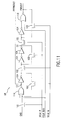
- FIG. 10 the circuit diagram of a bank cell 100 illustrates the eight internal signal lines, the five external signal inputs and the one external output, FN (F1 - F32) together with the pass transistors 102, inverters 104, and logic function circuits 106 - 112 needed create the signals described above.
- FN F1 - F32
- the direction of operation of the shift register can be ignored by considering the operation for one direction since the operation in the opposite direction is the same except that the physical location of the input and output lines changes. Only one set of lines, either FWD lines or REV lines is physically active at any time.
- the forward direction has been selected and so the FWD lines of the cell 100 in Figure 10 are being used.
- the two signal pass transistors 102 controlled by DIR N are therefore on, allowing signal to pass into the cell from the FWDIN and PPFWDIN lines.
- the two signal pass transistors 102 controlled by DIR P are off, stopping signals from passing into the cell from the REVIN and PPREVIN lines.
- the SCLK N and SCLK P lines each control two signal pass transistors 102.
- the two signal pass transistors 102 controlled by SCLK N control the entry of signals from FWDIN into the cell 100 at circuit point S1 in Figure 10.
- the main token is sampled and latched when SCLK N has rising logic edges such as SCLK N edge 144 in Figure 8.
- the two signal pass transistors 102 controlled by SCLK P control the presentation of output signals to FWDOUT in Figure 10. Signals appearing at FWDOUT are presented to the next shift register cell 100 via its FWDIN line.
- FWDOUT signals are also presented to the FN line via NAND gate 110 and NAND gate 112. Therefore high signals at FWDOUT both allow power pulsing of the corresponding bank of emitters 96 and provide a high token signal for the next cell on the next cell's FWDIN line.
- the action of the cell 100 when operating in the forward direction is to accept a high signal on its FWDIN line if one is present from the previous cell's FWDOUT line during one logical high period of SCLK N and then to provide a high signal to the cell's FN line and FWDOUT line during the next logical low period of SCLK N.
- the cell passes a logic low level to the next cell's PPFWDIN line resulting in an F(N+1) high at the output of that next cells NAND gate 112.
- the cell output line FWDOUT is held logically low by NOR gate 106 which has the FCLR BUS signal line as one of its inputs. Only the passage of the main token high signal through latch point S1 overrides this low being set by FCLR BUS and NOR gate 106.
- the above explanation of the main cell 100 operation is largely applicable to the end cell 98 diagrammed in Figure 11.
- An end cell 98 is necessary to begin the process described above of main token acceptance, passing the token forward to allow prepulsing, and passing the main token.
- the end cell 98 shown in Figure 11 is similar to the main cell 100 in that its circuit signal point S2 is equivalent in design and behavior to the circuit points S1 discussed above in conjunction with the main bank cell 100 circuit.
- the end cell 98 has an additional earlier stage which features NOR gate 114 with inputs from FCLR BUS and from ground (GND, logic low or 0) controlled by a SCLK P signal pass transistor 102. This first stage of the circuit generates and latches at circuit point S3 a logic low during the FCLR BUS high signal.
- This logic low at S3 persists during the initial SCLK P low time period (see the timing diagram in Figure 8) and is passed forward on the PPFWDOUT line to the BANK1 cell 100. This allows the first bank of emitters 96 to receive power pulses during the first instance of the PHASE A signal. A logic high state is also latched at circuit point S2 by the FCLR BUS signal. Upon the next transition of the SCLK N and P lines (SCLK P going high, SCLK N going low) this logic high is passed to the FWDOUT line of the end cell 100, providing the initial token to the FWDIN line of the BANK 1 cell 100.
- the BANK1 cell 100 is not ready to pass this signal to its F1 NAND gate 112 so no power pulsing occurs for this very first PHASE B period.
- the sequencing of bank selection for PHASE A and PHASE B power pulses then continues in the fashion described above in the explanation of the bank selection main cell 100.
- the timing diagram in Figure 8 shows the interleaved FN signals generated by the bank selection shift register 90 for the first 4 emitter banks 96.
- a second preferred embodiment of the invention is shown in the system diagram of Figure 12.
- the circuit is similar to the embodiment diagrammed in Figure 7. All like elements of this second embodiment are numbered in like manner to the elements of Figure 7. There are three differences in this second embodiment all related to enabling the data to control which emitters are pulsed within an emitter bank 96 during PHASE A, in like manner to the previous embodiment, wherein the data controlled the individual emitter pulsing during PHASE B.
- This new function of allowing PHASE A power pulses only for emitters with corresponding data values of logical 1 (true) is accomplished by expanding the input serial data latch to the 8-bit latch 83, adding a second 4-bit parallel data latch 80 and adding four additional AND gates 78.
- the AND gates 78 perform the logical operation of ANDING the data presented by the lower 4-bit parallel data latch 80 with the PHASE A signal from the timing generator circuit 86.
- the outputs of the four lower AND gates are connected to the OR gates 76.
- 4 bits of DATA are shifted into the lower four cells of 8-bit serial register 83. These bits are loaded into the lower 4-bit parallel data latch 80. They are ANDED with the PHASE A signal so that only signals which are logically DATA AND PHASE A will be presented to the OR gates 76 for presentation to the data lines 94.
- a next set of 4 bits of DATA is then shifted into 8-bit serial register 83, moving the previous 4 bits of DATA into the upper half of latch 83.
- the pulse interleaving circuitry operates exactly the same for this second embodiment as described above for the embodiment diagrammed in Figure 7.
- the embodiment of Figure 12 can also be extended to the case of three or more activation pulses by adding a set of serial and parallel data latches and AND gates for each activation pulse PHASE.
- a third embodiment of the invention can be envisioned in which the ENABLE signal logical transition edges are changed by the printer system controller 67 and/or the power applied via the BURN VOLTAGE lines in Figures 7 and 12 is changed by the overall printer system controller 67 and the power supply source 66 to further modulate the power being applied to the liquid emitters.
- the function of interleaving the pulses in time and controlling some or all of the pulses by the data can be carried out in like fashion to the embodiments described above.
Landscapes
- Particle Formation And Scattering Control In Inkjet Printers (AREA)
- Ink Jet (AREA)
- Control Or Security For Electrophotography (AREA)
- Handling Of Sheets (AREA)
Claims (9)
- Un appareil à enregistrement à liquide pour former une image sur un support d'enregistrement (8) en fonction de données d'image, comprenant :une source d'énergie (66) fournissant des impulsions de puissance, chaque impulsion de puissance comprenant des impulsions-précurseurs (62) et une impulsion d'impression (64) ;une tête d'enregistrement (4) comportant une pluralité de distributeurs de liquide (30) dont chacun émet sélectivement une goutte de liquide sur le support d'enregistrement en réponse à l'une des impulsions d'impression, chaque impulsion d'impression étant précédée d'une des impulsions-précurseurs ; etun dispositif de commande (67) qui connecte sélectivement (51) chacun de la pluralité de distributeurs de liquide à la source d'énergie afin de délivrer la pluralité d'impulsions de puissance aux distributeurs de liquide, caractérisé en ce que les impulsions d'impression (64) sont alimentées à des distributeurs adjacents de sorte qu'au moins deux impulsions-précurseurs fournies à une pluralité de distributeurs successifs soient entrelacées dans le temps entre les impulsions d'impression des distributeurs adjacents.
- Un appareil selon la revendication 1, dans lequel les impulsions de puissance (62, 64) sont générées en fonction des données d'image.
- Un appareil selon la revendication 1 ou 2, dans lequel les distributeurs de liquide (30) comprennent chacun un élément de dispositif de chauffage (46) et les impulsions-précurseurs (62) forcent l'élément de dispositif de chauffage à chauffer le liquide adjacent à l'élément de dispositif de chauffage sans émettre une goutte du liquide.
- Un appareil selon l'une des revendications 1 à 3, dans lequel les distributeurs de liquide sont groupés en batteries (96) dont chacune comprend une pluralité de distributeurs de liquide, et les plusieurs impulsions de puissance alimentées aux distributeurs de liquide à l'intérieur d'au moins une première des batteries de distributeurs de liquide sont entrelacées dans le temps avec la pluralité d'impulsions de puissance fournies aux distributeurs de liquide à l'intérieur d'au moins une deuxième des batteries de distributeurs de liquide.
- Un appareil à enregistrement à liquide selon l'une quelconque des revendications 1 à 3, dans lequel la tête d'enregistrement comprend une tête d'impression à jet d'encre (4) comportant une pluralité de batteries (96) de distributeurs, chacun des distributeurs étant activé par une pluralité d'impulsions de puissance afin d'émettre une goutte d'encre sur le support d'enregistrement ; et
le dispositif de commande comprend une circuiterie de verrouillage de données (82) qui reçoit, verrouille et produit les données d'image, une circuiterie de groupage de batteries (78, 76) connectée à la circuiterie de verrouillage de données qui reçoit les données d'image et dirige les données d'image vers les batteries de distributeurs, et une circuiterie de programmation (67) qui sélectionne, à un instant quelconque, au maximum une seule des batteries (96) de distributeurs et force des impulsions-précurseurs fournies à une pluralité de batteries d'émetteurs successives à être entrelacées dans le temps entre les impulsions d'impression (64) fournies à des batteries d'émetteurs adjacentes. - Un appareil selon la revendication 5, comprenant en outre une circuiterie de synchronisation (86) qui génère dessignaux de synchronisation et des signaux d'horloge de programmation de puissance, les signaux de synchronisation définissant un temps de cycle de tête d'impression et les signaux d'horloge de programmation de puissance ayant une pluralité de phases, dans lequel les signaux de synchronisation sont acheminés à la circuiterie de verrouillage de données tandis que les signaux d'horloge de programmation de puissance sont acheminés à la circuiterie de programmation.
- Un appareil selon la revendication 5 ou 6, dans lequel chacune des impulsions d'impression fait qu'au moins une goutte d'encre est émise des distributeurs à l'intérieur de la batterie d'émetteurs correspondante.
- Un appareil selon l'une quelconque des revendications précédentes, comprenant en outre un moyen permettant de faire varier la durée des impulsions de puissance en fonction d'au moins un facteur autre que les données d'image.
- Une méthode pour former une image sur un support d'enregistrement (8) en fonction de données d'image, comprenant les étapes consistant à :caractérisée par l'étape consistant à diriger sélectivement (67, 51) les impulsions vers les distributeurs de liquide de sorte qu'au moins deux impulsions-précurseurs (62) fournies à une pluralité de distributeurs de liquide successifs soient entrelacées dans le temps entre les impulsions d'impression (64) fournies à des distributeurs adjacents.fournir une pluralité d'impulsions de puissance, chaque impulsion comprenant des impulsions-précurseurs (62) et une impulsion d'impression (64) ; etdiriger sélectivement la pluralité d'impulsions vers au moins une pluralité de distributeurs de liquide (30) placés sur une tête d'enregistrement (4), les distributeurs de liquide émettant chacun une goutte de liquide en réponse à une pluralité d'impulsions ;
Applications Claiming Priority (2)
| Application Number | Priority Date | Filing Date | Title |
|---|---|---|---|
| US40110995A | 1995-03-08 | 1995-03-08 | |
| US401109 | 1995-03-08 |
Publications (3)
| Publication Number | Publication Date |
|---|---|
| EP0730962A2 EP0730962A2 (fr) | 1996-09-11 |
| EP0730962A3 EP0730962A3 (fr) | 1997-07-09 |
| EP0730962B1 true EP0730962B1 (fr) | 2004-06-09 |
Family
ID=23586342
Family Applications (1)
| Application Number | Title | Priority Date | Filing Date |
|---|---|---|---|
| EP96301565A Expired - Lifetime EP0730962B1 (fr) | 1995-03-08 | 1996-03-07 | Méthode et appareil pour entrelacer des impulsions dans un dispositif d'enregistrement à liquide |
Country Status (6)
| Country | Link |
|---|---|
| US (1) | US5917509A (fr) |
| EP (1) | EP0730962B1 (fr) |
| JP (1) | JPH08258267A (fr) |
| BR (1) | BR9600953A (fr) |
| CA (1) | CA2168994C (fr) |
| DE (1) | DE69632657T2 (fr) |
Families Citing this family (28)
| Publication number | Priority date | Publication date | Assignee | Title |
|---|---|---|---|---|
| JP3337912B2 (ja) * | 1996-06-28 | 2002-10-28 | キヤノン株式会社 | インクジェットヘッドの駆動方法及びこれを実行するインクジェット装置 |
| US5971518A (en) * | 1997-01-28 | 1999-10-26 | Lexmark International, Inc. | Method of printing with an ink jet printer to inhibit the formation of a print artifact |
| JP3637468B2 (ja) * | 1997-01-30 | 2005-04-13 | コニカミノルタホールディングス株式会社 | プリンタの駆動装置及びプリンタ |
| US6322187B1 (en) | 2000-01-19 | 2001-11-27 | Xerox Corporation | Method for smoothing appearance of an ink jet print |
| US6361153B1 (en) | 2000-02-17 | 2002-03-26 | Xerox Corporation | Preload of data prior to fire pulse by using a dual buffer system in ink jet printing |
| US6523923B2 (en) * | 2000-10-16 | 2003-02-25 | Brother Kogyo Kabushiki Kaisha | Wavefrom prevents ink droplets from coalescing |
| JP4666810B2 (ja) | 2001-05-24 | 2011-04-06 | キヤノン株式会社 | 画像記録装置およびその制御方法 |
| US6585343B2 (en) * | 2001-10-31 | 2003-07-01 | Hewlett-Packard Development Company, L.P. | System and method for using pulse or trickle warming to control neutral color balance on a print media |
| KR100441607B1 (ko) * | 2002-10-22 | 2004-07-23 | 삼성전자주식회사 | 프린터 헤드의 직렬 데이타 어드레스 전송 방법 및 장치 |
| US6698862B1 (en) * | 2003-01-16 | 2004-03-02 | Xerox Corporation | Method and apparatus for thermal ink jet drop volume control using variable prepulses |
| WO2005102720A1 (fr) * | 2004-03-23 | 2005-11-03 | Lexmark International, Inc | Procede et appareil de declenchement des buses d'une imprimante a jet d'encre |
| US7497536B2 (en) * | 2004-04-19 | 2009-03-03 | Hewlett-Packard Development Company, L.P. | Fluid ejection device |
| KR100654765B1 (ko) * | 2005-09-26 | 2006-12-08 | 삼성전자주식회사 | 헤드구동장치와 이를 포함하는 잉크젯 프린터 및 그데이터처리방법 |
| JP5081019B2 (ja) * | 2007-04-02 | 2012-11-21 | キヤノン株式会社 | 記録ヘッド用の素子基板、記録ヘッド、ヘッドカートリッジ、及び記録装置 |
| JP5106173B2 (ja) * | 2008-02-22 | 2012-12-26 | 理想科学工業株式会社 | 印刷装置および印刷処理方法 |
| JP5334271B2 (ja) * | 2011-06-03 | 2013-11-06 | 富士フイルム株式会社 | 液体吐出ヘッドの駆動装置、液体吐出装置及びインクジェット記録装置 |
| JP6083979B2 (ja) * | 2012-08-31 | 2017-02-22 | キヤノン株式会社 | 記録ヘッド |
| US9862187B1 (en) | 2016-08-22 | 2018-01-09 | RF Printing Technologies LLC | Inkjet printhead temperature sensing at multiple locations |
| US9981465B1 (en) | 2017-02-20 | 2018-05-29 | RF Printing Technologies LLC | Inkjet printing apparatus with firing or heating waveform selector |
| PL4206896T3 (pl) | 2019-02-06 | 2024-10-28 | Hewlett-Packard Development Company L.P. | Identyfikacja bitów losowych w pakietach danych sterujących |
| EP3717254B1 (fr) | 2019-02-06 | 2023-12-20 | Hewlett-Packard Development Company, L.P. | Circuit intégré à circuits d'attaque d'adresse pour puce fluidique |
| WO2020162894A1 (fr) | 2019-02-06 | 2020-08-13 | Hewlett-Packard Development Company, L.P. | Paquets de données comprenant des nombres aléatoires pour commander des dispositifs de distribution de fluide |
| MX2021008897A (es) | 2019-02-06 | 2021-08-19 | Hewlett Packard Development Co | Componente de impresion con circuito de memoria. |
| US11787173B2 (en) | 2019-02-06 | 2023-10-17 | Hewlett-Packard Development Company, L.P. | Print component with memory circuit |
| AU2019428636B2 (en) * | 2019-02-06 | 2023-11-16 | Hewlett-Packard Development Company, L.P. | Memories of fluidic dies |
| DK3717246T3 (da) | 2019-02-06 | 2021-07-19 | Hewlett Packard Development Co | Flere kredsløb koblet til en grænseflade |
| CN115723430A (zh) | 2019-02-06 | 2023-03-03 | 惠普发展公司,有限责任合伙企业 | 打印部件和操作打印部件的方法 |
| SG11202107300YA (en) | 2019-02-06 | 2021-08-30 | Hewlett Packard Development Co Lp | Communicating print component |
Family Cites Families (9)
| Publication number | Priority date | Publication date | Assignee | Title |
|---|---|---|---|---|
| US4774530A (en) * | 1987-11-02 | 1988-09-27 | Xerox Corporation | Ink jet printhead |
| US4982199A (en) * | 1988-12-16 | 1991-01-01 | Hewlett-Packard Company | Method and apparatus for gray scale printing with a thermal ink jet pen |
| US5172134A (en) * | 1989-03-31 | 1992-12-15 | Canon Kabushiki Kaisha | Ink jet recording head, driving method for same and ink jet recording apparatus |
| US5138337A (en) * | 1990-05-10 | 1992-08-11 | Eastman Kodak Company | Apparatus for grey level printing using a binary architectured printhead |
| US5265315A (en) * | 1990-11-20 | 1993-11-30 | Spectra, Inc. | Method of making a thin-film transducer ink jet head |
| ATE237474T1 (de) * | 1991-01-18 | 2003-05-15 | Canon Kk | Tintenstrahlaufzeichnungsverfahren und - vorrichtung mit thermischer energie |
| DE69232385T2 (de) * | 1991-03-20 | 2002-07-11 | Canon K.K., Tokio/Tokyo | Temperatursteuerung für thermischen Tintenstrahlaufzeichnungskopf |
| JP3391889B2 (ja) * | 1993-06-23 | 2003-03-31 | キヤノン株式会社 | インクジェット記録方法及び記録装置 |
| JP3581445B2 (ja) * | 1994-08-24 | 2004-10-27 | キヤノン株式会社 | 記録方法およびその装置 |
-
1996
- 1996-02-07 CA CA002168994A patent/CA2168994C/fr not_active Expired - Lifetime
- 1996-02-29 JP JP8042312A patent/JPH08258267A/ja active Pending
- 1996-03-07 DE DE69632657T patent/DE69632657T2/de not_active Expired - Lifetime
- 1996-03-07 EP EP96301565A patent/EP0730962B1/fr not_active Expired - Lifetime
- 1996-03-07 BR BRPI9600953-5A patent/BR9600953A/pt not_active IP Right Cessation
-
1997
- 1997-05-29 US US08/864,893 patent/US5917509A/en not_active Expired - Lifetime
Also Published As
| Publication number | Publication date |
|---|---|
| CA2168994A1 (fr) | 1996-09-09 |
| EP0730962A3 (fr) | 1997-07-09 |
| BR9600953A (pt) | 1997-12-30 |
| DE69632657D1 (de) | 2004-07-15 |
| CA2168994C (fr) | 2000-01-18 |
| JPH08258267A (ja) | 1996-10-08 |
| EP0730962A2 (fr) | 1996-09-11 |
| US5917509A (en) | 1999-06-29 |
| DE69632657T2 (de) | 2005-06-16 |
Similar Documents
| Publication | Publication Date | Title |
|---|---|---|
| EP0730962B1 (fr) | Méthode et appareil pour entrelacer des impulsions dans un dispositif d'enregistrement à liquide | |
| US6540333B2 (en) | Dynamic memory based firing cell for thermal ink jet printhead | |
| EP0551013B1 (fr) | Ensemble de tête d'enregistrement pour appareil d'enregistrement par jet d'encre et sa méthode de commande | |
| US5600349A (en) | Method of reducing drive energy in a high speed thermal ink jet printer | |
| US7815273B2 (en) | Fluid ejection device | |
| US6698862B1 (en) | Method and apparatus for thermal ink jet drop volume control using variable prepulses | |
| KR100871543B1 (ko) | 잉크젯 프린팅 시스템 및 잉크젯 프린트헤드 | |
| US7104624B2 (en) | Fire pulses in a fluid ejection device | |
| KR100871542B1 (ko) | 잉크젯 프린트헤드 및 그 작동 방법 | |
| JP4402880B2 (ja) | インクを噴出させるための方法および装置 | |
| KR20040010207A (ko) | 잉크젯 기록 헤드, 잉크젯 기록 헤드의 구동 방법 및 잉크젯 기록 헤드용 기판 | |
| US6431685B1 (en) | Printing head and printing apparatus | |
| US7090338B2 (en) | Fluid ejection device with fire cells | |
| US6527355B1 (en) | Method and apparatus for preventing banding defects caused by drop mass variations in an ink jet printer | |
| JP3441743B2 (ja) | インクジェット記録装置 | |
| JP2010511530A (ja) | データ信号ラッチ回路を備える流体吐出デバイス | |
| JPH07125261A (ja) | 記録装置及び該装置における記録濃度調整方法 | |
| JPH01290437A (ja) | 液体噴射記録ヘッドの制御装置 |
Legal Events
| Date | Code | Title | Description |
|---|---|---|---|
| PUAI | Public reference made under article 153(3) epc to a published international application that has entered the european phase |
Free format text: ORIGINAL CODE: 0009012 |
|
| AK | Designated contracting states |
Kind code of ref document: A2 Designated state(s): DE FR GB |
|
| PUAL | Search report despatched |
Free format text: ORIGINAL CODE: 0009013 |
|
| AK | Designated contracting states |
Kind code of ref document: A3 Designated state(s): DE FR GB |
|
| 17P | Request for examination filed |
Effective date: 19980109 |
|
| 17Q | First examination report despatched |
Effective date: 20010219 |
|
| GRAP | Despatch of communication of intention to grant a patent |
Free format text: ORIGINAL CODE: EPIDOSNIGR1 |
|
| GRAS | Grant fee paid |
Free format text: ORIGINAL CODE: EPIDOSNIGR3 |
|
| GRAA | (expected) grant |
Free format text: ORIGINAL CODE: 0009210 |
|
| AK | Designated contracting states |
Kind code of ref document: B1 Designated state(s): DE FR GB |
|
| REG | Reference to a national code |
Ref country code: GB Ref legal event code: FG4D |
|
| REF | Corresponds to: |
Ref document number: 69632657 Country of ref document: DE Date of ref document: 20040715 Kind code of ref document: P |
|
| ET | Fr: translation filed | ||
| PLBE | No opposition filed within time limit |
Free format text: ORIGINAL CODE: 0009261 |
|
| STAA | Information on the status of an ep patent application or granted ep patent |
Free format text: STATUS: NO OPPOSITION FILED WITHIN TIME LIMIT |
|
| REG | Reference to a national code |
Ref country code: GB Ref legal event code: 732E |
|
| 26N | No opposition filed |
Effective date: 20050310 |
|
| REG | Reference to a national code |
Ref country code: FR Ref legal event code: TP |
|
| REG | Reference to a national code |
Ref country code: FR Ref legal event code: PLFP Year of fee payment: 20 |
|
| PGFP | Annual fee paid to national office [announced via postgrant information from national office to epo] |
Ref country code: DE Payment date: 20150318 Year of fee payment: 20 |
|
| PGFP | Annual fee paid to national office [announced via postgrant information from national office to epo] |
Ref country code: GB Payment date: 20150225 Year of fee payment: 20 Ref country code: FR Payment date: 20150320 Year of fee payment: 20 |
|
| REG | Reference to a national code |
Ref country code: DE Ref legal event code: R071 Ref document number: 69632657 Country of ref document: DE |
|
| REG | Reference to a national code |
Ref country code: GB Ref legal event code: PE20 Expiry date: 20160306 |
|
| PG25 | Lapsed in a contracting state [announced via postgrant information from national office to epo] |
Ref country code: GB Free format text: LAPSE BECAUSE OF EXPIRATION OF PROTECTION Effective date: 20160306 |
|
| REG | Reference to a national code |
Ref country code: GB Ref legal event code: 732E Free format text: REGISTERED BETWEEN 20170406 AND 20170412 |
|
| REG | Reference to a national code |
Ref country code: FR Ref legal event code: TP Owner name: S-PRINTING SOLUTION CO., LTD., KR Effective date: 20170912 |