EP0731412A1 - Dispositif électronique pour ordinateur - Google Patents
Dispositif électronique pour ordinateur Download PDFInfo
- Publication number
- EP0731412A1 EP0731412A1 EP96301581A EP96301581A EP0731412A1 EP 0731412 A1 EP0731412 A1 EP 0731412A1 EP 96301581 A EP96301581 A EP 96301581A EP 96301581 A EP96301581 A EP 96301581A EP 0731412 A1 EP0731412 A1 EP 0731412A1
- Authority
- EP
- European Patent Office
- Prior art keywords
- memory
- address
- cpu
- bus
- computer device
- Prior art date
- Legal status (The legal status is an assumption and is not a legal conclusion. Google has not performed a legal analysis and makes no representation as to the accuracy of the status listed.)
- Granted
Links
Images





Classifications
-
- G—PHYSICS
- G06—COMPUTING OR CALCULATING; COUNTING
- G06F—ELECTRIC DIGITAL DATA PROCESSING
- G06F15/00—Digital computers in general; Data processing equipment in general
- G06F15/76—Architectures of general purpose stored program computers
- G06F15/78—Architectures of general purpose stored program computers comprising a single central processing unit
- G06F15/7839—Architectures of general purpose stored program computers comprising a single central processing unit with memory
- G06F15/7864—Architectures of general purpose stored program computers comprising a single central processing unit with memory on more than one IC chip
-
- G—PHYSICS
- G06—COMPUTING OR CALCULATING; COUNTING
- G06F—ELECTRIC DIGITAL DATA PROCESSING
- G06F13/00—Interconnection of, or transfer of information or other signals between, memories, input/output devices or central processing units
- G06F13/38—Information transfer, e.g. on bus
- G06F13/40—Bus structure
- G06F13/4063—Device-to-bus coupling
- G06F13/4068—Electrical coupling
Definitions
- the present invention relates to an electronic computer device which activates an alternative CPU in place of a packaged CPU on a mother board of a personal computer and controls the personal computer by the alternative CPU.
- accelerators which afford higher performance to existing personal computers
- electronic devices such as accelerators which afford higher performance to existing personal computers
- accelerators which afford higher performance to existing personal computers
- They activate an alternative CPU in place of a packaged CPU on the mother board.
- Various accelerators have been developed and sold, ranging from the one which simply substitutes the packaged CPU with a high-performance CPU to the one which incorporates e.g. a high-speed clock generating circuit based on the mother-board-side clock or a control circuit exclusively for timing with the mother board side.
- Utilization of these electronic computer devices enables both increase in the functions and speed of the CPU which controls the personal computer and continual use of the peripherals, such as a packaged hard disk, as well as the main memory DRAM on the mother board and the image display VRAM. Therefore, the processing performance of the personal computer is up-graded economically and thus information processing operations can be carried out efficiently since high-level-function software which results in a high load is available.
- Some computers are provided with a virtual memory function which utilizes an empty area of the hard disk as a part of the main memory and the main memory area is thus expanded by such virtual memory.
- Many personal computers are provided with an expansion slot connected to a low-speed bus for mounting of any of the various expansion boards, where a memory board which is mounted with memory chips and inserted in the expansion slot can be used as the main memory.
- a memory board which is mounted with memory chips and inserted in the expansion slot can be used as the main memory.
- operation of software requiring a large capacity of memory is available but the benefit of the alternative CPU which is capable of high-speed operation is not available due to decrease in the memory access speed. This results from extremely low access speed of the hard disk and the memory board connected to the expansion slot.
- a purpose of the electronic computer device is to resolve such issues as above through enhancement of a total processing performance of the personal computers and the high-speed processing of high-level-function software which requires a large memory area and complicated processing.
- an electronic computer device comprises:
- the alternative CPU which is connected to the main memory of the computer and the peripherals via connectors controls the personal computer.
- the memory means which is connected to the expansion memory bus extended from the memory control terminal of the alternative CPU accesses the predetermined address of the memory means which is connected to the expansion memory bus when the memory address pointed by the alternative CPU is in the expanded memory address area.
- Fig. 1 is a plan showing the components side of the electronic computer device 20 as an embodiment of the present invention.
- Fig. 2 is a rear surface plan showing the solder side of the electronic computer device 20.
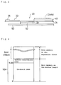
- Fig. 3 is a side view showing the state where the electronic computer device 20 is mounted on the mother board 50.
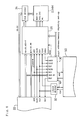
- Fig. 4 shows a memory map of the electronic computer device 20 as an embodiment.
- Fig. 5 is a schematic drawing showing the electric connections between the electronic computer device 20 and the mother board 50.
- Fig. 6 is a block diagram showing an internal configuration of the memory control component MC of the electronic computer device 20.
- Fig. 7 is an illustrative drawing showing the internal configuration of the memory control IC which is a part of the memory control component MC, where the functions are respectively shown in each block.
- Fig. 8 is an illustrative drawing showing the processing at the time of request for DMA transfer to the expansion memory area of the electronic computer device 20.
- Fig. 9 is a flowchart showing the interrupt processing at the time of carrying out DMA transfer.
- FIGs. 1 and 2 are drawings showing the components side (top plan) and the solder surface (rear-surface plan) of an electronic computer device 20 as the embodiment.
- an Intel i486DX4 (a registered trade name of Intel) is mounted as a high-performance alternative CPU 22.
- This electronic computer device 20 is basically designed, as described below, so as to operate in place of a packaged CPU on a mother board 50 when attached to an ODP (over drive processor) socket 52 on the mother board 50 of a personal computer. Therefore, a large number of components are efficiently packaged on an extremely small PCB (Printed Circuit Board) 24 so as to eliminate contact with other packaged components at the time of mounting it on the mother board.
- PCB Print Circuit Board
- Peripheral circuits such as a memory control IC 28, a PLD 30, a clock driver 32 and a power supply IC 36, are arranged on the top of the PCB 24, as in Fig. 1.
- Bus drivers 34, a connector 38 for attachment to the mother board 50, more than one bypass capacitor group 39 for reduction in impedance of the power supply line leading to the alternative CPU 22 and other components are provided on the rear side, as in Fig. 2. Due to drawing limitations, other bypass capacitors and resistors packaged on the surface as a surface-package-type packaging are eliminated in Figs. 1 and 2.
- Two expansion slots 40 for DIMMs are connected to the memory bus of the alternative CPU 22, where two 1-, 4-, 8- 16- or 32-Mbyte DIMMs may be mounted.
- the supply voltage of the alternative CPU 22 of the electronic computer device 20 is different from the supply voltage of the mother board 50 (5V) or, if an energy-saving CPU which operates at 3.3V is adopted, the power supply IC 36 supplies 3.3V stable supply voltage power for the electronic computer device 20 from the power source in the mother board 50. If the energy-saving CPU is adopted, this power supply IC 36 is attached to the PCB 24.
- Fig. 3 is a side view showing the state where the electronic computer device 20 is attached to an ODP socket 52 on the mother board 50 by the connector 38.
- a system which adopts an Intel CPU, i486DX, i486DX2 or i486SX, as a packaged CPU is provided with the socket 52 for mounting of an ODP on the mother board 50.
- a computer which is provided with the ODP socket 52 has a constitution where the alternative CPU starts operation in place of the packaged CPU while the packaged CPU is inactive without removing the packaged CPU from the mother board if the alternative CPU 22 is attached to the socket 52.
- FIG. 3 shows an example of the constitution where the alternative CPU for the electronic computer device 20 is directly inserted into the ODP socket 52 but this is only an example and a variety of other constitutions are available; such as a constitution where it is directly inserted into the socket for the packaged CPU after removal of the packaged CPU on the mother board 50 and a constitution where a socket for a co-processor on the mother board 50 is utilized.
- the address width of the memory bus of the packaged CPU provided on the mother board 50 is 24 bits, a maximum of 16 Mbyte range can be addressed as main memory.
- the higher-order memory area in this range is a system reservation area which is used by the system, such as BIOS stored in a ROM or other device on the mother board 50, which is not shown in the figure, and thus only 14.6 Mbyte range is available for application software and so on.
- the electronic computer device 20 is connected to the address bus on the mother board 50 on attachment to the ODP socket 52.
- the connections are outlined in Fig. 5.
- the electronic computer device 20 as an embodiment roughly consists of the alternative CPU 22 which is capable of high-speed operation, the expansion memory which is provided of the DIMM type and the memory control component MC which performs memory control; and the alternative CPU 22 and the memory control component MC are connected to the address bus, the data bus and other control bus from the mother board 50 via the ODP socket 52.
- Fig. 6 shows a detailed constitution of the memory control component MC to elucidate the connections between the mother board 50 and the alternative CPU 22 as well as the expansion memory.
- the memory control component MC consists of the memory IC 28, the PLD 30, the clock driver 32 and the bus driver 34. The memory control component MC performs control when the alternative CPU 22 accesses the DIMM inserted in the expansion slot 40 on the electronic computer device 20.
- Every bus (address bus, data bus, control bus, and so on) is under the control of the alternative CPU 22 which is connected to the ODP socket 52 on the mother board 50.
- the address bus of the alternative CPU 22 is provided with the width of A0 through A26 which is a sufficient address space for 16 Mbytes on the mother board and 64 Mbytes of two 32-Mbyte DIMMs inserted in the expansion slots 40.
- the memory control component MC is connected to every bus in the same way as the alternative CPU 22 and naturally connects the DIMMs inserted in the expansion slots 40 and each signal line and controls the address strobe signal (hereinafter referred to as ADS) which is output to the mother board 50 and the ready signal (hereinafter referred to as RDY) which is output from the mother board 50.
- ADS address strobe signal
- RDY ready signal
- the PLD 30 also performs arbitration between the RDY signal from the mother board 50 and the RDY signal from the expansion memory on the electronic computer device 20, or simply performs a logical OR operation. Additionally, the PLD 30 outputs the refresh signal (RFSH) to the memory control IC 28 while the hold acknowledge signal (HLDA) is being output from the alternative CPU 22 so as to control the timing of refreshing the DRAM in the expansion slot 40.
- RFSH refresh signal
- HLDA hold acknowledge signal
- the clock signal (CLK) is multiplied by the PLD 30 and the clock driver 32 at the memory control component MC to generate new clock (CLK) signals which are 1.5-, 2- and 3-times multiplications of the CLK signal. Since all the synchronous elements on the side of the mother board operate in synchronism with the CLK, several kinds of rate-multiplied clocks are generated to operate the alternative CPU 22 on the electronic computer device 20 at the allowable maximum operating frequency while maintaining synchronism with those elements. When only the speed of the alternative CPU 22 is increased, the entire operating speed is not much improved if the peripheral elements operate only at low speeds. When the alternative CPU 22 and the clock for all the connected elements are optimized, a maximum operating speed of the electronic computer device 20 itself is attained.
- the rate-multipliers are set up by an external circuit, such as a jumper wire or a dip switch, which is not shown in the figure.
- the memory control IC 28 receives address signals and control signals from the alternative CPU 22 and generates control signals for various DRAMs used in the DIMMs.
- the DRAMs are varied such as in the access mode as well as in the capacity.
- the memory control IC 28 comprises "mode” 28A which is a block where the DRAM operation mode, the start address and so on are set up, "cs-status” 28B which is a decoder where the CPU bus cycle is monitored, "ma” 28C which is a block where the multiplexed address for the DRAM is output, "rasacc” 28D which is a block where the RAS access is controlled, “preras” 28E which is a block where the RAS is precharged, "casacc” 28F which is a block where CAS access is controlled, “ras” 28G which is a block where the RAS pulse is controlled, “cas” 28H which is a block where the CAS pulse is controlled, and "buffer” 28I which is a block where the data bus buffer is controlled.
- mode 28A is a block where various modes are set up. Input of predetermined signals from external circuits to "mode” enables arbitrary setting up of such as whether a wait cycle is required for the memory access or not, whether the output width of the RDY is one clock or the output is held until a response from the outside is gained, the start address of the expansion memory (above 16 Mbytes in this embodiment, as in Fig. 4), and the expansion memory capacity and the access mode matching the DRAM in use.
- "cs-status" 28B is in charge of monitoring and decoding of the CPU bus cycle, which executes the address decoding and the CPU cycle decoding of such as the IO cycle, the code access and the data access.
- "ma” 28C performs the multiplex processing of the RAS address and the CAS address and the RAS address generation processing under the control of "rasacc” 28D.
- "ma” 28C outputs multiplexed address signals MA0 through MA10.
- "rasacc” 28D performs the monitoring of whether the paging is continuous or not, and instruction of the RAS precharge start by the monitoring of completion of refreshing and by the monitoring of completion of DMA.
- "preras” 28E is the block which actually generates the RAS precharge cycle pulse which is synchronous with the memory access on receiving the controlling output from “rasacc” 28D.
- the controlling output of “rasacc” 28D is also input to "casacc” 28F where the CAS timing signal is generated in synchronism with the memory access.
- "Ras” 28G and “cas” 28H are the blocks where the RAS pulses 00N through 20N and the CAS pulses CAS 00N through 30N are generated respectively; selection from the two expansion slots 40 is performed by the RAS pulses and the access is performed by the CAS pulses in the data width (long word, word or byte) as instructed by "cs-status".
- the memory control IC 28 in this embodiment can accept a first-page-mode DRAM which performs a high-speed data access by varying the CAS signals only while maintaining the RAS signal as low-active.
- Buser 28I is the block which controls the directions of the input and output signals of the bus driver 34, which decides on the transfer direction of the data bus information, whether from the expansion slots 40 to the alternative CPU 22 or from the alternative CPU 22 to the expansion slots 40, and which controls the bus driver 34 with its output DIR.
- the alternative CPU 22 of the electronic computer device 20 executes internal processing, such as arithmetic operation, at a high clock frequency appropriate to the alternative CPU 22.
- internal processing such as arithmetic operation
- the memory control component MC while the memory elements packaged on the mother board 50 are utilized as for the main memory addresses in the 16-Mbyte memory area and the DIMMs inserted in the expansion slots 40 are utilized as the main memory to read and write data in the higher-order address area above the 16-Mbyte area.
- a high-speed clock frequency of the alternative CPU 22 enables access to the main memory larger than 16 Mbytes which is inserted in the expansion slots 40 and thus the capabilities of the alternative CPU 22 can be utilized maximally.
- the electronic computer device 20 of this embodiment can activate the high-performance alternative CPU 22 in place of the packaged CPU on the mother board simply by attaching it to the ODP socket 52 on the mother board 50. Moreover, even if the main memory area of the packaged CPU (16 Mbytes) is limited according to the system design of the mother board 50, the main memory area can be expanded to its higher-order area besides the utilization of the packaged main memory area as it is.
- the ADS is output to the address bus on the side of the mother board to access the memory on the mother board 50 while the DRAM in the DIMM is accessed by the output of the ADS exclusively to the address bus if an address in the higher-order area above the 16-Mbyte area is output. Additionally, a no-wait high-speed access to the main memory area above the 16-Mbyte area, which is inserted in the expansion slots 40, is realized by synchronism with the clock of the alternative CPU 22.
- a DMA controller When a DMA controller is provided on the mother board 50 to support DMA between the peripherals and the main memory, transfer to a higher-order address area above the 16-Mbyte area is not available for a computer where this is not assumed.
- the controller for DMA transfer is on the side of the mother board 50, and thus its address bus cannot specify any address in the higher-order address area above the 16-Mbyte area.
- the electronic computer device of this embodiment can accept a DMA transfer request concerning any address in the higher-order area beyond the 16-Mbyte area by changing the DMA transfer driver.
- Fig. 8 shows the operation of the DMA driver after the change. As shown in Fig. 8, this embodiment deals with the DMA transfer request for the expansion memory by substituting the DMA transfer area.
- the DMA transfer request specifies a higher-order address area above the 16-Mbyte area
- a DMA buffer area is secured in the packaged DRAM area on the mother board
- the DMA transfer request is trapped and the target memory area of the DMA transfer is changed into the DMA buffer area.
- a block transfer of the contents written in the DMA buffer area to the higher-order area above the 16-Mbyte area, which is originally specified as the destination of the DMA transfer is executed by a high-speed processing of the alternative CPU 22.
- a program executed by the alternative CPU 22 includes a step which requires the DMA transfer
- the program always writes the address to be transferred to in the register for setting up of the address of the DMA transfer destination (Step 100).
- the ring protection level is set up so that an interrupt of exception to general protection is generated by the processing of writing in the register. Consequently, if the address of the DMA transfer destination is to be written in the predetermined register, trapping occurs and the processing shifts to the privileged level and the interrupt handling routine which has been prepared in advance (Step 200 and the following) is executed.
- Such interrupt processing of exception to the general protection is prepared by incorporating a device driver for DMA transfer into the OS.
- the destination address of the DMA transfer which has tried writing in the predetermined register is gained (Step 200).
- the address is judged as to whether it is in the higher-order area above the 16-Mbyte area (Step 210). If the DMA transfer destination address is in the higher-order area over the 16-Mbyte area, a temporary transfer destination address is set up in the predetermined area within the 16-Mbyte area and the area is secured as a buffer for the transfer (Step 220). As in Fig. 8, the DMA transfer buffer area is in the 16-Mbyte area. Such securing of the area is realized by a memory manager not shown in the figure.
- Step 230 the temporary transfer destination address secured in this way is written in the predetermined register where the original DMA transfer destination address is written. Since the ring protection is set up at the highest order at the time of this processing, an interrupt of exception to general protection will not be generated. After completion of the processing steps described above, the ring protection level is returned to the original one and the interrupt handling routine is completed to return to the original processing sequence.
- Step 150 After setting up of the transfer destination address, the transfer origin address, the transfer byte numbers and other parameters are set up and then start of the DMA transfer is instructed (Step 150). Since this instruction is given in such a form as the writing of the start command in a predetermined register, the trap of exception to the general protection is generated again, and the DMA transfer to the temporary transfer destination address starts (Step 250).
- the processing sequence After completion of the DMA transfer, the processing sequence returns to the original routine and then the processing to specify completion of the DMA transfer is performed in such a form as writing of the stop command in the predetermined register (Step 170), which generates an exception to the general protection, and thus the block transfer of data in the temporary transfer area to the original DMA transfer destination address in the expansion memory area is executed by the alternative CPU 22 (Step 270).
- Step 170 the processing to specify completion of the DMA transfer is performed in such a form as writing of the stop command in the predetermined register
- Step 270 the block transfer of data in the temporary transfer area to the original DMA transfer destination address in the expansion memory area is executed by the alternative CPU 22 (Step 270).
- the electronic computer device 20 which executes such controls as described above, in such a case as the DMA transfer to the expansion memory area above the 16-Mbyte area is executed since the application program assumes that the main memory larger than 16 Mbytes is available, the modification of an application program is not required for the computer which executes DMA transfer with the mounted DMA controller even if the transfer to the expansion memory area by the DMA controller is not available. Therefore, a total processing performance of the personal computer can be enhanced extremely economically and the high-level-function software which requires a large memory area and complicated processing can be processed at a high speed. As the result, the electronic computer device 20 can be utilized in a remarkably wide field.
Landscapes
- Engineering & Computer Science (AREA)
- Theoretical Computer Science (AREA)
- Computer Hardware Design (AREA)
- General Engineering & Computer Science (AREA)
- Physics & Mathematics (AREA)
- General Physics & Mathematics (AREA)
- Bus Control (AREA)
- Memory System (AREA)
- Techniques For Improving Reliability Of Storages (AREA)
Applications Claiming Priority (3)
| Application Number | Priority Date | Filing Date | Title |
|---|---|---|---|
| JP7720095 | 1995-03-07 | ||
| JP7077200A JP2741014B2 (ja) | 1995-03-07 | 1995-03-07 | コンピュータ用電子装置 |
| JP77200/95 | 1995-03-07 |
Publications (2)
| Publication Number | Publication Date |
|---|---|
| EP0731412A1 true EP0731412A1 (fr) | 1996-09-11 |
| EP0731412B1 EP0731412B1 (fr) | 2001-11-07 |
Family
ID=13627191
Family Applications (1)
| Application Number | Title | Priority Date | Filing Date |
|---|---|---|---|
| EP96301581A Expired - Lifetime EP0731412B1 (fr) | 1995-03-07 | 1996-03-07 | Dispositif électronique pour ordinateur |
Country Status (4)
| Country | Link |
|---|---|
| US (1) | US5740377A (fr) |
| EP (1) | EP0731412B1 (fr) |
| JP (1) | JP2741014B2 (fr) |
| DE (1) | DE69616619T2 (fr) |
Cited By (1)
| Publication number | Priority date | Publication date | Assignee | Title |
|---|---|---|---|---|
| GB2424496A (en) * | 2005-03-23 | 2006-09-27 | Giga Byte Tech Co Ltd | Main board structure for supporting different types of CPU |
Families Citing this family (5)
| Publication number | Priority date | Publication date | Assignee | Title |
|---|---|---|---|---|
| US6609169B1 (en) | 1999-06-14 | 2003-08-19 | Jay Powell | Solid-state audio-video playback system |
| US7050197B1 (en) * | 2000-09-14 | 2006-05-23 | Eastman Kodak Company | Image processor for high-speed printing applications |
| DE10122309A1 (de) * | 2001-05-08 | 2002-11-21 | Systemonic Ag | Adressgeneriereinheit |
| JP3569246B2 (ja) * | 2001-09-28 | 2004-09-22 | 株式会社東芝 | カード状の電子機器 |
| CN102368233A (zh) * | 2010-07-09 | 2012-03-07 | 熊猫电子集团有限公司 | 一种基带接口板的微处理器单板系统 |
Family Cites Families (12)
| Publication number | Priority date | Publication date | Assignee | Title |
|---|---|---|---|---|
| US4545010A (en) * | 1983-03-31 | 1985-10-01 | Honeywell Information Systems Inc. | Memory identification apparatus and method |
| EP0232518A3 (fr) * | 1986-01-13 | 1989-12-13 | Siemens Aktiengesellschaft | Procédé et système de formation d'adresses pour commander une mémoire de travail |
| US5079737A (en) * | 1988-10-25 | 1992-01-07 | United Technologies Corporation | Memory management unit for the MIL-STD 1750 bus |
| US5297272A (en) * | 1989-08-02 | 1994-03-22 | Advanced Logic Research, Inc. | Apparatus for automatically disabling and isolating a computer's original processor upon installation of a processor upgrade card |
| WO1992018936A1 (fr) * | 1991-04-18 | 1992-10-29 | Intel Corporation | Procede et appareil pour augmenter la puissance ou proceder a l'extension d'un systeme informatique |
| EP0510241A3 (en) * | 1991-04-22 | 1993-01-13 | Acer Incorporated | Upgradeable/downgradeable computer |
| EP0529142A1 (fr) * | 1991-08-30 | 1993-03-03 | Acer Incorporated | Calculateurs améliorables et dégradables |
| US5455919A (en) * | 1992-11-03 | 1995-10-03 | International Business Machines Corporation | Installation and use of plural expanded memory managers |
| US5493655A (en) * | 1993-02-20 | 1996-02-20 | Acer Incorporated | Method and apparatus for upgrading a data processing system from a single processor system to a multiprocessor system |
| US5513329A (en) * | 1993-07-15 | 1996-04-30 | Dell Usa, L.P. | Modular host local expansion upgrade |
| US5586270A (en) * | 1993-09-30 | 1996-12-17 | Intel Corporation | Method and apparatus for upgrading a central processing unit and existing memory structure in a computer system |
| US5586304A (en) * | 1994-09-08 | 1996-12-17 | Compaq Computer Corporation | Automatic computer upgrading |
-
1995
- 1995-03-07 JP JP7077200A patent/JP2741014B2/ja not_active Expired - Fee Related
-
1996
- 1996-03-01 US US08/609,165 patent/US5740377A/en not_active Expired - Lifetime
- 1996-03-07 DE DE69616619T patent/DE69616619T2/de not_active Expired - Fee Related
- 1996-03-07 EP EP96301581A patent/EP0731412B1/fr not_active Expired - Lifetime
Non-Patent Citations (2)
| Title |
|---|
| MOORE M P ET AL: "A HIGH-PERFORMANCE MEASUREMENT COPROCESSOR FOR PERSONAL COMPUTERS", HEWLETT-PACKARD JOURNAL, vol. 43, no. 2, 1 April 1992 (1992-04-01), pages 110 - 116, XP000356392 * |
| ROZENSHEIN Z: "BOOST PC'S FLOATING-POINT SPEED WITH AN ADD-ON DSP COPROCESSOR BOARD", ELECTRONIC DESIGN, vol. 39, no. 1, 10 January 1991 (1991-01-10), pages 130 - 133, 136 - 138, 140, XP000207766 * |
Cited By (1)
| Publication number | Priority date | Publication date | Assignee | Title |
|---|---|---|---|---|
| GB2424496A (en) * | 2005-03-23 | 2006-09-27 | Giga Byte Tech Co Ltd | Main board structure for supporting different types of CPU |
Also Published As
| Publication number | Publication date |
|---|---|
| JP2741014B2 (ja) | 1998-04-15 |
| JPH08249270A (ja) | 1996-09-27 |
| US5740377A (en) | 1998-04-14 |
| DE69616619D1 (de) | 2001-12-13 |
| EP0731412B1 (fr) | 2001-11-07 |
| DE69616619T2 (de) | 2002-08-14 |
Similar Documents
| Publication | Publication Date | Title |
|---|---|---|
| US6584588B1 (en) | System signalling schemes for processor & memory module | |
| KR100353348B1 (ko) | 마이크로프로세서 | |
| US5764968A (en) | Clock supply permission/inhibition control system | |
| US7646649B2 (en) | Memory device with programmable receivers to improve performance | |
| JP2835184B2 (ja) | 情報処理装置、デバイス制御方法、およびicカード | |
| JP2854680B2 (ja) | Icメモリカード | |
| EP0584783A2 (fr) | Méthode et dispositif pour traitement amélioré | |
| EP0506021A1 (fr) | Procédé et dispositif à livrer les instructions initiales dans un système à multicalculateur | |
| JPH11508713A (ja) | アイビーエム型パーソナルコンピユーターとコンパチブルな多数チツプ型モジユール | |
| JPH0845265A (ja) | メモリ装置用インターフェース及び方法 | |
| EP0731412B1 (fr) | Dispositif électronique pour ordinateur | |
| JPH0944448A (ja) | データ・プロセッサ | |
| EP0691616A1 (fr) | Unité de commande de mémoire morte et de mémoire vive | |
| JPH10111829A (ja) | メモリシステム | |
| EP0426156B1 (fr) | Commande de disque souple avec vérification des opérations DMA | |
| JP3862031B2 (ja) | マイクロプロセッサ | |
| EP0486258A1 (fr) | Circuit d'état d'attente utilisant des bits d'adressage non utilisés | |
| KR950005213B1 (ko) | 퍼스널 컴퓨터 시스템 | |
| JP2591514B2 (ja) | 1チップメモリデバイス | |
| US6034919A (en) | Method and apparatus for using extended-data output memory devices in a system designed for fast page mode memory devices | |
| US6377510B2 (en) | Memory control system for controlling write-enable signals | |
| KR100452332B1 (ko) | 데이터 읽기 및 쓰기 속도 개선 방법 | |
| JPH05307519A (ja) | データ処理装置 | |
| JPH0594376A (ja) | ポータブルコンピユータ | |
| JPH07129462A (ja) | メモリ制御装置 |
Legal Events
| Date | Code | Title | Description |
|---|---|---|---|
| PUAI | Public reference made under article 153(3) epc to a published international application that has entered the european phase |
Free format text: ORIGINAL CODE: 0009012 |
|
| AK | Designated contracting states |
Kind code of ref document: A1 Designated state(s): DE FR GB |
|
| 17P | Request for examination filed |
Effective date: 19970226 |
|
| 17Q | First examination report despatched |
Effective date: 19991119 |
|
| GRAG | Despatch of communication of intention to grant |
Free format text: ORIGINAL CODE: EPIDOS AGRA |
|
| GRAG | Despatch of communication of intention to grant |
Free format text: ORIGINAL CODE: EPIDOS AGRA |
|
| GRAH | Despatch of communication of intention to grant a patent |
Free format text: ORIGINAL CODE: EPIDOS IGRA |
|
| GRAH | Despatch of communication of intention to grant a patent |
Free format text: ORIGINAL CODE: EPIDOS IGRA |
|
| GRAA | (expected) grant |
Free format text: ORIGINAL CODE: 0009210 |
|
| AK | Designated contracting states |
Kind code of ref document: B1 Designated state(s): DE FR GB |
|
| REF | Corresponds to: |
Ref document number: 69616619 Country of ref document: DE Date of ref document: 20011213 |
|
| REG | Reference to a national code |
Ref country code: GB Ref legal event code: IF02 |
|
| ET | Fr: translation filed | ||
| PLBE | No opposition filed within time limit |
Free format text: ORIGINAL CODE: 0009261 |
|
| STAA | Information on the status of an ep patent application or granted ep patent |
Free format text: STATUS: NO OPPOSITION FILED WITHIN TIME LIMIT |
|
| 26N | No opposition filed | ||
| REG | Reference to a national code |
Ref country code: GB Ref legal event code: 732E |
|
| REG | Reference to a national code |
Ref country code: FR Ref legal event code: TP Ref country code: FR Ref legal event code: CD |
|
| PGFP | Annual fee paid to national office [announced via postgrant information from national office to epo] |
Ref country code: GB Payment date: 20090303 Year of fee payment: 14 |
|
| PGFP | Annual fee paid to national office [announced via postgrant information from national office to epo] |
Ref country code: DE Payment date: 20090325 Year of fee payment: 14 |
|
| PGFP | Annual fee paid to national office [announced via postgrant information from national office to epo] |
Ref country code: FR Payment date: 20090318 Year of fee payment: 14 |
|
| GBPC | Gb: european patent ceased through non-payment of renewal fee |
Effective date: 20100307 |
|
| REG | Reference to a national code |
Ref country code: FR Ref legal event code: ST Effective date: 20101130 |
|
| PG25 | Lapsed in a contracting state [announced via postgrant information from national office to epo] |
Ref country code: FR Free format text: LAPSE BECAUSE OF NON-PAYMENT OF DUE FEES Effective date: 20100331 |
|
| PG25 | Lapsed in a contracting state [announced via postgrant information from national office to epo] |
Ref country code: DE Free format text: LAPSE BECAUSE OF NON-PAYMENT OF DUE FEES Effective date: 20101001 |
|
| PG25 | Lapsed in a contracting state [announced via postgrant information from national office to epo] |
Ref country code: GB Free format text: LAPSE BECAUSE OF NON-PAYMENT OF DUE FEES Effective date: 20100307 |