EP0731471A1 - Mémoires RAM statiques - Google Patents
Mémoires RAM statiques Download PDFInfo
- Publication number
- EP0731471A1 EP0731471A1 EP95309061A EP95309061A EP0731471A1 EP 0731471 A1 EP0731471 A1 EP 0731471A1 EP 95309061 A EP95309061 A EP 95309061A EP 95309061 A EP95309061 A EP 95309061A EP 0731471 A1 EP0731471 A1 EP 0731471A1
- Authority
- EP
- European Patent Office
- Prior art keywords
- cell
- random access
- state
- static random
- soft
- Prior art date
- Legal status (The legal status is an assumption and is not a legal conclusion. Google has not performed a legal analysis and makes no representation as to the accuracy of the status listed.)
- Withdrawn
Links
Images


Classifications
-
- G—PHYSICS
- G11—INFORMATION STORAGE
- G11C—STATIC STORES
- G11C29/00—Checking stores for correct operation ; Subsequent repair; Testing stores during standby or offline operation
- G11C29/04—Detection or location of defective memory elements, e.g. cell constructio details, timing of test signals
- G11C29/50—Marginal testing, e.g. race, voltage or current testing
-
- G—PHYSICS
- G11—INFORMATION STORAGE
- G11C—STATIC STORES
- G11C11/00—Digital stores characterised by the use of particular electric or magnetic storage elements; Storage elements therefor
- G11C11/21—Digital stores characterised by the use of particular electric or magnetic storage elements; Storage elements therefor using electric elements
- G11C11/34—Digital stores characterised by the use of particular electric or magnetic storage elements; Storage elements therefor using electric elements using semiconductor devices
- G11C11/40—Digital stores characterised by the use of particular electric or magnetic storage elements; Storage elements therefor using electric elements using semiconductor devices using transistors
- G11C11/41—Digital stores characterised by the use of particular electric or magnetic storage elements; Storage elements therefor using electric elements using semiconductor devices using transistors forming static cells with positive feedback, i.e. cells not needing refreshing or charge regeneration, e.g. bistable multivibrator or Schmitt trigger
-
- G—PHYSICS
- G11—INFORMATION STORAGE
- G11C—STATIC STORES
- G11C29/00—Checking stores for correct operation ; Subsequent repair; Testing stores during standby or offline operation
- G11C29/04—Detection or location of defective memory elements, e.g. cell constructio details, timing of test signals
- G11C29/50—Marginal testing, e.g. race, voltage or current testing
- G11C2029/5006—Current
Definitions
- the present invention relates to static random access memories and in particular to a method and arrangement for detecting faults in the cells of such a memory.
- SRAM static random access memories
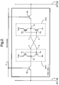
- FIG. 1 a schematic of an SRAM is shown and comprises an array of memory cells 1 arranged in 'n' rows and 'm' columns. Each memory cell 1 is capable of storing a single bit of information, that is a '0' or '1', and accordingly is often referred to as a bit cell. Data can be written to, or read from, a memory cell using a pair of bitlines 2, 3 associated with the column in which the cell is located. The required cell within the column is selected by means of a word line 4. The data values applied to the bitlines 2, 3 are the complement of each other and the present state of the cell may be read by measuring the voltage difference appearing across these lines.
- the cell 1 comprises a pair of cross-coupled inverters INV1 and INV2.
- Each inverter INV1, INV2 comprises a pmos field effect transistor (FET), Q 1 , Q 2 , respectively, and an nmos FET, Q 3 , Q 4 respectively, the pmos and nmos FET's in each inverter being connected serially.
- the inverters INV1, INV2 are cross-coupled to form a latch with output 5 of inverter INV1 connected to input 6 of inverter INV2 and output 7 of inverter INV2 connected to input 8 of inverter INV1.
- the cell 1 also contains two further nmos FET's Q 5 , Q 6 , to enable access to the cell's two interior nodes N 1 N 2 .
- the FET's Q 5 , Q 6 are controlled by means of a respective word line 4.
- the present state of the cell 1 is read by activating word line 4, that is, holding it high, to allow the voltages appearing at nodes N 1 and N 2 to affect the voltage on external bitlines 2 and 3 respectively.
- the voltage difference appearing across bitlines 2, 3 is sensed by read/write circuit means 9.
- word line 4 To write the cell to a given state word line 4 is activated and the required logic levels are applied to bitlines 2 and 3 by read/write circuit means 9 to force internal nodes N 1 and N 2 to these levels.
- the cross-coupled pair of inverters INV1, INV2 which form a latch will sustain a logic level forced on either node N 1 or N 2 indefinitely once the force is removed.
- each cell is difficult to test thoroughly, primarily due to its internal positive feedback loop and its medium impedance input/output nodes. For example, when the main feedback loop through Q 3 , Q 4 and points 5, 6, 7, 8 is not complete because of, say, a break in one of the connections between one of the inverters' outputs and the other inverter's input, then the logic levels forced into the cell by a write operation would still be held and the cell would appear to be functioning correctly. However, the levels would be stored on gate capacitance alone and would therefore only be held for a short period of time.
- High performance SRAMs use differential sensing of the voltage or current appearing on lines 2 and 3 to read the present state of the cell. Decisions as to a cell's state are made on the basis of a small, 100 mV or less, voltage difference appearing across lines 2, 3. To decrease access time required to read a cell, bit balancing or pre-charging of the bitlines is used to minimise the disturbance of the cell during a read operation. If, then, one of the cell's interior nodes N 1 or N 2 were floating on a read operation, the state of the cell may still be read correctly. However, with such a finely balanced system, the process of reading the cell's state could cause a significant disturbance within the cell, which in the absence of the positive feedback provided by the main loop would not be pulled back to the correct level. As a result the next time the cell is read its state may have changed.
- a number of other fault conditions can occur in which the feedback is single ended, that is, one of the inverters can pull the voltage of the associated node in one direction but not in the other.
- the node could sustain a low state but not a high state.
- Such a fault condition is referred to as "weak feedback" and is difficult to identify.
- the methods proposed for testing for such conditions involve increasing the cell leakage current to accelerate the problems associated with floating nodes.
- the wafer containing the cells can be irradiated with light during testing, or tests as to the long-term retention of the cells carried out at high temperatures.
- a fault condition that is particularly difficult to detect with known methods is the failure of either of the pmos transistors Q 1 , Q 2 . These transistors pull the nodes N 1 and N 2 up to the rail voltage V DD when activated thereby retaining data in the cell. They are relatively unimportant during any read or write operation and consequently detecting faults in these devices is difficult.
- a static random access memory including a circuit arrangement for detecting faults in cells of the SRAM comprising soft write means for attempting to change the state of a cell by soft writing to the cell and checking means arranged to detect if the cell flips states indicating a fault in the cell.
- cells of the memory are arranged in rows and columns with read/write means provided for reading from, or writing to cells by means of a pair of bitlines associated with each column and in which separate soft write means are provided for each bitline.
- each cell of the memory comprises a pair of cross-coupled inverters each including a pmos pull-up device
- the soft write means comprises an nmos pull-down device connected between the bitline and ground, the nmos pull-down device being weak compared to the pmos pull-up, and the circuit arrangement further including activating means to activate the weak nmos pull-down device.
- the nmos pull-down device comprises an nmos field effect transistor (FET) activated by means of a test line connected to the gate of the FET and the checking means comprises the read/write means used to read from, and write to, cells of the memory.
- FET nmos field effect transistor
- a method of detecting faults in cells of a static random access memory comprising: attempting to change the state of the cell by soft writing to the cell; and checking if the cell flips state indicating the presence of a fault in the cell.
- FIG. 3 there is shown part of an SRAM comprising a plurality of cells 1, arranged in two columns, each column containing 'n' rows.
- Each of the cells 1 comprises cross-coupled inverters as illustrated in Figure 2 and can be written to or read from using respective bitlines 2, 3 and word line 4.
- Each of the bitlines 2, 3 is switchably connected to ground by means of a respective nmos field effect transistors (FET) Q 7 , Q 8 .
- FET nmos field effect transistors
- the respective word line 4 and test line 10 are set high. Bitlines 2 and 3 are pulled towards ground potential by means of the nmos transistors Q 7 , Q 8 thereby pulling nodes N 1 N 2 of the cell under test towards ground.
- the nmos transistors Q 7 , Q 8 are selected such that they are weak in comparison to the pmos devices Q 1 , Q 2 which they are pulling against, that is Q 7 , Q 8 are less able to draw current than devices Q 1 , Q 2 .
- the effect therefore of the weak nmos transistors Q 7 , Q 8 when activated is to attempt to "soft write" the nodes of the cell to a ground.
- the pmos pull-up Q 1 associated with the other inverter INV1 can be tested in a similar manner if the cell is first set to the opposite state.
- test procedure could be to (a) write all '1's to the SRAM array, (b) activate the weak nmos pull-downs, (c) access all locations, (d) read data from all locations to check for any cells that have flipped state to a '0', (e) write all '0's to the SRAM array, (f) activate the weak nmos pull-downs, (g) access all locations and (h) read data from all locations to check for any cells that flipped to a '1'.
- testing could be applied as a variation on the memory's normal write mode, in which case the strong drivers in read/write circuit 9 used for writing would firstly have to be disabled. Due to the weakness of the pull-down nmos devices Q 7 , Q 8 , the tests may need to be carried out at reduced speed to allow time for the circuit capacitance to be overcome. For this reason, any self-timing circuits which may be present in read/write circuit 9, such circuits being provided to disable the word line access after a short period, need to be overridden. In addition any bit balancing or pre-charging circuit in read/write circuit 9 which attempts to hold the voltage of the bitlines fixed may also need to be overridden.
- Testing could also be carried out as part of the normal read access, for example the cell's state could be read as normal, the weak nmos pull-down activated and cell read once again to check if its state remains unchanged.
- An advantage of the present invention is its simplicity with only one extra gate for each bitline being required; this can be integrated as part of the SRAM very cheaply. Secondly, only a single extra test line 10 is necessary. It is envisaged that the present invention would be used in conjunction with normal testing techniques which could detect other faults that may arise in the SRAM. Whilst the present invention can detect failure of one of the pmos devices Q 1 , Q 2 in the cell, the method could fail if both pmos FET's within a given cell are faulty, since the cell will not regeneratively latch an error state. In such a situation, both interior nodes N 1 N 2 will be pulled to ground and left in this indeterminate state.
- the weak nmos pull-downs Q 7 , Q 8 can be controlled independently by separate test lines. During testing only the weak nmos pull-down associated with a node that is expected to be high is activated, thereby only loading the pmos device that is supposed to be activated.
- the means for soft writing to the cell is provided by weak nmos pull-down FET's
- other soft write means are contemplated.
- weak pmos pull-up devices could be provided to soft write the nodes of the cell to the rail voltages V DD to test the nmos FET's Q 3 and Q 4 .
- any suitable device could be selected, provided it was weak in comparison to the gate it was testing.
Landscapes
- For Increasing The Reliability Of Semiconductor Memories (AREA)
- Static Random-Access Memory (AREA)
- Testing Or Measuring Of Semiconductors Or The Like (AREA)
Applications Claiming Priority (2)
| Application Number | Priority Date | Filing Date | Title |
|---|---|---|---|
| GB9500944A GB2297173A (en) | 1995-01-18 | 1995-01-18 | Static random access memories |
| GB9500944 | 1995-01-18 |
Publications (1)
| Publication Number | Publication Date |
|---|---|
| EP0731471A1 true EP0731471A1 (fr) | 1996-09-11 |
Family
ID=10768186
Family Applications (1)
| Application Number | Title | Priority Date | Filing Date |
|---|---|---|---|
| EP95309061A Withdrawn EP0731471A1 (fr) | 1995-01-18 | 1995-12-13 | Mémoires RAM statiques |
Country Status (3)
| Country | Link |
|---|---|
| EP (1) | EP0731471A1 (fr) |
| JP (1) | JPH08263999A (fr) |
| GB (1) | GB2297173A (fr) |
Cited By (1)
| Publication number | Priority date | Publication date | Assignee | Title |
|---|---|---|---|---|
| WO2001086660A1 (fr) * | 2000-05-09 | 2001-11-15 | Koninklijke Philips Electronics N.V. | Dispositif a memoire vive statique (sram) integree et procede pour tester un tel dispositif |
Families Citing this family (3)
| Publication number | Priority date | Publication date | Assignee | Title |
|---|---|---|---|---|
| JP2000322900A (ja) | 1999-05-12 | 2000-11-24 | Mitsubishi Electric Corp | 半導体記録装置 |
| EP2057636A2 (fr) * | 2006-08-22 | 2009-05-13 | Nxp B.V. | Procédé destiné à tester une mémoire à accès aléatoire statique |
| JP2014099225A (ja) * | 2012-11-14 | 2014-05-29 | Renesas Electronics Corp | 半導体装置 |
Citations (4)
| Publication number | Priority date | Publication date | Assignee | Title |
|---|---|---|---|---|
| US4680762A (en) * | 1985-10-17 | 1987-07-14 | Inmos Corporation | Method and apparatus for locating soft cells in a ram |
| US5166608A (en) * | 1991-11-07 | 1992-11-24 | Advanced Micro Devices, Inc. | Arrangement for high speed testing of field-effect transistors and memory cells employing the same |
| US5361232A (en) * | 1992-11-18 | 1994-11-01 | Unisys Corporation | CMOS static RAM testability |
| EP0642134A2 (fr) * | 1993-09-03 | 1995-03-08 | Motorola, Inc. | Test de mémoire statique à accès aléatoire |
-
1995
- 1995-01-18 GB GB9500944A patent/GB2297173A/en not_active Withdrawn
- 1995-12-13 EP EP95309061A patent/EP0731471A1/fr not_active Withdrawn
-
1996
- 1996-01-09 JP JP8018315A patent/JPH08263999A/ja active Pending
Patent Citations (4)
| Publication number | Priority date | Publication date | Assignee | Title |
|---|---|---|---|---|
| US4680762A (en) * | 1985-10-17 | 1987-07-14 | Inmos Corporation | Method and apparatus for locating soft cells in a ram |
| US5166608A (en) * | 1991-11-07 | 1992-11-24 | Advanced Micro Devices, Inc. | Arrangement for high speed testing of field-effect transistors and memory cells employing the same |
| US5361232A (en) * | 1992-11-18 | 1994-11-01 | Unisys Corporation | CMOS static RAM testability |
| EP0642134A2 (fr) * | 1993-09-03 | 1995-03-08 | Motorola, Inc. | Test de mémoire statique à accès aléatoire |
Cited By (3)
| Publication number | Priority date | Publication date | Assignee | Title |
|---|---|---|---|---|
| WO2001086660A1 (fr) * | 2000-05-09 | 2001-11-15 | Koninklijke Philips Electronics N.V. | Dispositif a memoire vive statique (sram) integree et procede pour tester un tel dispositif |
| US6757205B2 (en) | 2000-05-09 | 2004-06-29 | Koninklijke Philips Electronics N.V. | Device with integrated SRAM memory and method of testing such a device |
| CN100423133C (zh) * | 2000-05-09 | 2008-10-01 | Nxp股份有限公司 | 包含sram存储器的集成电路及其测试方法 |
Also Published As
| Publication number | Publication date |
|---|---|
| JPH08263999A (ja) | 1996-10-11 |
| GB9500944D0 (en) | 1995-03-08 |
| GB2297173A (en) | 1996-07-24 |
Similar Documents
| Publication | Publication Date | Title |
|---|---|---|
| US11621258B2 (en) | Memory circuit and method of operating same | |
| EP0642134B1 (fr) | Test de mémoire statique à accès aléatoire | |
| US8966329B2 (en) | Fast parallel test of SRAM arrays | |
| EP1606824B1 (fr) | Test pour cellules sram faibles | |
| KR100339321B1 (ko) | 복수의메모리셀을가진메모리를구비한전자회로 | |
| DE3928410A1 (de) | Halbleiterspeichereinrichtung und testverfahren dafuer | |
| CN101065809B (zh) | 用于检测薄弱单元的sram测试方法和sram测试设备 | |
| KR100367191B1 (ko) | 테스트수단을구비한전자회로및메모리셀테스트방법 | |
| KR20050008829A (ko) | 메모리의 소프트 결함 검출 방법 및 장치 | |
| US7885093B2 (en) | Method for testing a static random access memory | |
| KR950005578B1 (ko) | 기억셀을 테스트하기 위한 회로 배열 및 그 방법 | |
| US6778450B2 (en) | Programmable weak write test mode | |
| EP0731471A1 (fr) | Mémoires RAM statiques | |
| US7239559B2 (en) | Methods and apparatus for accessing memory | |
| US20140071736A1 (en) | Testing signal development on a bit line in an sram | |
| US12080704B2 (en) | Memory cell array and method of operating same | |
| JP2009117026A (ja) | Sramのビット線スクリーニング方法 | |
| Yang et al. | Testing of latch based embedded arrays using scan tests | |
| JPH07182895A (ja) | 半導体記憶装置 | |
| EP1049104A1 (fr) | Procédé d'essai d'une ligne de bits et de circuits apparentés dans une mémoire | |
| US20090122626A1 (en) | Method and Apparatus for Selectable Guaranteed Write Through |
Legal Events
| Date | Code | Title | Description |
|---|---|---|---|
| PUAI | Public reference made under article 153(3) epc to a published international application that has entered the european phase |
Free format text: ORIGINAL CODE: 0009012 |
|
| AK | Designated contracting states |
Kind code of ref document: A1 Designated state(s): AT DE ES FR GB IT |
|
| 17P | Request for examination filed |
Effective date: 19970304 |
|
| STAA | Information on the status of an ep patent application or granted ep patent |
Free format text: STATUS: THE APPLICATION IS DEEMED TO BE WITHDRAWN |
|
| 18D | Application deemed to be withdrawn |
Effective date: 19980701 |