EP0731472A1 - Dispositif à grille anti-diffusion pour rayons-X pour la radiographie diagnostique médicale et procédé de fabrication de la grille - Google Patents
Dispositif à grille anti-diffusion pour rayons-X pour la radiographie diagnostique médicale et procédé de fabrication de la grille Download PDFInfo
- Publication number
- EP0731472A1 EP0731472A1 EP96301572A EP96301572A EP0731472A1 EP 0731472 A1 EP0731472 A1 EP 0731472A1 EP 96301572 A EP96301572 A EP 96301572A EP 96301572 A EP96301572 A EP 96301572A EP 0731472 A1 EP0731472 A1 EP 0731472A1
- Authority
- EP
- European Patent Office
- Prior art keywords
- substrate
- channels
- absorbing material
- grid
- radiation
- Prior art date
- Legal status (The legal status is an assumption and is not a legal conclusion. Google has not performed a legal analysis and makes no representation as to the accuracy of the status listed.)
- Granted
Links
Images

Classifications
-
- A—HUMAN NECESSITIES
- A61—MEDICAL OR VETERINARY SCIENCE; HYGIENE
- A61B—DIAGNOSIS; SURGERY; IDENTIFICATION
- A61B6/00—Apparatus or devices for radiation diagnosis; Apparatus or devices for radiation diagnosis combined with radiation therapy equipment
- A61B6/06—Diaphragms
-
- G—PHYSICS
- G21—NUCLEAR PHYSICS; NUCLEAR ENGINEERING
- G21K—HANDLING OF PARTICLES OR IONISING RADIATION NOT OTHERWISE PROVIDED FOR; IRRADIATION DEVICES; GAMMA RAY OR X-RAY MICROSCOPES
- G21K1/00—Arrangements for handling particles or ionising radiation, e.g. focusing or moderating
- G21K1/02—Arrangements for handling particles or ionising radiation, e.g. focusing or moderating using diaphragms, collimators
- G21K1/025—Arrangements for handling particles or ionising radiation, e.g. focusing or moderating using diaphragms, collimators using multiple collimators, e.g. Bucky screens; other devices for eliminating undesired or dispersed radiation
Definitions
- the present invention relates generally to the field of diagnostic radiography and, more particularly, to an anti-scatter grid capable of yielding high resolution, high contrast radiographic images and a method of fabricating the grid.
- x-radiation impinges upon a patient. Some of the x-radiation becomes absorbed by the patient's body, and the remainder of the x-radiation penetrates through the body. The differential absorption of the x-radiation permits the formation of a radiographic image on a photosensitive film.
- One embodiment for filtering scattered radiation includes an anti-scatter grid which is interposed between the body and the photosensitive film. Scattered radiation impinges upon absorbent (opaque) material in the grid and becomes absorbed. Also absorbed by the absorbing material, however, is a portion of the primary radiation.
- the radiographic imaging arrangement of this embodiment provides higher contrast radiographs by virtue of the elimination of the scattered radiation, but necessitates an increase in radiation dosage to the patient in order to properly expose the photographic element.
- the increased radiation requirement results in part because the scattered radiation no longer constitutes part of the imaging x-ray beam, and in part because as much as 30% or more of the primary beam impinges upon the absorbing material in the grid and itself becomes filtered out (i.e. absorbed).
- the composite of strips After the composite of strips is assembled into a stack, it must then be cut and carefully machined along its major faces to the required grid thickness that may be as thin as only 0.5 millimeters, the fragile composite then being, for example, 40 cm by 40 cm by 0.5 mm in dimension and very difficult to handle. If the stack has survived the machining and handling processes, the stack must further be laminated with sufficiently strong materials so as to reinforce the fragile grid assembly and provide enough mechanical strength for use in the field. Accidental banging, bending, or dropping of such grids can cause internal damage, i.e., delamination of the layers which cannot be repaired, rendering the grid completely useless.
- an object of an embodiment of the invention is to provide a robust anti-scatter grid with a high line rate so that it is not necessary to move the grid during an x-radiation exposure period.
- an object of an embodiment of the invention is to provide an efficient method for fabricating a robust anti-scatter grid.
- Another object of an embodiment of the invention is to provide a method for fabricating a grid with a high line rate.
- an anti-scatter x-ray grid for medical diagnostic radiography comprises a substrate having channels therein and including material that is substantially non-absorbent of x-radiation; and absorbing material in the channels including material that is substantially absorbent of x-radiation.
- the substrate comprises material capable of remaining stable at the melting temperature of the absorbing material.
- One substrate material and absorbing material combination which has been found to be particularly advantageous is a plastic substrate and a lead-bismuth alloy absorbing material.
- a method for fabricating an anti-scatter x-ray grid for medical diagnostic radiography comprises providing a substrate having channels therein and including material that is substantially non-absorbent of x-radiation; and filling the channels with absorbing material that is substantially absorbent of x-radiation.
- the step of providing a substrate having channels therein comprises sawing a plastic substrate with a thin circular blade and the step of filling the channels with absorbing material comprises melting the absorbing material and flowing the melted absorbing material into the channels.
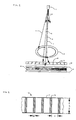
- FIG. 1 is a sectional side view of a radiographic imaging arrangement.
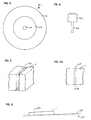
- FIG. 3 is a front view of a cutting blade.
- FIG. 4 is a sectional side view of the cutting blade of FIG. 3.
- FIG. 5 is a partial perspective view of a channel through a non-absorbent substrate.
- FIG. 5a is a sectional side view of another embodiment of a channel through a non-absorbent substrate.
- FIG. 6 is a sectional side view of a substrate support surface which is rotatable for providing the desired angle of substrate channel.
- FIG. 8 is a view similar to that of FIG. 7 after the channel has further been filled with absorbing material.
- FIG. 9 is a view similar to that of FIG. 8 after the surfaces of the substrate and absorbing material are coated with a protective layer.
- FIG. 1 is a sectional side view of a radiographic imaging arrangement.
- a tube 1 generates and emits x-radiation 2 which travels toward a body 3. Some of the x-radiation 4 is absorbed by the body while some of the radiation penetrates and travels along paths 5 and 6 as primary radiation, and other radiation is deflected and travels along path 7 as scattered radiation.
- Radiation from paths 5, 6, and 7 travels toward a photosensitive film 8 where it will become absorbed by intensifying screens 9 which are coated with a photosensitive material that fluoresces at a wavelength of visible light and thus exposes photosensitive film 8 (the radiograph) with the latent image.
- radiation paths 5, 6, and 7 travel toward the anti-scatter grid 10 before film 8.
- Radiation path 6 travels through translucent material 11 of the grid, whereas both radiation paths 5 and 7 impinge upon absorbing material 12 and become absorbed.
- the absorption of radiation path 7 constitutes the elimination of the scattered radiation.
- the absorption of radiation path 5 constitutes the elimination of part of the primary radiation.
- Radiation path 6, the remainder of the primary radiation travels toward the photosensitive film 8 and becomes absorbed by the intensifying photosensitive screens 9 that fluoresce at a wavelength of visible light and thus exposes photosensitive film 8 with the latent image.
- FIG. 2 is a sectional side view a portion of an anti-scatter x-ray grid 10.
- grid ratio r is defined as the ratio between the height h of the x-ray absorbing strips 12 and the distance d between them.
- the ratios generally range from 2:1 to 16:1.
- Another interdependent variable in the design parameters is the line rate of strips per centimeter.
- An absorbing strip must be thin enough to permit the total combined thicknesses of the strips and the distances between them to fit within a given centimeter and provide the predetermined line rate.
- line rates vary from 30 to 80 lines per centimeter and the absorbing strips have a width w along the sectional side view on the order of 15 to 50 ⁇ m. Using the present invention, higher line rates (up to about 300) can be achieved, and therefore image contrast can be improved.
- FIGS. 3 and 4 are front and sectional side views respectively of a cutting blade 21.
- FIG. 5 is a partial perspective view of a channel through a substantially non-absorbent substrate.
- an anti-scatter x-ray grid is fabricated by cutting the surface of a solid sheet of non-absorbent substrate material 11 to form the desired plurality of linear absorber channels of the desired dimensions.
- the substrate may comprise any substantially non-absorbent material having appropriate structural and thermal properties to withstand further processing and use.
- the saw may comprise a blade adapted to cut appropriately thin and deep channels in substrate 11.
- saws 21 include saws of the type used in the semiconductor industry for dicing silicon wafers such as manufactured by Tokyo Seimitsu of Japan and Semitec of Santa Clara, California, for example.
- a thin blade portion 20 extends from a thicker inner portion 22 which is rotated about an axis 24.
- the blade thickness ranges from about 15 to 70 ⁇ m so that these saws can provide desired line rates.
- the blade comprises a diamond-coated resin.
- Other materials appropriate for the saw blades include, for example, materials such as metals or resins having hard carbide coatings such as silicon or tungsten carbide.
- Either a plurality of blades can be arranged side by side to cut the channels simultaneously or a single blade can cut each of the channels sequentially. If the blade is not of sufficient depth, then one fabrication technique is to turn the substrate over and cut on the opposite surface of the substrate to form a channel having two portions 26a and 26b such as shown in FIG. 5a .
- a movable support table for use under the substrate such as available from Anorad Corporation of Hauppaugue, NY, is useful because blades for cutting semiconductor wafers are not always large enough (or do not always have enough range of motion) to create the desired length of channels.
- the channels are not limited to the rectangular shapes obtainable with the above described cutting saw.
- the channels can alternatively be round or comprise other types of cavities and can be formed by any of a number of methods such as etching, molding, heat deforming and/or reforming, milling, drilling, or any combination thereof.
- absorbing material 12 which is substantially absorbent
- substantially absorbent mean that the thickness and material density are sufficient to cause substantial attenuation of x-radiation such that at least 90% (and preferably at least 95%) of the x-radiation will be absorbed.
- the channels are filled under vacuum conditions with an absorbing material that can be readily melt-flowed into the channels.
- the absorbing material comprises a lead-bismuth alloy.
- Other substantially absorbent materials can include metals such as lead, bismuth, gold, barium, tungsten, platinum, mercury, thallium, indium, palladium, silicon, antimony, tin, zinc, and alloys thereof.
- the substrate material and absorbing material must be chosen so that the substrate material is able to withstand the temperatures required for melting and flowing the absorbing material during the amount of time required for the fabrication process.
- FIG. 7 is a sectional side view of the channel 26 coated with an optional adhesion promoting material 34.
- the adhesion promoting material can be formed on the channel surfaces.
- copper is coated to a sufficient thickness to provide a substantially continuous coating on the channel surfaces.
- Other appropriate adhesion promoting materials include nickel and iron, for example. Any residual adhesion promoting material on an outer surface of the substrate can be removed either at this time or at a later time simultaneously with residual absorbing material.
- Any residual adhesion promoting material and/or non-absorbing material remaining on the outer surfaces of the substrate can be removed by a technique such as polishing, milling, or planing, for example.
- FIG. 9 is a view similar to that of FIG. 8 after the surfaces of the substrate and absorbing material are coated with a protective layer 38.
- the protective layer may comprise similar materials as those described with respect to the substrate.
- protective layer 38 comprises a plastic such as polyetherimide.
- the protective layer comprises substantially non-absorbent material and helps to protect the substrate and absorbing material surfaces from scratches. Furthermore, the protective layer is useful for safety concerns when the absorbing material includes a metal such as lead.
- a grid prototype of a substrate comprising Ultem polyetherimide 1000 was made using a precision dicing saw where a 10 ⁇ 10 ⁇ 0.5 cm sample was cut on one face to produce channels in the surface that had a width w of 50 ⁇ m, a height h of 600 ⁇ m and a length I of 10 cm (w, h, and I shown in FIG. 5), and such that the line rate was 67 lines/cm, the lines being equally spaced to give a grid ratio of 6:1.
- the substrate was then vacuum filled with the 44% lead - 56% bismuth alloy at 140 °C by immersing the substrate into the molten metal and subjecting it to a pressure of less than 10 Torr.
- the substrate was removed and allowed to cool to ambient temperature and was then polished smooth to remove any excess or stray metal.
- the device was examined microscopically, and the channels were found to be completely and uniformly filled.
- the device of the present invention is reworkable in that the absorbing material which is not completely or properly flowed in the channels can be removed by heating the assembly and reflowing the absorbing material. Furthermore, this feature can be used to reclaim (remove) the absorbing material before later disposal of any grids. This removal capability is advantageous, especially in situations where lead may cause a safety-related concern and in situations where recycling of the substrate material is desired.
Landscapes
- Life Sciences & Earth Sciences (AREA)
- Physics & Mathematics (AREA)
- Engineering & Computer Science (AREA)
- Health & Medical Sciences (AREA)
- Medical Informatics (AREA)
- High Energy & Nuclear Physics (AREA)
- Optics & Photonics (AREA)
- Molecular Biology (AREA)
- General Engineering & Computer Science (AREA)
- Nuclear Medicine, Radiotherapy & Molecular Imaging (AREA)
- Spectroscopy & Molecular Physics (AREA)
- Pathology (AREA)
- Radiology & Medical Imaging (AREA)
- Biomedical Technology (AREA)
- Heart & Thoracic Surgery (AREA)
- Biophysics (AREA)
- Surgery (AREA)
- Animal Behavior & Ethology (AREA)
- General Health & Medical Sciences (AREA)
- Public Health (AREA)
- Veterinary Medicine (AREA)
- Apparatus For Radiation Diagnosis (AREA)
- Measurement Of Radiation (AREA)
Applications Claiming Priority (4)
| Application Number | Priority Date | Filing Date | Title |
|---|---|---|---|
| US08/402,223 US5581592A (en) | 1995-03-10 | 1995-03-10 | Anti-scatter X-ray grid device for medical diagnostic radiography |
| US402222 | 1995-03-10 | ||
| US08/402,222 US5557650A (en) | 1995-03-10 | 1995-03-10 | Method for fabricating an anti-scatter X-ray grid device for medical diagnostic radiography |
| US402223 | 1995-03-10 |
Publications (2)
| Publication Number | Publication Date |
|---|---|
| EP0731472A1 true EP0731472A1 (fr) | 1996-09-11 |
| EP0731472B1 EP0731472B1 (fr) | 2000-01-05 |
Family
ID=27017777
Family Applications (1)
| Application Number | Title | Priority Date | Filing Date |
|---|---|---|---|
| EP96301572A Expired - Lifetime EP0731472B1 (fr) | 1995-03-10 | 1996-03-07 | Dispositif à grille anti-diffusion pour rayons-X pour la radiographie diagnostique médicale et procédé de fabrication de la grille |
Country Status (7)
| Country | Link |
|---|---|
| EP (1) | EP0731472B1 (fr) |
| JP (1) | JP3851678B2 (fr) |
| KR (1) | KR100408586B1 (fr) |
| CN (1) | CN1230122C (fr) |
| DE (1) | DE69605954T2 (fr) |
| IN (1) | IN187505B (fr) |
| TW (1) | TW342325B (fr) |
Cited By (9)
| Publication number | Priority date | Publication date | Assignee | Title |
|---|---|---|---|---|
| DE19729596A1 (de) * | 1997-07-10 | 1999-01-14 | Siemens Ag | Streustrahlenraster |
| EP0911836A1 (fr) * | 1997-10-24 | 1999-04-28 | TRW Inc. | Grille réalisée avec un substrat en silicium |
| DE19839619A1 (de) * | 1998-08-31 | 1999-12-09 | Siemens Ag | Verfahren zum Herstellen eines Streustrahlenrasters und ein somit hergestelltes Streustrahlenraster eines Strahlendiagnosegerätes |
| DE19852955A1 (de) * | 1998-11-17 | 2000-05-18 | Bruker Axs Analytical X Ray Sy | Röntgenanalysegerät mit röntgenoptischem Halbleiterbauelement |
| DE19852048A1 (de) * | 1998-11-11 | 2000-05-25 | Siemens Ag | Strahlungsdetektionseinrichtung |
| WO2001073794A1 (fr) * | 2000-03-28 | 2001-10-04 | General Electric Company | Grille antidiffusion, procede associe, et appareil servant a le former |
| EP1280165A3 (fr) * | 2001-07-28 | 2008-02-13 | Philips Intellectual Property & Standards GmbH | Grille anti-diffusion pour un dispositif de rayons X |
| FR2953320A1 (fr) * | 2009-11-27 | 2011-06-03 | Gen Electric | Grille anti-diffusante inversee |
| EP3884871A4 (fr) * | 2018-12-26 | 2022-11-16 | JPI Healthcare Co., Ltd. | Procédé de fabrication d'une grille de rayons x en forme de treillis |
Families Citing this family (12)
| Publication number | Priority date | Publication date | Assignee | Title |
|---|---|---|---|---|
| JP2000217812A (ja) * | 1999-01-27 | 2000-08-08 | Fuji Photo Film Co Ltd | 散乱線除去グリッドおよびその製造方法 |
| JP2002318283A (ja) * | 2001-04-24 | 2002-10-31 | Shimadzu Corp | 2次元アレイ型放射線検出器とそのx線遮蔽壁の製造方法 |
| DE10202987A1 (de) * | 2002-01-26 | 2003-07-31 | Philips Intellectual Property | Gitter zur Absorption von Röntgenstrahlung |
| US20100006781A1 (en) * | 2006-08-25 | 2010-01-14 | Shimadzu Corporation | Hollow grid and manufacturing method thereof |
| US8331536B2 (en) * | 2009-09-18 | 2012-12-11 | General Electric Company | Apparatus for reducing scattered X-ray detection and method of same |
| KR100970910B1 (ko) * | 2010-03-19 | 2010-07-20 | (주)금성토탈퍼니처 | 침대 매트리스용 스프링조립체의 가요성 보강 구조 |
| US8265228B2 (en) * | 2010-06-28 | 2012-09-11 | General Electric Company | Anti-scatter X-ray grid device and method of making same |
| KR101333125B1 (ko) * | 2010-10-26 | 2013-11-26 | 주식회사 아임 | 엑스레이 그리드 및 그 제조방법 |
| CN103660654B (zh) * | 2012-09-13 | 2016-12-21 | 通用电气公司 | 二维准直器元件及制造二维准直器元件的方法 |
| CN105396229B (zh) * | 2015-12-28 | 2018-05-04 | 上海联影医疗科技有限公司 | 一种放射治疗设备的成像装置和方法 |
| DE102017200762A1 (de) * | 2017-01-18 | 2018-07-19 | Siemens Healthcare Gmbh | Streustrahlraster mit einem amorphen Material und dessen Verwendung bei einem Streustrahlenraster |
| CN112378933B (zh) * | 2020-10-30 | 2023-01-10 | 中建材光芯科技有限公司 | 三维聚焦玻璃基防散射滤线栅及其制造方法 |
Citations (5)
| Publication number | Priority date | Publication date | Assignee | Title |
|---|---|---|---|---|
| GB1493267A (en) * | 1975-12-03 | 1977-11-30 | Ferranti Ltd | Apparatus for collimating a beam of penetrating ionizing radiation |
| US4250127A (en) * | 1977-08-17 | 1981-02-10 | Connecticut Research Institute, Inc. | Production of electron microscope grids and other micro-components |
| US4856043A (en) * | 1988-07-18 | 1989-08-08 | North American Philips Corporation | Two piece ceramic Soller slit collimator for X-ray collimation |
| GB2273718A (en) * | 1988-11-29 | 1994-06-29 | Chromalloy Gas Turbine Corp | Preparation and coating of composite surfaces |
| US5418833A (en) * | 1993-04-23 | 1995-05-23 | The Regents Of The University Of California | High performance x-ray anti-scatter grid |
Family Cites Families (1)
| Publication number | Priority date | Publication date | Assignee | Title |
|---|---|---|---|---|
| US5231654A (en) * | 1991-12-06 | 1993-07-27 | General Electric Company | Radiation imager collimator |
-
1996
- 1996-02-26 IN IN342CA1996 patent/IN187505B/en unknown
- 1996-03-05 TW TW085102697A patent/TW342325B/zh active
- 1996-03-07 DE DE69605954T patent/DE69605954T2/de not_active Expired - Fee Related
- 1996-03-07 EP EP96301572A patent/EP0731472B1/fr not_active Expired - Lifetime
- 1996-03-08 KR KR1019960006686A patent/KR100408586B1/ko not_active Expired - Fee Related
- 1996-03-09 CN CNB961059826A patent/CN1230122C/zh not_active Expired - Fee Related
- 1996-03-11 JP JP05269896A patent/JP3851678B2/ja not_active Expired - Fee Related
Patent Citations (5)
| Publication number | Priority date | Publication date | Assignee | Title |
|---|---|---|---|---|
| GB1493267A (en) * | 1975-12-03 | 1977-11-30 | Ferranti Ltd | Apparatus for collimating a beam of penetrating ionizing radiation |
| US4250127A (en) * | 1977-08-17 | 1981-02-10 | Connecticut Research Institute, Inc. | Production of electron microscope grids and other micro-components |
| US4856043A (en) * | 1988-07-18 | 1989-08-08 | North American Philips Corporation | Two piece ceramic Soller slit collimator for X-ray collimation |
| GB2273718A (en) * | 1988-11-29 | 1994-06-29 | Chromalloy Gas Turbine Corp | Preparation and coating of composite surfaces |
| US5418833A (en) * | 1993-04-23 | 1995-05-23 | The Regents Of The University Of California | High performance x-ray anti-scatter grid |
Cited By (16)
| Publication number | Priority date | Publication date | Assignee | Title |
|---|---|---|---|---|
| DE19729596A1 (de) * | 1997-07-10 | 1999-01-14 | Siemens Ag | Streustrahlenraster |
| US6047044A (en) * | 1997-07-10 | 2000-04-04 | Siemens Aktiengesellschaft | Stray radiation grid |
| EP0911836A1 (fr) * | 1997-10-24 | 1999-04-28 | TRW Inc. | Grille réalisée avec un substrat en silicium |
| DE19839619A1 (de) * | 1998-08-31 | 1999-12-09 | Siemens Ag | Verfahren zum Herstellen eines Streustrahlenrasters und ein somit hergestelltes Streustrahlenraster eines Strahlendiagnosegerätes |
| DE19852048A1 (de) * | 1998-11-11 | 2000-05-25 | Siemens Ag | Strahlungsdetektionseinrichtung |
| DE19852955A1 (de) * | 1998-11-17 | 2000-05-18 | Bruker Axs Analytical X Ray Sy | Röntgenanalysegerät mit röntgenoptischem Halbleiterbauelement |
| DE19852955C2 (de) * | 1998-11-17 | 2000-08-31 | Bruker Axs Analytical X Ray Sy | Röntgenanalysegerät mit röntgenoptischem Halbleiterbauelement |
| US6477226B1 (en) | 1998-11-17 | 2002-11-05 | Bruker Axs Analytical X-Ray Systems Gmbh | X-ray analysis device with X-ray optical semi-conductor construction element |
| US6438210B1 (en) | 2000-03-28 | 2002-08-20 | General Electric Company | Anti-scatter grid, method, and apparatus for forming same |
| WO2001073794A1 (fr) * | 2000-03-28 | 2001-10-04 | General Electric Company | Grille antidiffusion, procede associe, et appareil servant a le former |
| US6594342B2 (en) | 2000-03-28 | 2003-07-15 | General Electric Company | Anti-scatter grid, method, and apparatus for forming same |
| KR100801118B1 (ko) * | 2000-03-28 | 2008-02-05 | 제너럴 일렉트릭 캄파니 | 산란 방지 그리드, 그 형성 방법 및 장치 |
| EP1280165A3 (fr) * | 2001-07-28 | 2008-02-13 | Philips Intellectual Property & Standards GmbH | Grille anti-diffusion pour un dispositif de rayons X |
| FR2953320A1 (fr) * | 2009-11-27 | 2011-06-03 | Gen Electric | Grille anti-diffusante inversee |
| US8666025B2 (en) | 2009-11-27 | 2014-03-04 | General Electric Company | Back focused anti-scatter grid |
| EP3884871A4 (fr) * | 2018-12-26 | 2022-11-16 | JPI Healthcare Co., Ltd. | Procédé de fabrication d'une grille de rayons x en forme de treillis |
Also Published As
| Publication number | Publication date |
|---|---|
| DE69605954T2 (de) | 2000-07-27 |
| CN1142930A (zh) | 1997-02-19 |
| TW342325B (en) | 1998-10-11 |
| DE69605954D1 (de) | 2000-02-10 |
| KR960033405A (ko) | 1996-10-22 |
| JPH08322832A (ja) | 1996-12-10 |
| CN1230122C (zh) | 2005-12-07 |
| KR100408586B1 (ko) | 2004-03-18 |
| EP0731472B1 (fr) | 2000-01-05 |
| IN187505B (fr) | 2002-05-11 |
| JP3851678B2 (ja) | 2006-11-29 |
Similar Documents
| Publication | Publication Date | Title |
|---|---|---|
| US5581592A (en) | Anti-scatter X-ray grid device for medical diagnostic radiography | |
| EP0731472B1 (fr) | Dispositif à grille anti-diffusion pour rayons-X pour la radiographie diagnostique médicale et procédé de fabrication de la grille | |
| US5557650A (en) | Method for fabricating an anti-scatter X-ray grid device for medical diagnostic radiography | |
| US6594342B2 (en) | Anti-scatter grid, method, and apparatus for forming same | |
| US6075840A (en) | Air cross grids for X-ray imaging | |
| US8666025B2 (en) | Back focused anti-scatter grid | |
| US6177237B1 (en) | High resolution anti-scatter x-ray grid and laser fabrication method | |
| WO2018063918A1 (fr) | Recuit à haute température dans la fabrication d'une source de rayons x | |
| Saitoh et al. | Characterization of sliced multilayer zone plates for hard x rays | |
| CN102187403A (zh) | 栅格以及制造用于选择性地透射电磁辐射特别是用于乳房摄影应用的x射线辐射的栅格的方法 | |
| EP0356488A1 (fr) | Filtre de reduction de rayonnement utilise dans le diagnostic medical | |
| US7430281B2 (en) | Anti-scatter grid with mechanical resistance | |
| US7286637B2 (en) | Optical thin film and mirror using the same | |
| JPH02500625A (ja) | 最小細片用ターゲツト配置 | |
| EP3140835B1 (fr) | Grille anti-diffusion de rayons x | |
| US12315647B2 (en) | Shielding mask for scattered ionizing radiation and method for production thereof | |
| JP4253737B2 (ja) | 光学部品およびその製造方法 | |
| EP2005442A1 (fr) | Procede de fabrication d'un collimateur | |
| JPH02172149A (ja) | 回転陽極x線管用ターゲツト | |
| JP2000180596A (ja) | X線用グリッド | |
| Piotrowski | 2-Dimensional primary x-ray image formation and quality in angiography using absorption-edge filters in the range 40-60 keV |
Legal Events
| Date | Code | Title | Description |
|---|---|---|---|
| PUAI | Public reference made under article 153(3) epc to a published international application that has entered the european phase |
Free format text: ORIGINAL CODE: 0009012 |
|
| AK | Designated contracting states |
Kind code of ref document: A1 Designated state(s): DE IT NL |
|
| 17P | Request for examination filed |
Effective date: 19970311 |
|
| 17Q | First examination report despatched |
Effective date: 19980403 |
|
| GRAG | Despatch of communication of intention to grant |
Free format text: ORIGINAL CODE: EPIDOS AGRA |
|
| GRAG | Despatch of communication of intention to grant |
Free format text: ORIGINAL CODE: EPIDOS AGRA |
|
| GRAH | Despatch of communication of intention to grant a patent |
Free format text: ORIGINAL CODE: EPIDOS IGRA |
|
| GRAH | Despatch of communication of intention to grant a patent |
Free format text: ORIGINAL CODE: EPIDOS IGRA |
|
| GRAA | (expected) grant |
Free format text: ORIGINAL CODE: 0009210 |
|
| AK | Designated contracting states |
Kind code of ref document: B1 Designated state(s): DE IT NL |
|
| REF | Corresponds to: |
Ref document number: 69605954 Country of ref document: DE Date of ref document: 20000210 |
|
| ITF | It: translation for a ep patent filed | ||
| PLBE | No opposition filed within time limit |
Free format text: ORIGINAL CODE: 0009261 |
|
| STAA | Information on the status of an ep patent application or granted ep patent |
Free format text: STATUS: NO OPPOSITION FILED WITHIN TIME LIMIT |
|
| 26N | No opposition filed | ||
| PGFP | Annual fee paid to national office [announced via postgrant information from national office to epo] |
Ref country code: NL Payment date: 20050216 Year of fee payment: 10 |
|
| PGFP | Annual fee paid to national office [announced via postgrant information from national office to epo] |
Ref country code: IT Payment date: 20060331 Year of fee payment: 11 |
|
| PG25 | Lapsed in a contracting state [announced via postgrant information from national office to epo] |
Ref country code: NL Free format text: LAPSE BECAUSE OF NON-PAYMENT OF DUE FEES Effective date: 20061001 |
|
| NLV4 | Nl: lapsed or anulled due to non-payment of the annual fee |
Effective date: 20061001 |
|
| PGFP | Annual fee paid to national office [announced via postgrant information from national office to epo] |
Ref country code: DE Payment date: 20070430 Year of fee payment: 12 |
|
| PG25 | Lapsed in a contracting state [announced via postgrant information from national office to epo] |
Ref country code: DE Free format text: LAPSE BECAUSE OF NON-PAYMENT OF DUE FEES Effective date: 20081001 |
|
| PG25 | Lapsed in a contracting state [announced via postgrant information from national office to epo] |
Ref country code: IT Free format text: LAPSE BECAUSE OF NON-PAYMENT OF DUE FEES Effective date: 20070307 |