EP0731492A2 - Method of growing a single crystal thin film with a uniform thickness, in the vapor phase - Google Patents
Method of growing a single crystal thin film with a uniform thickness, in the vapor phase Download PDFInfo
- Publication number
- EP0731492A2 EP0731492A2 EP96103695A EP96103695A EP0731492A2 EP 0731492 A2 EP0731492 A2 EP 0731492A2 EP 96103695 A EP96103695 A EP 96103695A EP 96103695 A EP96103695 A EP 96103695A EP 0731492 A2 EP0731492 A2 EP 0731492A2
- Authority
- EP
- European Patent Office
- Prior art keywords
- single crystal
- thin film
- crystal thin
- holder
- vapor phase
- Prior art date
- Legal status (The legal status is an assumption and is not a legal conclusion. Google has not performed a legal analysis and makes no representation as to the accuracy of the status listed.)
- Withdrawn
Links
Images



Classifications
-
- C—CHEMISTRY; METALLURGY
- C30—CRYSTAL GROWTH
- C30B—SINGLE-CRYSTAL GROWTH; UNIDIRECTIONAL SOLIDIFICATION OF EUTECTIC MATERIAL OR UNIDIRECTIONAL DEMIXING OF EUTECTOID MATERIAL; REFINING BY ZONE-MELTING OF MATERIAL; PRODUCTION OF A HOMOGENEOUS POLYCRYSTALLINE MATERIAL WITH DEFINED STRUCTURE; SINGLE CRYSTALS OR HOMOGENEOUS POLYCRYSTALLINE MATERIAL WITH DEFINED STRUCTURE; AFTER-TREATMENT OF SINGLE CRYSTALS OR A HOMOGENEOUS POLYCRYSTALLINE MATERIAL WITH DEFINED STRUCTURE; APPARATUS THEREFOR
- C30B25/00—Single-crystal growth by chemical reaction of reactive gases, e.g. chemical vapour-deposition growth
- C30B25/02—Epitaxial-layer growth
- C30B25/14—Feed and outlet means for the gases; Modifying the flow of the reactive gases
Definitions
- This invention relates in general to a method of manufacturing a single crystal thin film with a uniform thickness.
- test growth of the single crystal thin film is conducted repeatedly with different settings of the concentration, flow rates and such of said source material gas and the dopant gas until the thickness and the resistivity of said single crystal thin film achieve the desired values before manufacturing a single crystal thin film for the purpose of determining the settings of the concentration, flow rate and such of the source material gas and the dopant gas.
- the stage in which the test growth is conducted is called the preparation stage.
- the source material gas 19 is fed through the inlet ports 16 to the semiconductor single crystal substrate 12 placed on the holder 14 which is rotating on its own axis in the reactor vessel 17 of the vapor phase growth apparatus 10 and heated to the desired temperature with the heating means 15 so as to conduct a vapor phase growth of the single crystal thin film 13 on the semiconductor single crystal substrate 12, in the same manner as when manufacturing products.
- the adjustment to obtain the desired values of the thickness and resistivity of the single crystal thin film 13 it is also conducted to adjust to make sure their distribution falls within the range specified in the control standard.
- the settings of the concentration, flow rate and such of the source material gas are still adjusted in a trial-and-error fashion based on intuition and experience in the preparation stage, requiring a long preparation time and a large testing cost.
- the object of this invention is to provides a method of manufacturing a single crystal thin film which can easily achieve a uniform film thickness distribution without depending on intuition and experience.
- This invention provides a method of manufacturing a single crystal thin film which comprises vapor phase growth of a single crystal thin film on a semiconductor single crystal substrate placed on a holder for rotating on its own axis in a reactor vessel by feeding the source material gas to said semiconductor single crystal substrate, wherein growth conditions are determined by conducting a vapor phase growth of a single crystal thin film on said semiconductor single crystal substrate without rotating said holder on its axis in the preparation stage before the manufacturing of said single crystal thin film, and then said single crystal thin film is manufactured based on said growth conditions.
- Figure 1 is an explanatory cross section of the horizontal type vapor phase growth apparatus used to demonstrate the method of manufacturing a single crystal thin film pertaining to Example 1 of the present invention.
- Figure 2 is an explanatory top view of the horizontal type vapor phase growth apparatus used to demonstrate the method of manufacturing a single crystal thin film pertaining to Example 1 of the present invention.
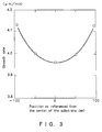
- Figure 3 is a figure showing the measurements of the growth rate at various points on a semiconductor single crystal substrate when the vapor phase growth is conducted with a conventional method while the semiconductor single crystal substrate is held stationary.
- Figure 4 is a graph showing the measurements of the growth rate at various points on a semiconductor single crystal substrate when the vapor phase growth is conducted with a method pertaining to the present invention while the semiconductor single crystal substrate is held stationary.
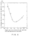
- Figure 5 is a graph showing relationship between the growth rate ratio of the left and right ends with the semiconductor single crystal substrate held stationary and the film thickness distribution with the semiconductor single crystal substrate rotated.
- Figure 6 is an explanatory cross section of the vertical type vapor phase growth apparatus used to demonstrate the method of manufacturing a single crystal thin film pertaining to Example 2 of the present invention.
- Figure 7 is an explanatory top view of the vertical type vapor phase growth apparatus used to demonstrate the method of manufacturing a single crystal thin film pertaining to Example 2 of the present invention.
- This invention provides a method of manufacturing a single crystal thin film which comprises vapor phase growth of a single crystal thin film on a semiconductor single crystal substrate placed on a holder for rotating on its own axis in a reactor vessel by feeding the source material gas to said semiconductor single crystal substrate wherein, in the preparation stage before the manufacturing of said single crystal thin film, growth conditions are determined by conducting a vapor phase growth of a single crystal thin film on said semiconductor single crystal substrate without rotating said holder on its axis and then said single crystal thin film is manufactured based on said growth conditions.
- the growth rate of the single crystal thin film should preferably be adjusted to be laterally asymmetric with respect to the virtual center axis on said holder parallel to the direction in which the source material gas is fed. Also, two growth rate measurements of said single crystal thin film taken at the right and left ends of the semiconductor crystal substrate with respect to said center axis should preferably be such that one of the growth rates is 1.3-1.8 times greater than the other.
- the vapor phase growth of the single crystal thin film is conducted on the semiconductor single crystal substrate which is held still by not allowing the holder to rotate on its own axis, and therefore the conditions of the vapor phase growth are directly reflected in the film thickness distribution of the single crystal thin film without being averaged, thus it becomes easier to determine the necessary changes in the settings for the next adjustment.
- the thickness of the single crystal thin film 13 grown on the semiconductor single crystal substrate 12 placed on said holder 14 is obtained by adding up or integrating the growth rate at each point in the path of said semiconductor single crystal substrate 12 with respect to time.
- the rotation of the semiconductor single crystal substrate 12 mentioned here means that the semiconductor single crystal substrate 12 placed on the holder 14 for rotating on its own axis rotates along with said holder 14.
- the single-wafer type growth apparatus it means it rotates on the same axis as the holder's rotating axis 11.
- the multi-wafer growth using the batch type growth apparatus it means it orbits around the same axis as the holder's rotating axis 11.
- the temperature distribution created by the heating means 15 and/or the supply rate of the source material gas 19 are adjusted in said preparation stage such that the growth rate of the single crystal thin film 13 grown with the semiconductor single crystal substrate 12 being stationary becomes laterally asymmetric with respect to the virtual center axis A on the holder 14 parallel to the feeding direction of said source material gas 19.
- the vapor phase growth of a single crystal thin film is conducted on a semiconductor single crystal substrate with the holder held stationary in the preparation stage before manufacturing a single crystal thin film, and therefore the vapor phase growth conditions are directly, without being averaged, reflected in the film thickness distribution of the single crystal thin film, making it possible to easily manufacture the single crystal thin film with a uniform film thickness distribution without depending on intuition and experience.
- the growth rate distribution on the semiconductor single crystal substrate is made asymmetric along the direction perpendicular to the feeding direction of the source material gas in said preparation stage, then large and small growth rates offset each other when said semiconductor single crystal substrate is rotated and a very uniform single crystal film thickness can be achieved.
- FIG 1 and Figure 2 are an explanatory cross section and an explanatory top view, respectively, of the horizontal type vapor phase growth apparatus used to demonstrate the method of manufacturing a single crystal thin film pertaining to Example 1 of the present invention.
- Said horizontal type vapor phase growth apparatus 10 is a single-wafer type which has a transparent quartz glass react ion vessel 17, installed horizontally, with inlet ports 16 for the source material gas 19 and an exhaust port 18, a heating means 15 placed around said reaction vessel 17 for heating the semiconductor single crystal substrate 12, a cooling means, not shown, which cools said heating means 15 and the outer wall of said reaction vessel 17 and a holder 14 for said semiconductor single crystal substrate 12.
- Said holder 14 is made of graphite coated with silicon carbide, and placed symmetrically with respect to the rotation axis 11 of the rotation drive. It can horizontally hold the semiconductor single crystal substrate 12 (a silicon single crystal substrate, for example; hereafter referred to as "silicon substrate 12") inserted in said reaction vessel 17 and rotate on its own axis.
- semiconductor single crystal substrate 12 a silicon single crystal substrate, for example; hereafter referred to as "silicon substrate 12”
- the vapor phase growth conditions were adjusted by conducting the vapor phase growth of the silicon thin film 13 on said silicon substrate 12 with said holder 14 held stationary.
- the silicon substrate 12 with a diameter of 200 mm was inserted into the reactor vessel 17 and placed on said holder 14 such that it had the same axis as the rotation axis 11 of said holder 14.
- a radiation heating lamp was used for the heating means 15 and said silicon substrate 12 was heated to the reaction temperature of 1,125°C.
- hydrogen, for the carrier gas was fed at a rate of 100 liters/minute, trichlorosilane, the source material gas, was fed horizontally at a rate of 22 g/minute from the inlet ports 16 toward the exhaust port 18 to grow the silicon thin film 13 for 1 minute.
- the flow rate distribution along the width -wise direction of the reaction vessel 17, i.e. the direction perpendicular to said center axis A, was adjusted such that the source material gas flow rate on the left side if facing to the exhaust port 18 would be approximately twice of the flow rate on the right side, and then the vapor phase growth was conducted.
- the growth rates on the left and right ends were determined by taking measurements at points 10 mm inside of the left and right ends of the silicon substrate 12 with respect to said center axis A, the growth rates were, as shown in Figure 4, 4.2 ⁇ m/minute on the left end and 3.3 ⁇ m/minute on the right end.
- the growth rate ratio of the left and right ends (hereafter referred to as the "growth rate ratio"), obtained by dividing the larger growth rate value by the smaller, was 1.3.
- the film thickness distribution with the silicon substrate rotated becomes smaller as the growth rate ratio increases.
- the film thickness distribution becomes 2% or less, and when it exceeds 1.3 the film thickness distribution becomes 1% or less.
- the film thickness distribution passes its minimum at a growth rate ratio of approximately 1.5 and then the film thickness distribution deteriorates, exceeding 1% again with a growth rate ratio over 1.8.
- FIG. 6 and Figure 7 are an explanatory cross section and an explanatory top view, respectively, of the vertical type vapor phase growth apparatus used to demonstrate the method of manufacturing a single crystal thin film pertaining to Example 2 of the present invention.
- Said vertical type vapor phase growth apparatus 20 is a batch type which has a quartz glass reaction vessel 27 with inlet ports 26 for the source material gas 29, an exhaust port 28, a holder 24 for a silicon substrate(s) 22, and a heating means 25 placed below said holder 24 for heating said silicon substrate 22.
- Said holder 24 is made of graphite coated with silicon carbide, and placed symmetrically with respect to the rotation axis 21 of the rotation drive. It can horizontally hold a plurality of the silicon substrates 22 in said reaction vessel 27 and rotate on its own axis.
- the vapor phase growth conditions were adjusted by conducting the vapor phase growth of the silicon thin film 23 on the silicon substrate 22 with said holder 24 held stationary. As shown in Figure 6 and Figure 7, four silicon substrates 22 with a diameter of 125 mm were placed on said holder 24 in the reaction vessel 27. A radiation lamp was used for the heating means 25 and said holder 24 was uniformly heated to indirectly heat said silicon substrate 22 to the reaction temperature of around 925°C.
- the source material gas 29 was vertically fed from the inlet ports 26 located on a top part of said reaction vessel to the silicon substrates 22 horizontally placed on the holder 24 and, right above the holder 24, it flowed away in the direction perpendicular to the direction in which the inlet ports 26 are lined up in series. Because of this, the film thickness distribution of the silicon thin film 23 on said holder 24 had a tendency to be thicker on the center area and thinner on the peripheral area.
- the temperature distribution on said holder 24 was adjusted such that the growth rate of the silicon thin film 23 would be laterally asymmetric with respect to the virtual center axis B on said holder 24 which is perpendicular to the direction in which said inlet ports 26 were lined up, i.e. parallel with the feeding direction of the source material gas. That is, the temperature of the area near said center axis B of the holder 24 was adjusted to be 925°C, the temperature of the area on the right side, when regarding said holder 24 from said inlet ports 26, of said center axis B was adjusted to be approximately 940 °C and the temperature of the area on the left side of said center axis B was adjusted to be approximately 910°C.
- the vapor phase growth was conducted with said holder 24 held stationary, and the growth rate distribution of the silicon thin film 23 on said holder 24 was measured.
- the growth rate was approximately 0.9 micrometers/minute on the right end with respect to said center axis B and approximately 0.6 micrometers/minute on the left end, giving a lateral growth rate ratio of 1.5.
- said holder 24 was rotated on its own axis at 35 turns/minutes and the vapor phase growth was conducted for 10 minutes to form the silicon thin film 23 with a film thickness of approximately 8 ⁇ m.
Landscapes
- Chemical & Material Sciences (AREA)
- Chemical Kinetics & Catalysis (AREA)
- General Chemical & Material Sciences (AREA)
- Engineering & Computer Science (AREA)
- Crystallography & Structural Chemistry (AREA)
- Materials Engineering (AREA)
- Metallurgy (AREA)
- Organic Chemistry (AREA)
- Crystals, And After-Treatments Of Crystals (AREA)
Abstract
In the preparation stage before the manufacturing of the single crystal thin film 13, growth conditions are determined by conducting a vapor phase growth without rotating the rotatable holder 14 on its axis and making adjustments such that the growth rate of the single crystal thin film 13 is laterally asymmetric with respect to the virtual center axis on the holder 14 parallel to the feeding direction of the source material gas 19, and then said single crystal thin film is manufactured based on said growth conditions.
Description
- This application claims the priority of Japanese Patent application No. 7-79453 filed on March 10, 1995, which are incorporeted herein by reference.
- This invention relates in general to a method of manufacturing a single crystal thin film with a uniform thickness.
- It is well known that, when conducting a vapor phase growth of a single crystal thin film by feeding the source material gas from a horizontal direction onto a semiconductor single crystal substrate horizontally placed in a horizontal-type vapor phase growth apparatus, the single crystal thin film becomes thicker on the upstream side of the source material gas flow unless said semiconductor single crystal substrate rotates. Because of this, said semiconductor single crystal substrate is rotated to average the thickness distribution of the single crystal thin film at the upstream side and at the downstream side of the source material gas flow.
- Usually, test growth of the single crystal thin film is conducted repeatedly with different settings of the concentration, flow rates and such of said source material gas and the dopant gas until the thickness and the resistivity of said single crystal thin film achieve the desired values before manufacturing a single crystal thin film for the purpose of determining the settings of the concentration, flow rate and such of the source material gas and the dopant gas. Hereafter, the stage in which the test growth is conducted is called the preparation stage.
- In said preparation stage, as shown in Figure 1 and Figure 2, the
source material gas 19 is fed through theinlet ports 16 to the semiconductorsingle crystal substrate 12 placed on theholder 14 which is rotating on its own axis in thereactor vessel 17 of the vaporphase growth apparatus 10 and heated to the desired temperature with the heating means 15 so as to conduct a vapor phase growth of the single crystalthin film 13 on the semiconductorsingle crystal substrate 12, in the same manner as when manufacturing products. In addition to the adjustment to obtain the desired values of the thickness and resistivity of the single crystalthin film 13, it is also conducted to adjust to make sure their distribution falls within the range specified in the control standard. - In recent years, due to the miniaturization of electronic device processes and enlargement of the diameter of semiconductor single crystal substrates, the thickness distribution of single crystal thin films is required to be smaller than ever. Recently, 1% or less of film thickness unevenness, as defined by equation (1), has been required.

- However, for adjustment of the film thickness distribution, the settings of the concentration, flow rate and such of the source material gas are still adjusted in a trial-and-error fashion based on intuition and experience in the preparation stage, requiring a long preparation time and a large testing cost.
- The object of this invention is to provides a method of manufacturing a single crystal thin film which can easily achieve a uniform film thickness distribution without depending on intuition and experience.
- This invention provides a method of manufacturing a single crystal thin film which comprises vapor phase growth of a single crystal thin film on a semiconductor single crystal substrate placed on a holder for rotating on its own axis in a reactor vessel by feeding the source material gas to said semiconductor single crystal substrate, wherein growth conditions are determined by conducting a vapor phase growth of a single crystal thin film on said semiconductor single crystal substrate without rotating said holder on its axis in the preparation stage before the manufacturing of said single crystal thin film, and then said single crystal thin film is manufactured based on said growth conditions.
- Figure 1 is an explanatory cross section of the horizontal type vapor phase growth apparatus used to demonstrate the method of manufacturing a single crystal thin film pertaining to Example 1 of the present invention.
- Figure 2 is an explanatory top view of the horizontal type vapor phase growth apparatus used to demonstrate the method of manufacturing a single crystal thin film pertaining to Example 1 of the present invention.
- Figure 3 is a figure showing the measurements of the growth rate at various points on a semiconductor single crystal substrate when the vapor phase growth is conducted with a conventional method while the semiconductor single crystal substrate is held stationary.
- Figure 4 is a graph showing the measurements of the growth rate at various points on a semiconductor single crystal substrate when the vapor phase growth is conducted with a method pertaining to the present invention while the semiconductor single crystal substrate is held stationary.
- Figure 5 is a graph showing relationship between the growth rate ratio of the left and right ends with the semiconductor single crystal substrate held stationary and the film thickness distribution with the semiconductor single crystal substrate rotated.
- Figure 6 is an explanatory cross section of the vertical type vapor phase growth apparatus used to demonstrate the method of manufacturing a single crystal thin film pertaining to Example 2 of the present invention.
- Figure 7 is an explanatory top view of the vertical type vapor phase growth apparatus used to demonstrate the method of manufacturing a single crystal thin film pertaining to Example 2 of the present invention.
- The present invention is further described in details below.
- This invention provides a method of manufacturing a single crystal thin film which comprises vapor phase growth of a single crystal thin film on a semiconductor single crystal substrate placed on a holder for rotating on its own axis in a reactor vessel by feeding the source material gas to said semiconductor single crystal substrate wherein, in the preparation stage before the manufacturing of said single crystal thin film, growth conditions are determined by conducting a vapor phase growth of a single crystal thin film on said semiconductor single crystal substrate without rotating said holder on its axis and then said single crystal thin film is manufactured based on said growth conditions.
- In said preparation stage, the growth rate of the single crystal thin film should preferably be adjusted to be laterally asymmetric with respect to the virtual center axis on said holder parallel to the direction in which the source material gas is fed. Also, two growth rate measurements of said single crystal thin film taken at the right and left ends of the semiconductor crystal substrate with respect to said center axis should preferably be such that one of the growth rates is 1.3-1.8 times greater than the other.
- According to this invention, in the preparation stage before manufacturing the single crystal thin film, the vapor phase growth of the single crystal thin film is conducted on the semiconductor single crystal substrate which is held still by not allowing the holder to rotate on its own axis, and therefore the conditions of the vapor phase growth are directly reflected in the film thickness distribution of the single crystal thin film without being averaged, thus it becomes easier to determine the necessary changes in the settings for the next adjustment.
- Conventionally, attempts were made to make the temperature distribution and the source material gas feeding rate uniform along the direction perpendicular to the feeding direction of said source material gas so as to make the film thickness distribution of the single crystal thin film uniform. However, the vapor
phase growth apparatus 10 shown in Figure 1 and Figure 2 was used to conduct the vapor phase growth of the single crystalthin film 13 with the semiconductorsingle crystal substrate 12 stationary and the distribution of the growth rate along the width-wise direction of thereaction vessel 17, i.e. the direction perpendicular to the virtual center axis A parallel to the feeding direction of the source material gas 9, was investigated and it was discovered that, as shown in Figure 3, the growth rate became larger in the peripheral areas of the semiconductorsingle crystal substrate 12, i.e. the areas closer to the side wall of thereaction vessel 17. When the growth rate distribution was as shown in Figure 3, the film thickness distribution obtained by rotating the semiconductorsingle crystal substrate 12 was 2.6%, as calculated using the aforementioned equation (1). - When the vapor phase growth is conducted while the
holder 14 rotates on therotation axis 11 with which theholder 14 is symmetric, the thickness of the single crystalthin film 13 grown on the semiconductorsingle crystal substrate 12 placed on saidholder 14 is obtained by adding up or integrating the growth rate at each point in the path of said semiconductorsingle crystal substrate 12 with respect to time. - The rotation of the semiconductor
single crystal substrate 12 mentioned here means that the semiconductorsingle crystal substrate 12 placed on theholder 14 for rotating on its own axis rotates along withsaid holder 14. In the single-wafer type growth apparatus, it means it rotates on the same axis as the holder's rotatingaxis 11. In the multi-wafer growth using the batch type growth apparatus, it means it orbits around the same axis as the holder's rotatingaxis 11. - That is, if the vapor phase growth is conducted with the semiconductor
single crystal substrate 12 being rotated while the temperature distribution created by the heating means 15 and the supply rate of thesource material gas 19 are made uniform along the direction perpendicular to said center axis, then the film thickness on the circumference portion of saidholder 14 inevitably becomes thicker than on the center portion, making it impossible to make the film thickness distribution of the single crystalthin film 13 uniform. - To solve this problem, the temperature distribution created by the heating means 15 and/or the supply rate of the
source material gas 19 are adjusted in said preparation stage such that the growth rate of the single crystalthin film 13 grown with the semiconductorsingle crystal substrate 12 being stationary becomes laterally asymmetric with respect to the virtual center axis A on theholder 14 parallel to the feeding direction of saidsource material gas 19. - When the single crystal
thin film 13 is grown under these conditions with the semiconductorsingle crystal substrate 12 being rotated, each point on the semiconductorsingle crystal substrate 12 repeatedly goes through areas with a large growth rate and areas with a small growth rate, so that the growth of the single crystalthin film 13 proceeds as large and small growth rates offset each other. As a result, a very uniform film thickness distribution from the center to the circumference of the semiconductorsingle crystal substrate 12 can be obtained. - According to the present invention, the vapor phase growth of a single crystal thin film is conducted on a semiconductor single crystal substrate with the holder held stationary in the preparation stage before manufacturing a single crystal thin film, and therefore the vapor phase growth conditions are directly, without being averaged, reflected in the film thickness distribution of the single crystal thin film, making it possible to easily manufacture the single crystal thin film with a uniform film thickness distribution without depending on intuition and experience.
- Also, if the growth rate distribution on the semiconductor single crystal substrate is made asymmetric along the direction perpendicular to the feeding direction of the source material gas in said preparation stage, then large and small growth rates offset each other when said semiconductor single crystal substrate is rotated and a very uniform single crystal film thickness can be achieved.
- Examples of the method of manufacturing the single crystal thin film of the present invention are described below based on Figures 1-7.
- Figure 1 and Figure 2 are an explanatory cross section and an explanatory top view, respectively, of the horizontal type vapor phase growth apparatus used to demonstrate the method of manufacturing a single crystal thin film pertaining to Example 1 of the present invention. Said horizontal type vapor
phase growth apparatus 10 is a single-wafer type which has a transparent quartz glassreact ion vessel 17, installed horizontally, withinlet ports 16 for thesource material gas 19 and anexhaust port 18, a heating means 15 placed around saidreaction vessel 17 for heating the semiconductorsingle crystal substrate 12, a cooling means, not shown, which cools said heating means 15 and the outer wall of saidreaction vessel 17 and aholder 14 for said semiconductorsingle crystal substrate 12. - Said
holder 14 is made of graphite coated with silicon carbide, and placed symmetrically with respect to therotation axis 11 of the rotation drive. It can horizontally hold the semiconductor single crystal substrate 12 (a silicon single crystal substrate, for example; hereafter referred to as "silicon substrate 12") inserted in saidreaction vessel 17 and rotate on its own axis. - First, in the preparation stage before the manufacturing of the semiconductor single crystal thin film 13 (a silicon single crystal thin film, for example; hereafter referred to as "silicon
thin film 13"), the vapor phase growth conditions were adjusted by conducting the vapor phase growth of the siliconthin film 13 on saidsilicon substrate 12 with saidholder 14 held stationary. - The
silicon substrate 12 with a diameter of 200 mm was inserted into thereactor vessel 17 and placed on saidholder 14 such that it had the same axis as therotation axis 11 ofsaid holder 14. In saidreactor vessel 17, a radiation heating lamp was used for the heating means 15 and saidsilicon substrate 12 was heated to the reaction temperature of 1,125°C. While hydrogen, for the carrier gas, was fed at a rate of 100 liters/minute, trichlorosilane, the source material gas, was fed horizontally at a rate of 22 g/minute from theinlet ports 16 toward theexhaust port 18 to grow the siliconthin film 13 for 1 minute. - When doing this, in order to make the growth rate of the silicon
thin film 13 laterally asymmetric with respect to the virtual center axis A on saidholder 14, the flow rate distribution along the width -wise direction of thereaction vessel 17, i.e. the direction perpendicular to said center axis A, was adjusted such that the source material gas flow rate on the left side if facing to theexhaust port 18 would be approximately twice of the flow rate on the right side, and then the vapor phase growth was conducted. - As a result, when the growth rates on the left and right ends were determined by taking measurements at
points 10 mm inside of the left and right ends of thesilicon substrate 12 with respect to said center axis A, the growth rates were, as shown in Figure 4, 4.2 µm/minute on the left end and 3.3 µm/minute on the right end. The growth rate ratio of the left and right ends (hereafter referred to as the "growth rate ratio"), obtained by dividing the larger growth rate value by the smaller, was 1.3. - Under these vapor phase growth conditions, said
holder 14 was rotated on its own axis at 35 r.p.m. and the vapor phase growth of the siliconthin film 13 was conducted. The resulting film thickness distribution, calculated by using the aforementioned equation (1), was 1.0%. - Similar testing was conducted by adjusting the flow rate distribution along the width-wise direction of the
reaction vessel 17 with a supply rate of hydrogen, the carrier gas, in the range of 40-100 liters/minute and a supply rate of trichlorosilane, the source material gas, in the range of 5-22 g/minute. The relationship between the growth rate ratio with thesilicon substrate 12 held stationary and the film thickness distribution with thesilicon substrate 12 rotated was experimentally determined and the results are shown in Figure 5. - As shown in Figure 5, the film thickness distribution with the silicon substrate rotated becomes smaller as the growth rate ratio increases. When the growth rate ratio exceeds approximately 1.1, the film thickness distribution becomes 2% or less, and when it exceeds 1.3 the film thickness distribution becomes 1% or less. However, when the growth rate ratio is increased further, the film thickness distribution passes its minimum at a growth rate ratio of approximately 1.5 and then the film thickness distribution deteriorates, exceeding 1% again with a growth rate ratio over 1.8.
- Figure 6 and Figure 7 are an explanatory cross section and an explanatory top view, respectively, of the vertical type vapor phase growth apparatus used to demonstrate the method of manufacturing a single crystal thin film pertaining to Example 2 of the present invention. Said vertical type vapor
phase growth apparatus 20 is a batch type which has a quartzglass reaction vessel 27 withinlet ports 26 for the sourcematerial gas 29, anexhaust port 28, aholder 24 for a silicon substrate(s) 22, and a heating means 25 placed below saidholder 24 for heating saidsilicon substrate 22. - Said
holder 24 is made of graphite coated with silicon carbide, and placed symmetrically with respect to therotation axis 21 of the rotation drive. It can horizontally hold a plurality of thesilicon substrates 22 in saidreaction vessel 27 and rotate on its own axis. - First, the vapor phase growth conditions were adjusted by conducting the vapor phase growth of the silicon
thin film 23 on thesilicon substrate 22 with saidholder 24 held stationary. As shown in Figure 6 and Figure 7, foursilicon substrates 22 with a diameter of 125 mm were placed on saidholder 24 in thereaction vessel 27. A radiation lamp was used for the heating means 25 and saidholder 24 was uniformly heated to indirectly heat saidsilicon substrate 22 to the reaction temperature of around 925°C. - While hydrogen, for the carrier gas, was fed into said
reactor vessel 27 at a rate of 100 liters/minute, trichlorosilane, the source material gas, was fed vertically at a rate of 22 g/minute from theinlet ports 26, arranged in series, to saidsilicon substrate 22, as shown in Figure 7, to grow the siliconthin film 23 for 10 minutes. - The source
material gas 29 was vertically fed from theinlet ports 26 located on a top part of said reaction vessel to thesilicon substrates 22 horizontally placed on theholder 24 and, right above theholder 24, it flowed away in the direction perpendicular to the direction in which theinlet ports 26 are lined up in series. Because of this, the film thickness distribution of the siliconthin film 23 on saidholder 24 had a tendency to be thicker on the center area and thinner on the peripheral area. - Considering this tendency, the temperature distribution on said
holder 24 was adjusted such that the growth rate of the siliconthin film 23 would be laterally asymmetric with respect to the virtual center axis B on saidholder 24 which is perpendicular to the direction in which saidinlet ports 26 were lined up, i.e. parallel with the feeding direction of the source material gas. That is, the temperature of the area near said center axis B of theholder 24 was adjusted to be 925°C, the temperature of the area on the right side, when regarding saidholder 24 from saidinlet ports 26, of said center axis B was adjusted to be approximately 940 °C and the temperature of the area on the left side of said center axis B was adjusted to be approximately 910°C. - Under the aforementioned reaction conditions, the vapor phase growth was conducted with said
holder 24 held stationary, and the growth rate distribution of the siliconthin film 23 on saidholder 24 was measured. As a result, the growth rate was approximately 0.9 micrometers/minute on the right end with respect to said center axis B and approximately 0.6 micrometers/minute on the left end, giving a lateral growth rate ratio of 1.5. Under these vapor phase growth conditions, saidholder 24 was rotated on its own axis at 35 turns/minutes and the vapor phase growth was conducted for 10 minutes to form the siliconthin film 23 with a film thickness of approximately 8 µm. The film thickness distribution, calculated by using the aforementioned equation (1), was 0.8 %. - Similar testing was further conducted and as a result the film thickness distribution similarly became 1% or less when the growth rate ratio of the left and right ends became 1.3 or more, and the film thickness distribution when said
holder 24 was rotated was further reduced as the growth rate ratio of the left and right ends increased. However, when the temperature of the left side, when facing to thesilicon substrate 22, of said center axis B was reduced even further to increase the growth rate ratio of the left and right ends, unevenness called "microroughness" appeared to develop on the surface of the siliconthin film 23 when the growth rate ratio of the left and right ends became 2.0 or more.
Claims (3)
- A method of manufacturing a single crystal thin film which comprises vapor phase growth of a single crystal thin film on a semiconductor single crystal substrate placed on a holder for rotating on its own axis in a reactor vessel by feeding the source material gas to said semiconductor single crystal substrate:wherein growth conditions are determined by conducting a vapor phase growth of a single crystal thin film on said semiconductor single crystal substrate without rotating said holder on its axis in the preparation stage before the manufacturing of said single crystal thin film; and thensaid single crystal thin film is manufactured based on said growth conditions.
- The method of manufacturing a single crystal thin film of Claim 1 wherein, in said preparation stage, the growth rate of the single crystal thin film is adjusted to be laterally asymmetric with respect to the virtual center axis on said holder parallel to the direction in which the source material gas is fed.
- The method of manufacturing a single crystal thin film of Claim 2 wherein two growth rate measurements of said single crystal thin film taken at the right and left ends of the semiconductor crystal substrate with respect to said center axis are such that one of the growth rates is 1.3-1.8 times greater than the other.
Applications Claiming Priority (2)
| Application Number | Priority Date | Filing Date | Title |
|---|---|---|---|
| JP79453/95 | 1995-03-10 | ||
| JP7079453A JPH08250430A (en) | 1995-03-10 | 1995-03-10 | Manufacture of single-crystal thin film |
Publications (2)
| Publication Number | Publication Date |
|---|---|
| EP0731492A2 true EP0731492A2 (en) | 1996-09-11 |
| EP0731492A3 EP0731492A3 (en) | 1998-04-08 |
Family
ID=13690305
Family Applications (1)
| Application Number | Title | Priority Date | Filing Date |
|---|---|---|---|
| EP96103695A Withdrawn EP0731492A3 (en) | 1995-03-10 | 1996-03-08 | Method of growing a single crystal thin film with a uniform thickness, in the vapor phase |
Country Status (3)
| Country | Link |
|---|---|
| US (1) | US5685905A (en) |
| EP (1) | EP0731492A3 (en) |
| JP (1) | JPH08250430A (en) |
Cited By (3)
| Publication number | Priority date | Publication date | Assignee | Title |
|---|---|---|---|---|
| EP0794561A1 (en) * | 1996-03-04 | 1997-09-10 | Shin-Etsu Handotai Company Limited | Method of growing a silicon single crystal thin film in vapor phase |
| US5759263A (en) * | 1996-12-05 | 1998-06-02 | Abb Research Ltd. | Device and a method for epitaxially growing objects by cvd |
| DE19845252A1 (en) * | 1998-10-01 | 2000-04-06 | Deutsche Telekom Ag | Process for the production of semiconductor layers |
Families Citing this family (2)
| Publication number | Priority date | Publication date | Assignee | Title |
|---|---|---|---|---|
| JP3516654B2 (en) * | 2000-12-27 | 2004-04-05 | 信越半導体株式会社 | Vapor phase growth apparatus and method for manufacturing epitaxial wafer |
| JP2006173482A (en) * | 2004-12-17 | 2006-06-29 | Hitachi Kokusai Electric Inc | Semiconductor device manufacturing method and substrate processing apparatus |
Family Cites Families (8)
| Publication number | Priority date | Publication date | Assignee | Title |
|---|---|---|---|---|
| DE1444502B2 (en) * | 1963-08-01 | 1970-01-08 | IBM Deutschland Internationale Büro-Maschinen OmbH, 7032 Sindelfingen | Process for controlling the sharpness of pn junctions to be formed on gallium arsenide single crystals |
| US4147571A (en) * | 1977-07-11 | 1979-04-03 | Hewlett-Packard Company | Method for vapor epitaxial deposition of III/V materials utilizing organometallic compounds and a halogen or halide in a hot wall system |
| JPS61248518A (en) * | 1985-04-26 | 1986-11-05 | Oki Electric Ind Co Ltd | Manufacturing equipment for compound semiconductor thin film |
| FR2591616A1 (en) * | 1985-12-17 | 1987-06-19 | Labo Electronique Physique | REACTOR CHAMBER FOR EPITAXIAL GROWTH IN STEAM PHASE OF SEMICONDUCTOR MATERIALS. |
| JPH0616491B2 (en) * | 1986-04-07 | 1994-03-02 | 日本電気株式会社 | Vapor phase epitaxial growth system |
| US4719124A (en) * | 1986-07-28 | 1988-01-12 | American Telephone And Telegraph Company At&T Bell Laboratories | Low temperature deposition utilizing organometallic compounds |
| US5456205A (en) * | 1993-06-01 | 1995-10-10 | Midwest Research Institute | System for monitoring the growth of crystalline films on stationary substrates |
| JP2605604B2 (en) * | 1993-11-24 | 1997-04-30 | 日本電気株式会社 | Method for epitaxial growth of semiconductor crystal and molecular beam supply device used for the method |
-
1995
- 1995-03-10 JP JP7079453A patent/JPH08250430A/en active Pending
-
1996
- 1996-03-07 US US08/612,393 patent/US5685905A/en not_active Expired - Fee Related
- 1996-03-08 EP EP96103695A patent/EP0731492A3/en not_active Withdrawn
Cited By (4)
| Publication number | Priority date | Publication date | Assignee | Title |
|---|---|---|---|---|
| EP0794561A1 (en) * | 1996-03-04 | 1997-09-10 | Shin-Etsu Handotai Company Limited | Method of growing a silicon single crystal thin film in vapor phase |
| US5868833A (en) * | 1996-03-04 | 1999-02-09 | Shin-Etsu Handotai Co., Ltd. | Method of producing silicon single crystal thin film |
| US5759263A (en) * | 1996-12-05 | 1998-06-02 | Abb Research Ltd. | Device and a method for epitaxially growing objects by cvd |
| DE19845252A1 (en) * | 1998-10-01 | 2000-04-06 | Deutsche Telekom Ag | Process for the production of semiconductor layers |
Also Published As
| Publication number | Publication date |
|---|---|
| EP0731492A3 (en) | 1998-04-08 |
| JPH08250430A (en) | 1996-09-27 |
| US5685905A (en) | 1997-11-11 |
Similar Documents
| Publication | Publication Date | Title |
|---|---|---|
| US4388342A (en) | Method for chemical vapor deposition | |
| US6110290A (en) | Method for epitaxial growth and apparatus for epitaxial growth | |
| JP3888059B2 (en) | Vapor growth equipment | |
| US3854443A (en) | Gas reactor for depositing thin films | |
| US5487358A (en) | Apparatus for growing silicon epitaxial layer | |
| EP0837495B1 (en) | Vapor phase growth apparatus | |
| US20070281084A1 (en) | Apparatus and method for depositing layer on substrate | |
| EP0743379A1 (en) | Apparatus for vapor-phase epitaxial growth | |
| US5755878A (en) | Method for vapor phase growth | |
| US6746941B2 (en) | Semiconductor wafer and production method therefor | |
| KR100765866B1 (en) | Thin film vapor phase growth method and thin film vapor phase growth apparatus used in the method | |
| JP7230877B2 (en) | Epitaxial wafer manufacturing system and epitaxial wafer manufacturing method | |
| TW202300696A (en) | Control device and control method for single-wafer type epitaxial growth device, and epitaxial wafer manufacturing system | |
| US5685905A (en) | Method of manufacturing a single crystal thin film | |
| US5654230A (en) | Method of forming doped film | |
| EP0031671B1 (en) | A method of growing silicate glass layers employing a chemical vapour deposition process | |
| US5743956A (en) | Method of producing single crystal thin film | |
| JP3788836B2 (en) | Vapor growth susceptor and manufacturing method thereof | |
| EP4200462A1 (en) | Window for chemical vapor deposition systems and related methods | |
| JPS6090894A (en) | Vapor phase growing apparatus | |
| JPH05259082A (en) | Epitaxial growth apparatus and epitaxial growth method | |
| JP2004134625A (en) | Semiconductor device manufacturing method and manufacturing apparatus | |
| GB2395492A (en) | Improvements in deposition methods for the production of semiconductors | |
| JP3113478B2 (en) | Semiconductor manufacturing equipment | |
| EP4711508A1 (en) | Sic epitaxial wafer |
Legal Events
| Date | Code | Title | Description |
|---|---|---|---|
| PUAI | Public reference made under article 153(3) epc to a published international application that has entered the european phase |
Free format text: ORIGINAL CODE: 0009012 |
|
| AK | Designated contracting states |
Kind code of ref document: A2 Designated state(s): DE FR GB |
|
| PUAL | Search report despatched |
Free format text: ORIGINAL CODE: 0009013 |
|
| AK | Designated contracting states |
Kind code of ref document: A3 Designated state(s): DE FR GB |
|
| 17P | Request for examination filed |
Effective date: 19980429 |
|
| STAA | Information on the status of an ep patent application or granted ep patent |
Free format text: STATUS: THE APPLICATION IS DEEMED TO BE WITHDRAWN |
|
| 18D | Application deemed to be withdrawn |
Effective date: 20000903 |