EP0732422B1 - Substrat revêtu d'une couche mince ferroélectrique, méthode pour sa fabrication et mémoire rémanente comprenant ce substrat - Google Patents
Substrat revêtu d'une couche mince ferroélectrique, méthode pour sa fabrication et mémoire rémanente comprenant ce substrat Download PDFInfo
- Publication number
- EP0732422B1 EP0732422B1 EP96301577A EP96301577A EP0732422B1 EP 0732422 B1 EP0732422 B1 EP 0732422B1 EP 96301577 A EP96301577 A EP 96301577A EP 96301577 A EP96301577 A EP 96301577A EP 0732422 B1 EP0732422 B1 EP 0732422B1
- Authority
- EP
- European Patent Office
- Prior art keywords
- film
- thin
- ferroelectric
- ferroelectric thin
- growth layer
- Prior art date
- Legal status (The legal status is an assumption and is not a legal conclusion. Google has not performed a legal analysis and makes no representation as to the accuracy of the status listed.)
- Expired - Lifetime
Links
- 239000010409 thin film Substances 0.000 title claims description 406
- 239000000758 substrate Substances 0.000 title claims description 86
- 238000000034 method Methods 0.000 title claims description 48
- 230000015654 memory Effects 0.000 title claims description 27
- 238000004519 manufacturing process Methods 0.000 title claims description 26
- 239000010936 titanium Chemical group 0.000 claims description 177
- GWEVSGVZZGPLCZ-UHFFFAOYSA-N Titan oxide Chemical compound O=[Ti]=O GWEVSGVZZGPLCZ-UHFFFAOYSA-N 0.000 claims description 37
- OGIDPMRJRNCKJF-UHFFFAOYSA-N titanium oxide Inorganic materials [Ti]=O OGIDPMRJRNCKJF-UHFFFAOYSA-N 0.000 claims description 37
- 239000000463 material Substances 0.000 claims description 31
- 230000008569 process Effects 0.000 claims description 24
- 239000013078 crystal Substances 0.000 claims description 23
- 238000010438 heat treatment Methods 0.000 claims description 15
- 238000002488 metal-organic chemical vapour deposition Methods 0.000 claims description 14
- 229910052797 bismuth Inorganic materials 0.000 claims description 11
- JCXGWMGPZLAOME-UHFFFAOYSA-N bismuth atom Chemical compound [Bi] JCXGWMGPZLAOME-UHFFFAOYSA-N 0.000 claims description 10
- 239000000126 substance Substances 0.000 claims description 10
- 239000010410 layer Substances 0.000 description 126
- 230000010287 polarization Effects 0.000 description 53
- BASFCYQUMIYNBI-UHFFFAOYSA-N platinum Substances [Pt] BASFCYQUMIYNBI-UHFFFAOYSA-N 0.000 description 30
- VYPSYNLAJGMNEJ-UHFFFAOYSA-N Silicium dioxide Chemical compound O=[Si]=O VYPSYNLAJGMNEJ-UHFFFAOYSA-N 0.000 description 28
- 229910052814 silicon oxide Inorganic materials 0.000 description 28
- 230000002269 spontaneous effect Effects 0.000 description 27
- 239000002994 raw material Substances 0.000 description 24
- 239000003990 capacitor Substances 0.000 description 17
- 230000005684 electric field Effects 0.000 description 14
- 239000007789 gas Substances 0.000 description 14
- 238000002441 X-ray diffraction Methods 0.000 description 10
- XUIMIQQOPSSXEZ-UHFFFAOYSA-N Silicon Chemical compound [Si] XUIMIQQOPSSXEZ-UHFFFAOYSA-N 0.000 description 8
- 230000000694 effects Effects 0.000 description 8
- 238000003754 machining Methods 0.000 description 8
- 229910052710 silicon Inorganic materials 0.000 description 8
- 239000010703 silicon Substances 0.000 description 8
- 229910052719 titanium Inorganic materials 0.000 description 8
- 239000012790 adhesive layer Substances 0.000 description 7
- 229910004356 Ti Raw Inorganic materials 0.000 description 6
- RTAQQCXQSZGOHL-UHFFFAOYSA-N Titanium Chemical compound [Ti] RTAQQCXQSZGOHL-UHFFFAOYSA-N 0.000 description 6
- 230000008859 change Effects 0.000 description 6
- 238000003980 solgel method Methods 0.000 description 6
- 230000015572 biosynthetic process Effects 0.000 description 5
- 238000006243 chemical reaction Methods 0.000 description 5
- 230000005621 ferroelectricity Effects 0.000 description 5
- 239000000203 mixture Substances 0.000 description 5
- 239000012071 phase Substances 0.000 description 5
- 239000004065 semiconductor Substances 0.000 description 5
- XKRFYHLGVUSROY-UHFFFAOYSA-N Argon Chemical compound [Ar] XKRFYHLGVUSROY-UHFFFAOYSA-N 0.000 description 4
- 229910052581 Si3N4 Inorganic materials 0.000 description 4
- 239000012159 carrier gas Substances 0.000 description 4
- 230000001747 exhibiting effect Effects 0.000 description 4
- 230000003647 oxidation Effects 0.000 description 4
- 238000007254 oxidation reaction Methods 0.000 description 4
- 229910052697 platinum Inorganic materials 0.000 description 4
- 229910021420 polycrystalline silicon Inorganic materials 0.000 description 4
- 238000004151 rapid thermal annealing Methods 0.000 description 4
- 238000004544 sputter deposition Methods 0.000 description 4
- VXUYXOFXAQZZMF-UHFFFAOYSA-N titanium(IV) isopropoxide Chemical compound CC(C)O[Ti](OC(C)C)(OC(C)C)OC(C)C VXUYXOFXAQZZMF-UHFFFAOYSA-N 0.000 description 4
- 230000008901 benefit Effects 0.000 description 3
- 239000000919 ceramic Substances 0.000 description 3
- 230000006866 deterioration Effects 0.000 description 3
- 238000009792 diffusion process Methods 0.000 description 3
- 238000001704 evaporation Methods 0.000 description 3
- 238000005259 measurement Methods 0.000 description 3
- 239000000376 reactant Substances 0.000 description 3
- 238000005245 sintering Methods 0.000 description 3
- 229910003781 PbTiO3 Inorganic materials 0.000 description 2
- 229910052786 argon Inorganic materials 0.000 description 2
- 239000011248 coating agent Substances 0.000 description 2
- 238000000576 coating method Methods 0.000 description 2
- 239000002131 composite material Substances 0.000 description 2
- 230000003247 decreasing effect Effects 0.000 description 2
- 238000005530 etching Methods 0.000 description 2
- 230000006870 function Effects 0.000 description 2
- 108010067216 glycyl-glycyl-glycine Proteins 0.000 description 2
- 230000010354 integration Effects 0.000 description 2
- 229910052751 metal Inorganic materials 0.000 description 2
- 239000002184 metal Substances 0.000 description 2
- 239000007769 metal material Substances 0.000 description 2
- 239000005365 phosphate glass Substances 0.000 description 2
- 238000002360 preparation method Methods 0.000 description 2
- 230000001737 promoting effect Effects 0.000 description 2
- XLUBVTJUEUUZMR-UHFFFAOYSA-B silicon(4+);tetraphosphate Chemical compound [Si+4].[Si+4].[Si+4].[O-]P([O-])([O-])=O.[O-]P([O-])([O-])=O.[O-]P([O-])([O-])=O.[O-]P([O-])([O-])=O XLUBVTJUEUUZMR-UHFFFAOYSA-B 0.000 description 2
- 229910052715 tantalum Inorganic materials 0.000 description 2
- GZXOHHPYODFEGO-UHFFFAOYSA-N triglycine sulfate Chemical compound NCC(O)=O.NCC(O)=O.NCC(O)=O.OS(O)(=O)=O GZXOHHPYODFEGO-UHFFFAOYSA-N 0.000 description 2
- QNRATNLHPGXHMA-XZHTYLCXSA-N (r)-(6-ethoxyquinolin-4-yl)-[(2s,4s,5r)-5-ethyl-1-azabicyclo[2.2.2]octan-2-yl]methanol;hydrochloride Chemical compound Cl.C([C@H]([C@H](C1)CC)C2)CN1[C@@H]2[C@H](O)C1=CC=NC2=CC=C(OCC)C=C21 QNRATNLHPGXHMA-XZHTYLCXSA-N 0.000 description 1
- MYMOFIZGZYHOMD-UHFFFAOYSA-N Dioxygen Chemical compound O=O MYMOFIZGZYHOMD-UHFFFAOYSA-N 0.000 description 1
- 229910001218 Gallium arsenide Inorganic materials 0.000 description 1
- 229910003327 LiNbO3 Inorganic materials 0.000 description 1
- 229910012463 LiTaO3 Inorganic materials 0.000 description 1
- 230000006978 adaptation Effects 0.000 description 1
- 239000000853 adhesive Substances 0.000 description 1
- 230000001070 adhesive effect Effects 0.000 description 1
- 230000002411 adverse Effects 0.000 description 1
- 229910045601 alloy Inorganic materials 0.000 description 1
- 239000000956 alloy Substances 0.000 description 1
- QVGXLLKOCUKJST-UHFFFAOYSA-N atomic oxygen Chemical compound [O] QVGXLLKOCUKJST-UHFFFAOYSA-N 0.000 description 1
- 229910002113 barium titanate Inorganic materials 0.000 description 1
- 230000004888 barrier function Effects 0.000 description 1
- 229910002115 bismuth titanate Inorganic materials 0.000 description 1
- 238000003776 cleavage reaction Methods 0.000 description 1
- 239000004020 conductor Substances 0.000 description 1
- 238000002425 crystallisation Methods 0.000 description 1
- 230000008025 crystallization Effects 0.000 description 1
- 238000005520 cutting process Methods 0.000 description 1
- 230000007547 defect Effects 0.000 description 1
- 238000010586 diagram Methods 0.000 description 1
- 239000003989 dielectric material Substances 0.000 description 1
- 229910001882 dioxygen Inorganic materials 0.000 description 1
- 239000007772 electrode material Substances 0.000 description 1
- 230000008020 evaporation Effects 0.000 description 1
- 239000007792 gaseous phase Substances 0.000 description 1
- 238000000227 grinding Methods 0.000 description 1
- 230000006872 improvement Effects 0.000 description 1
- 230000006698 induction Effects 0.000 description 1
- 238000009413 insulation Methods 0.000 description 1
- 239000012212 insulator Substances 0.000 description 1
- 239000011229 interlayer Substances 0.000 description 1
- 238000005468 ion implantation Methods 0.000 description 1
- 150000002500 ions Chemical class 0.000 description 1
- 238000002156 mixing Methods 0.000 description 1
- 231100000989 no adverse effect Toxicity 0.000 description 1
- 230000003287 optical effect Effects 0.000 description 1
- 230000001590 oxidative effect Effects 0.000 description 1
- 239000001301 oxygen Substances 0.000 description 1
- 229910052760 oxygen Inorganic materials 0.000 description 1
- 239000002245 particle Substances 0.000 description 1
- 238000001259 photo etching Methods 0.000 description 1
- 230000003252 repetitive effect Effects 0.000 description 1
- 230000007017 scission Effects 0.000 description 1
- HQVNEWCFYHHQES-UHFFFAOYSA-N silicon nitride Chemical compound N12[Si]34N5[Si]62N3[Si]51N64 HQVNEWCFYHHQES-UHFFFAOYSA-N 0.000 description 1
- 238000009751 slip forming Methods 0.000 description 1
- GUVRBAGPIYLISA-UHFFFAOYSA-N tantalum atom Chemical compound [Ta] GUVRBAGPIYLISA-UHFFFAOYSA-N 0.000 description 1
- XOLBLPGZBRYERU-UHFFFAOYSA-N tin dioxide Chemical compound O=[Sn]=O XOLBLPGZBRYERU-UHFFFAOYSA-N 0.000 description 1
- 229910001887 tin oxide Inorganic materials 0.000 description 1
- 238000001771 vacuum deposition Methods 0.000 description 1
- 238000007740 vapor deposition Methods 0.000 description 1
- 238000005019 vapor deposition process Methods 0.000 description 1
Images


Classifications
-
- C—CHEMISTRY; METALLURGY
- C23—COATING METALLIC MATERIAL; COATING MATERIAL WITH METALLIC MATERIAL; CHEMICAL SURFACE TREATMENT; DIFFUSION TREATMENT OF METALLIC MATERIAL; COATING BY VACUUM EVAPORATION, BY SPUTTERING, BY ION IMPLANTATION OR BY CHEMICAL VAPOUR DEPOSITION, IN GENERAL; INHIBITING CORROSION OF METALLIC MATERIAL OR INCRUSTATION IN GENERAL
- C23C—COATING METALLIC MATERIAL; COATING MATERIAL WITH METALLIC MATERIAL; SURFACE TREATMENT OF METALLIC MATERIAL BY DIFFUSION INTO THE SURFACE, BY CHEMICAL CONVERSION OR SUBSTITUTION; COATING BY VACUUM EVAPORATION, BY SPUTTERING, BY ION IMPLANTATION OR BY CHEMICAL VAPOUR DEPOSITION, IN GENERAL
- C23C16/00—Chemical coating by decomposition of gaseous compounds, without leaving reaction products of surface material in the coating, i.e. chemical vapour deposition [CVD] processes
- C23C16/22—Chemical coating by decomposition of gaseous compounds, without leaving reaction products of surface material in the coating, i.e. chemical vapour deposition [CVD] processes characterised by the deposition of inorganic material, other than metallic material
- C23C16/30—Deposition of compounds, mixtures or solid solutions, e.g. borides, carbides, nitrides
- C23C16/40—Oxides
-
- C—CHEMISTRY; METALLURGY
- C23—COATING METALLIC MATERIAL; COATING MATERIAL WITH METALLIC MATERIAL; CHEMICAL SURFACE TREATMENT; DIFFUSION TREATMENT OF METALLIC MATERIAL; COATING BY VACUUM EVAPORATION, BY SPUTTERING, BY ION IMPLANTATION OR BY CHEMICAL VAPOUR DEPOSITION, IN GENERAL; INHIBITING CORROSION OF METALLIC MATERIAL OR INCRUSTATION IN GENERAL
- C23C—COATING METALLIC MATERIAL; COATING MATERIAL WITH METALLIC MATERIAL; SURFACE TREATMENT OF METALLIC MATERIAL BY DIFFUSION INTO THE SURFACE, BY CHEMICAL CONVERSION OR SUBSTITUTION; COATING BY VACUUM EVAPORATION, BY SPUTTERING, BY ION IMPLANTATION OR BY CHEMICAL VAPOUR DEPOSITION, IN GENERAL
- C23C16/00—Chemical coating by decomposition of gaseous compounds, without leaving reaction products of surface material in the coating, i.e. chemical vapour deposition [CVD] processes
- C23C16/02—Pretreatment of the material to be coated
- C23C16/0272—Deposition of sub-layers, e.g. to promote the adhesion of the main coating
Definitions
- the present invention refers to a ferroelectric thin-film coated substrate used in a ferroelectric memory element, a pyroelectric sensor element, a piezoelectric element and the like, and a manufacturing method thereof and the nonvolatile memory comprising a ferroelectric thin-film coated substrate.
- ferroelectrics are applied to a wide development of devices such as capacitor, oscillator, optical modulator or infrared sensor. So far, for use in these applications, single crystal, such as triglycine sulfate (TGS), LiNbO 3 and LiTaO 3 or sintered ceramics such as BaTiO 3 , PbTiO 3 , Pb(Zr 1-x Ti x )O 3 (PZT) and PLZT, ferroelectric material, has been machined to the order of 50 ⁇ m in thickness by cutting and grinding.
- TGS triglycine sulfate
- LiNbO 3 and LiTaO 3 LiTaO 3
- sintered ceramics such as BaTiO 3 , PbTiO 3 , Pb(Zr 1-x Ti x )O 3 (PZT) and PLZT
- ferroelectric nonvolatile memories FLC
- Ferroelectric nonvolatile memories need no backup power supply by making use of a ferroelectric characteristic (hysteresis effect) of ferroelectrics.
- oxide ferroelectrics such as PbTiO 3 , PZT and PLZT into a thin-film by the thin-film forming method such as sputtering, evaporation, sol-gel process and MOCVD.
- PZT Pb(Zr 1-x Ti x ) O 3
- Y1 is a Bi-based layered oxide material, expressed in chemical formula SrBi 2 Ta 2 O 9 , and produced by MOD process.
- the MOD process is a thin-film forming method comprising the following steps. As with the sol-gel process, organic metal materials are mixed to form a predetermined thin-film composition and a material solution for coating with the concentration and the viscosity adjusted is prepared. This solution is spin coated to the ground plate, dried and provisionally sintered. These steps are repeated till the thin-film has reached a predetermined thickness and finally the crystallization by a true sintering is accomplished. Accordingly, control of the thin-film thickness is restricted by the thickness of a one-time coated thin-film (cf. 1994 Autumn Applied Physics Meeting Preprints, 20p-M-19).
- the sintering temperature is extremely high as 750°C to 800°C and a further long sintering time of an hour or longer is necessary. That is because, when the steps of thin-film formation and heat treatment are performed at 650°C or higher temperatures for a long period of time in such production process, a mutual diffusion reaction between the underlying platinum electrode and ferroelectrics and further a reaction between silicon or silicon oxide below the underlying electrode and ferroelectrics take place, and a change in thin-film composition due to the volatilization of component element from the ferroelectrics thin-film occurs, so that application to the actual production process of devices becomes difficult.
- oxide ferroelectrics not containing Pb adversely affecting the leak current and resistance to polarization inversion include a group of bismuth based oxide ferroelectrics having layered crystal structures expressed in the following general chemical formula.
- A is selected from Na 1+ , K 1+ , Pb 2+ , Ca 2+ , Sr 2+ , Ba 2+ , Bi 3+ and the like
- B is selected from Fe 3+ , Ti 4+ , Nb 5+ , Ta 5+ , W 6+ and Mo 6+
- m is an integer not less than 1.
- Their crystal structure have a fundamental structure in which a layered perovskite layer in an array of perovskite lattices composed of (m-1) ABO 3 is sandwiched by two layers of (Bi 2 O 2 ) 2+ from above and from below.
- Sr, Ba or Bi as A with Ti, Ta or Nb as B exhibit ferroelectricity.
- the above Y1 is one type of these bismuth based oxide ferroelectrics.
- Bi 4 Ti 3 O 12 bismuth titanate
- a c-axis oriented Bi 4 Ti 3 O 12 thin-film is prepared at substrate temperatures of 600°C or higher on a Pt/SiO 2 /Si substrate or on a Pt substrate, but these substrates cannot be directly applied to an actual device structure. That is, as with the Pt/Ti/SiO 2 /Si substrate, an adhesive layer, such as Ti layer, for ensuring the adhesive strength between the Pt electrode layer and its underlying SiO 2 layer is necessary.
- the thin-film surface morphology comprises coarse crystal grains
- application to a highly integrated device requiring a fine machining is impossible and moreover pin holes are still more apt to be caused for the thinner thin-film and consequently occurrence of leak current is induced.
- the pyrochlore phase exhibits no ferroelectricity, mixing of the pyrochlore phase leads to deterioration of ferroelectricity on the whole thin-film.
- the above prior art has a problem that, in applying a ferroelectric thin-film to highly integrated devices, those satisfactorily meeting the denseness and the evenness of the surface of a thin-film required for fine machining or low leak current, a large residual spontaneous polarization, and various requirements for the low-temperature thin-film forming process are not yet obtained.
- a ferroelectric substrate having a dense and even surface and a large residual spontaneous polarization which can be prepared in the low-temperature thin-film forming process, and the manufacture method thereof, and a nonvolatile memory composed thereof.
- the present invention provides a ferroelectric thin-film coated substrate as set out in claim 1.
- the layered crystal structure expressed in a chemical formula Bi 2 A m-1 B m O 3m+3 where A is selected from Na 1+ , K 1+ , Pb 2+ , Ca 2+ , Sr 2+ , Ba 2+ , Bi 3+ and the like, B is selected from Fe 3+ , Ti 4+ , Nb 5+ , Ta 5+ , W 6+ and Mo 6+ , and m is an integer not less than 1, is a crystal structure formed by the alternate stacking of (Bi 2 O 2 ) 2+ layers and (A m-1 B m O 3m+3 ) 2- layers.
- selection of A and B here is not limited to a single way.
- Typical of ferroelectric materials having such a crystal structure is Bi 4 Ti 3 O 12 .
- others are SrBi 2 Nb 2 O 9 , SrBi 2 Ta 2 O 9 , Babi 2 Nb 2 O 9 , BaBi 2 Ta 2 O 9 , Pb 2 Bi 2 Nb 2 O 9 , PbBi 2 Ta 2 O 9 , SrBi 4 Ti 4 O 15 , BaBi 4 Ti 4 O 15 , PbBi 4 Ti 4 O 15 , Na 0.5 B i4.5 Ti 4 O 15 , K 0.5 Bi 4.5 Ti 4 O 15 , Sr 2 Bi 4 Ti 5 O 18 , Ba 2 Bi 4 Ti 5 O 18 and Pb 2 Bi 4 Ti 5 O 18 .
- ferroelectric materials expressed in the same chemical formula, having a layered crystal structure and exhibiting no ferroelectric characteristic include Bi 3 TiNbO 9 , Bi 3 TiTaO 9 , CaBi 2 Nb 2 O 9 , CaBi 2 Ta 2 O 9 and CaBi 4 Ti 4 O 15 .
- Ferroelectric thin-film coated substrates made by forming ferroelectric thin-films composed of these bismuth-based oxide ferroelectric materials on a substrate, the interposition of both a buffer layer and a growth layer for allowing the ferroelectric thin-film to grow between the substrate and the ferroelectric thin-film enables a marked upgrade in crystallinity, ferroelectricity, electrical properties, thin-film properties and the like.
- the present invention can be thought to be effective for those dielectric materials expressed in the above-mentioned chemical formula Bi 2 A m-1 B m O 3m+3 having a layered crystal structure similar to that of a Bi 4 Ti 3 O 12 as the ferroelectric thin-film.
- the growth layer since those indicating a crystal structure resembling that of a ferroelectric thin-film is thought to be preferable, those composed of oxide materials containing the component elements of a ferroelectric thin-film or bismuth-based oxide materials having a layered structure similar to that of a ferroelectric thin-film can be regarded as preferable.
- the buffer layer those composed of the component elements of the ferroelectric thin-film and the growth layer can be regarded as preferable.
- the invention also provides a method for manufacturing a ferroelectric thin film coated substrate as set out in claim 4.
- the invention further provides a method for manufacturing a ferroelectric thin-film coated substrate as set out in claim 8.
- a random orientation thin-film of Bi 4 Ti 3 O 12 ferroelectric thin-film could be formed by forming a growth layer (Bi 4 Ti 3 O 12 thin-film) at thin-film forming temperatures of 400°C to 650°C and a Bi 4 Ti 3 O 12 ferroelectric thin-film at lower temperatures of 300°C to 400°C than the growth layer forming temperature. Furthermore, by controlling the thin-film forming temperature of the growth layer (Bi 4 Ti 3 O 12 thin-film) within the range of 400°C to 650°C, the crystallinity (orientation) of a ferroelectric thin-film was found to be controllable.
- a Bi 4 Ti 3 O 12 ferroelectric thin-film can be formed at by far lower temperatures of 300°C to 400°C than the conventional thin-film forming temperature, a very dense and smooth thin-film can be implemented.
- the above thin-film forming process can be performed at the temperature of 650°C or less, it is very effectively applied to a highly integrated device.
- the randomly oriented component can be intensified and the residual spontaneous polarization of a ferroelectric thin-film can be very greatly increased as compared with a conventional one by effectively utilizing the a-axis oriented component of Bi 4 Ti 3 O 12 .
- the heat treatment step after such a thin-film forming step as mentioned above, the crystallinity of a ferroelectric thin-film can be further enhanced, the residual spontaneous polarization can be increased and the leak current characteristic can be noticeably improved.
- the heat treatment temperature is effective in the range of 500°C to 700°C, and since the effect is obtained by a short-time treatment even around 700°C, no adverse effect is exerted even on a highly integrated device in application.
- capacitor-structured nonvolatile memories according to the present invention can exhibit a sufficient characteristic.
- MFMIS-FET-structured nonvolatile memories according to the present invention can exhibit a sufficient characteristic.
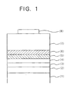
- FIG. 1 shows the structure of a ferroelectrics thin-film substrate according to a first embodiment of the present invention.
- this ferroelectric thin-film coated substrate comprises a silicon oxide (SiO 2 ) layer 2, an adhesive layer 3, a lower electrode layer 4, a buffer layer 5, c growth layer for allowing a ferroelectrics thin-film to grow 6, a ferroelectric thin-film 7 and an upper electrode layer 8 successively formed on a silicon (Si) substrate 1.
- a silicon single crystal wafer was employed as the silicon substrate 1, while a silicon oxide thin-film obtained by thermally oxidizing the surface of the silicon single crystal wafer was employed as the SiO 2 layer 2.
- a tantalum (Ta) thin-film, a platinum (Pt) thin-film, a titanium oxide thin-film, a Bi 4 Ti 3 O 12 thin-film, a Bi 4 Ti 3 O 12 thin-film and a platinum (Pt) thin-film are employed as the adhesive layer 3, the lower electrode layer 4, a buffer layer 5, a growth layer 6, a ferroelectric thin-film 7 and an upper electrode layer 8, respectively.
- a Pt/Ta/SiO 2 /Si substrate By thermal oxidation of the surface of (100) plane in a silicon single crystal wafer as the silicon substrate 1, a SiO 2 layer 2, 200 nm in thin-film thickness, is formed. Then, a Ta thin-film as the adhesive layer 3, 30 nm in thin-film thickness, and a Pt thin-film as the lower electrode layer 4, 200 nm in thin-film thickness, are formed respectively by the sputter method.
- these materials and the thin-film thickness are not limited to this arrangement, but a polycrystalline silicon substrate, a GaAs substrate or the like may be also employed.
- the adhesive layer is provided for preventing the peeling of a thin-film from occurring during the thin-film forming due to a difference in thermal expansion coefficient between the substrate and the lower electrode layer, the thin-film thickness is only necessary to be as thick as capable of preventing the peeling of a thin-film.
- Other materials such as titanium (Ti) than Ta may be employed, but Ta is preferable because Ti and Pt form an alloy.
- the SiO 2 layer employed for the insulating layer may not be prepared by heat treatment, an SiO 2 thin-film, a silicon nitride thin-film or the like are formed by the sputtering process, the vapor deposition process and the like. Any material and any thin-film thickness are allowable so long as a sufficient insulation is ensured.
- the thin-film thickness is only required to be as large as equal to the function of an electrode and the material is not limited to Pt but may be metal materials employed for ordinary electrode materials and can be appropriately selected in relation to other thin-film.
- a thin-film formation method is also not limited to the silicon oxidation process or the sputtering process heretofore and ordinary thin-film forming techniques such as vapor deposition may be employed.
- the structure of a substrate is also not limited to the above-mentioned.
- titanium isopropoxide Ti(i-OC 3 H 7 ) 4
- Ti(i-OC 3 H 7 ) 4 titanium isopropoxide
- the flow rate at the Ar gas supply was set at 100 sccm.
- Pt/Ta/SiO 2 /Si substrate prepared as described above heated and kept at a definite temperature in the thin-film forming chamber a 5 nm thick titanium oxide thin-film was formed on this substrate. At that time, the time taken for the forming step of a titanium oxide was of the order of 30 sec.
- Table 1 shows the supply conditions of raw materials for the thin-film forming by the MOCVD process at this time.
- the flow rate of Ar gas at the supply was set at 200 sccm for Bi raw material and 100 sccm for Ti raw material, while the flow rate of O 2 gas at the supply was set at 1000 sccm.
- the degree of vacuum in the thin-film forming chamber was set at 5 Torr, because the gaseous phase reaction is apt to occur if it is above 1333 Pa (10 Torr).
- the thin-film forming temperature i.e., the substrate temperature at 450°C and 500°C
- two kinds of samples 50 nm in the total thickness of a titanium oxide buffer layer and a Bi 4 Ti 3 O 12 thin-film (growth layer)
- the thin-film thickness of Bi 4 Ti 3 O 12 thin-film (growth layer) was set at 45 nm, and was made rather larger at any rate for purposes of observing the surface morphology and the crystallinity.
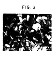
- a control was also prepared in which no titanium oxide buffer layer was formed and a Bi 4 Ti 3 O 12 thin-film was formed directly on the Pt/Ta/SiO 2 /Si substrate in a thickness of 150 nm. Except that no titanium oxide buffer layer was formed and the thin-film forming temperature was set at 500°C, the thin-film forming conditions for this control are quite the same as with the samples mentioned above.
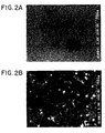
- FIGs. 2A, 2B and 3 show the SEM observed results
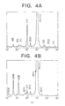
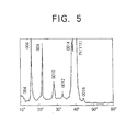
- Figs 4A, 4B and 5 shows the observed results on X-ray diffractometer.
- FIGs. 2A and 4A relate to samples of 450°C
- FIGs. 2B and 4B relate to samples of 500°C, respectively.
- FIGs. 3 and 5 show the respective observed results of controls without titanium oxide buffer layer.
- the thin-film forming up to the Bi 4 Ti 3 O 12 thin-film of growth layer is carried out in quite the same manner as that described above except for setting the thickness of a Bi 4 Ti 3 O 12 thin-film of growth layer to 5 nm. Also in this case, two types of samples were prepared setting the thin-film forming temperature (the substrate temperature) of a Bi 4 Ti 3 O 12 thin-film (growth layer) at 450°C and 500°C. The time taken for the thin-film forming step of a Bi 4 Ti 3 O 12 thin-film growth layer was around 30 sec for any sample.
- the thin-film forming conditions for a Bi 4 Ti 3 O 12 of ferroelectric thin-film are quite the same as those of a Bi 4 Ti 3 O 12 thin-film of growth layer described using Table 1.
- the time taken for the thin-film forming step of a Bi 4 Ti 3 O 12 thin-film of ferroelectric thin-film was around 30 min for any sample, and therefore the time taken for the thin-film forming step of a buffer layer, a growth layer and a ferroelectric thin-film is nearly equal to 30 min in total for any sample.
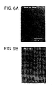
- FIGs. 6A and 6B show the observed results under SEM, while FIGs. 7A and 7B show the observed results on X-ray diffractometer.
- FIGs. 6A and 7A relate to samples of 450°C and FIGs. 6B and 7B relate to samples of 500°C.
- this arrangement showed only the results for the thin-film forming temperature of the growth layer of 450°C and for that of 500°C, but it could be confirmed that the thin-film forming temperature ranging from 400°C to 650°C permits a sufficiently smooth and dense crystallinity of growth layer (Bi 4 Ti 3 O 12 thin-film) to be obtained. Furthermore, at thin-film forming temperature of not lower than 650°C, though the crystallinity is high, the growth of crystalline grains was so much that no smooth-surface growth layer (Bi 4 Ti 3 O 12 thin-film) could be obtained.
- a Bi 4 Ti 3 O 12 of ferroelectric thin-film according to an embodiment of the present invention exhibits a very dense, smooth and good thin-film surface morphology and forms a random orientation thin-film containing components other than that of the c-axis orientation. Furthermore, it was found that those of 450°C in the thin-film forming temperature (substrate temperature) of the Bi 4 Ti 3 O 12 thin-film exhibit a denser and smoother surface morphology than those of 500°C and are superior in random orientation regarding crystallinity.
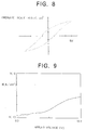
- Such a capacitor structure as shown in FIG. 1 was constructed by forming an upper electrode layer on the ferroelectric thin-film (Bi 4 Ti 3 O 12 thin-film) for two types of samples prepared in this manner and the electric characteristic of this thin-film was estimated, where a 100 ⁇ m ⁇ Pt electrode thin-film was formed as this electrode by vacuum deposition process.
- a sample with the growth layer (Bi 4 Ti 3 O 12 thin-film) formed at 450°C exhibits such a ferroelectric hysteresis curve as shown in FIG. 8.
- FIG. 10 shows the ferroelectric hysteresis curve of a still another sample of this arrangement, i.e., a sample with the growth layer (Bi 4 Ti 3 O 12 thin-film) formed at 500°C.
- Pr is smaller than Pr of FIG. 8
- Ec is also smaller than Ec of FIG. 8.
- This is attributable to a strong c-axis oriented component though the crystallinity of this sample is a random orientation.
- Such a small value of Ec suggests that the sample is applicable to a device operable at low voltage.
- the thin-film forming temperature of a Bi 4 Ti 3 O 12 of growth layer was set at 450°C, a sample having a 40 nm thick Bi 4 Ti 3 O 12 of ferroelectric thin-film and having a 50 nm thick composite of titanium oxide buffer layer and growth layer was prepared. Except that the thickness of a Bi 4 Ti 3 O 12 of ferroelectric thin-film was set at 40 nm, the preparing method was quite the same as with the first embodiment. At that time, the time taken for the step of forming a Bi 4 Ti 3 O 12 ferroelectric thin-film was around 15 min and therefore the time taken for the steps of forming a buffer layer, a growth layer and ferroelectric layer is approximately 15 min in total.
- the ferroelectric hysteresis curve of a sample according to this embodiment obtained from a measurement similar to that of the first embodiment is shown in FIG. 11.
- the repetitive fatigue for polarization inversion was measured on a sample according to this embodiment
- the test conditions are that, when repeatedly applying a pair of bipolar pulses at an applied voltage of 3V and in a pulse width of 100 ns, the changing rate of switching charge quantity (difference between the inversion charge quantity and the non-inversion charge quantity of polarization) is measured.
- the results are shown in FIG. 12.
- a decrease in switching charge quantity is about 13% after 1 ⁇ 10 12 times of repetitions and accordingly the fatigue resistance of this arrangement is clearly by far superior since that of a conventional PZT material is at most on the order of 10 8 .
- FIG. 13 shows the observed results of thin-film surface morphology under SEM in this arrangement. Since the thin-film is thin, this sample comprises fine crystalline grains on the order of nm and a good characteristic of very dense and smooth thin-film was found to be obtained.
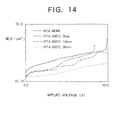
- a third embodiment with heat treatment applied to a sample prepared according to the second embodiment will be described.
- the RTA Rapid Thermal Annealing
- high-speed heat treatment by infrared irradiation was applied at a heat treatment temperature of 650°C in oxygen gas flow and the ferroelectric characteristic was examined for different periods of treatment time of 2 min, 10 min and 30 min.
- leak current Il varies depending on applied voltage as shown in FIG.14.
- RTA treatment time With longer RTA treatment time, Il was markedly improved. This is attributable to an improvement in the crystallinity of a Bi 4 Ti 3 O 12 of ferroelectric thin-film due to heat treatment in this arrangement.
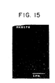
- a sample having a 190 nm thick Bi 4 Ti 3 O 12 ferroelectric thin-film and having a 200 nm composite of titanium oxide buffer layer and growth layer (Bi 4 Ti 3 O 12 ) was prepared. Except that the thin-film forming temperature of a growth layer (Bi 4 Ti 3 O 12 thin-film) was set at 450°C, the preparing method was quite the same as that of the first and second embodiments. At that time, the time taken for the step of forming a Bi 4 Ti 3 O 12 ferroelectric thin-film was of the order of 60 min and therefore the time taken for the steps of forming a buffer layer, a growth layer and ferroelectrics layer is approximately of the order of an hour in total.
- FIG. 15 shows the result of SEM observation of thin-film surface morphology in this embodiment.
- a very dense, smooth and good thin-film surface morphology on the order of 10 nm is exhibited.
- the thin-film thickness was nearly double that of the first embodiment, the surface morphology of the Bi 4 Ti 3 O 12 ferroelectric thin-film is found to be strongly affected by the growth layer (Bi 4 Ti 3 O 12 thin-film).
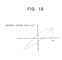
- FIG. 16 shows the ferroelectric hysteresis curve of a sample according to this embodiment, measured as with the above embodiments.
- the present invention could be confirmed to be effective for as thick a ferroelectric thin-film as 200 nm.
- the thickness was set at 5 nm for any of titanium oxide layer and growth layer (Bi 4 Ti 3 O 12 thin-film) but the present invention was significantly obtained even if the thickness of either layer is within the range of 3 nm to 10 nm.
- this embodiment employed a Pt lower electrode layer/Ta adhesive layer/SiO 2 insulating layer/Si substrate as the substrate, but, in spite of a former report that the pyrochlore phase of Bi 4 Ti 3 O 12 was apt to occur when a Bi 2 Ti 2 O 7 thin-film is formed on a similar substrate by low-temperature forming through aids of the MOCVD process, it was proved that no pyrochlore phase of Bi 2 Ti 2 O 7 occurs in this embodiment and the present invention is not limited to such a substrate structure.
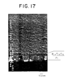
- FIGs. 17 and 18 show the surface morphology and sectional shape of this Bi 4 Ti 3 O 12 thin-film by perspective SEM photography and the X-ray diffraction pattern of this Bi 4 Ti 3 O 12 thin-film.
- a thin-film according to the fifth embodiment is a good crystallinity Bi 4 Ti 3 O 12 thin-film, so-called random orientation thin-film comprising the c-axis (00n) and (117) oriented components and a dense and smooth thin-film.
- the peak intensity ratio of this embodiment was proved to be situated just between that of FIG. 7A and that of FIG. 7B. From this it is considered that the orientation state of a Bi 4 Ti 3 O 12 according to this embodiment is an intermediate state between that shown in FIG. 7A and that shown in FIG. 7B.
- FIG. 21 the measured result of fatigue resistance in the relevant Bi 4 Ti 3 O 12 thin-film is shown in FIG. 21.
- a change in residual polarization was such a degree that about 3.2% decrease of Pr was noticed after 1 ⁇ 10 12 times of repetitions and accordingly the fatigue characteristic of ferroelectric thin-films according to embodiments of the present invention is proved to be extremely excellent as compared with a conventional PZT material (the fatigue resistance limit is below 10 8 times).
- a sixth embodiment will be described hereinafter.
- a Bi 4 Ti 3 O 12 ferroelectric thin-film was formed so as to obtain a total thickness of 50 nm.
- FIG. 22 shows the surface morphology and sectional shape of this Bi 4 Ti 3 O 12 thin-film by perspective SEM photography.
- a dense, smooth-surface, good crystallinity and random orientation Bi 4 Ti 3 O 12 thin-film was obtained.
- a sufficient ferroelectric characteristic can be effectively drawn out by using a very thin-film as 50 nm thick thin-film, which is the most important merit also in application to a large capacity FRAM or the like.
- a seventh embodiment will be described hereinafter.
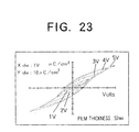
- a 5 nm thick Bi 4 Ti 3 O 12 growth layer was formed subsequently by simultaneously supplying a Bi raw material, a Ti raw material and O 2 gas at a substrate temperature of 450°C.
- a Bi 4 Ti 3 O 12 thin-film 100 nm in total thickness, was prepared by simultaneously supplying a Bi raw material, a Ti raw material and O 2 gas again under the same conditions and in the same quantity as with the forming of the Bi 4 Ti 3 O 12 .
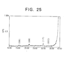
- FIGs. 24 and 25 shown the surface morphology and sectional shape of this Bi 4 Ti 3 O 12 thin-film by perspective SEM photography and the X-ray diffraction pattern of this Bi 4 Ti 3 O 12 thin-film.
- a thin-film according to the fifth embodiment is a good crystallinity Bi 4 Ti 3 O 12 thin-film, so-called random orientation thin-film comprising the c-axis (00n) and (117) oriented components and a dense and smooth thin-film.
- the crystallinity was not so good, use of the present invention enables a Bi 4 Ti 3 O 12 thin-film to be grown even at very low substrate temperature of 300°C.
- a ferroelectric thin-film (Bi 4 Ti 3 O 12 thin-film) exhibiting a good ferroelectric characteristic was obtained at a thin-film forming temperature ranging from 400°C to 650°C for a titanium oxide buffer layer and a growth layer (Bi 4 Ti 3 O 12 thin-film) by the MOCVD process.
- a ferroelectric thin-film (Bi 4 Ti 3 O 12 thin-film) having a strong c-axis orientation and exhibiting a large residual spontaneous polarization Pr was obtained.
- a good ferroelectric characteristic was exhibited at a thin-film forming of a ferroelectric thin-film (Bi 4 Ti 3 O 12 thin-film) by the MOCVD process within the temperature range of 300°C to 400°C.
- the heat treatment in a production method according to the present invention exhibits a significant effect in the temperature range of 500°C to 700°C and a sufficient effect can be obtained for a short period of time even at temperatures around 700°C, so that the present invention is sufficiently applicable also to a highly integrated device.
- conditions of materials, supplied gas or the like except the thin-film forming temperature are not limited to those of the embodiments mentioned above but are appropriately set dependently on a thin-film forming device, supplied gas and the like.
- the thin-film forming temperature of a titanium oxide buffer layer is set equal to that of a Bi 4 Ti 3 O 12 of growth layer considering the productivity, because a change in substrate temperature lengthens the manufacturing time of a device in actual manufacturing steps.
- the thin-film forming temperature of a titanium oxide buffer layer may be set different from that of a Bi 4 Ti 3 O 12 of growth layer.
- FIGs. 26A and 26B show an embodiment wherein to a nonvolatile memory of capacitor structure is made use of the Bi 4 Ti 3 O 12 ferroelectric thin-film mentioned above and the equivalent circuit thereof, respectively.
- a nonvolatile memory of capacitor structure in which use is made of the ferroelectric thin-films shown in these embodiments comprises a capacitor 108 and a transistor 107.
- a capacitor 108 comprises a ⁇ 117> oriented Bi 4 Ti 3 O 12 thin-film 5 and a pair of conductors (electrodes) 110 and 110' sandwiching
- a transistor 107 comprises a bit line 112, a word line 111 and a signal line 113 connected to an AI electrode 109.
- the AI electrode 109 is connected also to the electrode 110' of the capacitor 108.
- a method for producing aforesaid capacitor-structured nonvolatile memory will be described.
- photo-etching is conducted in such a manner that Si 3 N 4 remains at the site on which to form a transistor and field oxidation is effected to form a field SiO 2
- Poly-Si gate 111 is formed.
- a source 112 and a drain 113 are formed by ion implantation with this gate 111 used as a mask, then covering these structures with PSG (silicon phosphate glass) as the interlayer insulating thin-film and making the whole surface even by reflow.
- PSG silicon phosphate glass
- an electrode 110 After forming an electrode 110 thereon, a ⁇ 117> oriented Bi 4 Ti 3 O 12 thin-film 105 and an electrode 110' are formed in sequence. Then, after forming the structures with PSG again and effecting a reflow, contact holes are formed on the electrode 110' and the drain 113 by etching and finally an AI electrode 109 for wiring is provided.
- the ⁇ 117> oriented Bi 4 Ti 3 O 12 thin-film 105 mentioned here is that formed at a thin-film forming temperature of 450°C in the first embodiment mentioned above.
- the ⁇ 117> oriented Bi 4 Ti 3 O 12 thin-film 105 was formed after forming the titanium oxide buffer layer and the growth layer, not shown in FIG. 26A, on the electrode 110 under conditions similar to those of the first embodiment.
- the reason for using a ⁇ 117> oriented Bi 4 Ti 3 O 12 thin-film as the ferroelectric thin-film is that a thin-film exhibiting a large residual spontaneous polarization is preferable in this embodiment.
- the ferroelectric thin-film 105 is polarized and a positive residual polarization charge is stored on the side of the electrode 110 of the capacitor 108.
- this memory device is allowed to operate normally as a DRAM and as a nonvolatile memory only at the OFF period of power supply.
- FIG. 27 shows a sectional structural schematic illustration of this embodiment.
- MFMIS-FET Metal Ferroelectric Metal Insulator Semiconductor-Field Effect Transistor
- the PSG on the PPt gate 115 is removed by etching, a c-axis oriented Bi 4 Ti 3 O 12 ferroelectric thin-film 116 is formed thereon and further a control gate 117 is formed with Pt. Then, after covering these structures with PSG again and effecting a reflow, contact holes are formed on the control gate 117, the drain 119 and the source 120 and finally AI electrodes 118, 121 and 122 for wiring are provided.
- the c-axis oriented Bi 4 Ti 3 O 12 thin-film 116 mentioned here is that formed at a thin-film forming temperature of 500°C for the titanium oxide and the growth layer in the first embodiment mentioned above.
- a c-axis oriented Bi 4 Ti 3 O 12 thin-film 116 was formed after forming the titanium oxide buffer layer and the growth layer not shown in FIG. 27 under conditions similar to those of the first embodiment.
- a c-axis oriented Bi 4 Ti 3 O 12 thin-film is employed as the ferroelectric thin-film.
- the SiO 2 114 of gate insulating is dielectrically polarized via the floating gate 115 by its electrostatic induction and the direction of polarization changes. Since the formation of a channel on the semiconductor surface directly beneath the gate can be controlled by this direction of polarization, "0" and "1" can be defined by the ON-OFF of drain current. That is, assume that, at the zero bias state of the gate electrode, the ferroelectric thin-film 116 is so polarized in the direction of the semiconductor substrate that the side of the floating gate 115 becomes negative. In this case, the SiO 2 114 is dielectrically polarized, its surface in contact with the Si substrate 101 becomes positive, so that the drain 119 and the source 120 are disconnected (OFF state).
- the ferroelectric thin-film 116 inverts the polarization direction and is so polarized that the side of the floating gate 115 becomes positive.
- the SiO 2 114 is dielectrically polarized and its surface in contact with the Si substrate 101 becomes positive, whereas the surface of the Si substrate 101 in contact with the SiO 2 114 becomes negative, so that the drain 119 and the source 120 is connected (ON state). In this state, even when making the gate voltage into a zero bias state, this ON state is maintained by the residual polarization.
- this arrangement can operate as a nonvolatile memory allowing a nondestructive readout.
- a quite excellent ferroelectric characteristic can be obtained in a large value of residual spontaneous polarization and a high reliability can be implemented in excellent leak current characteristic and fatigue resistance.
- a very large value of 16 ⁇ C/cm 2 in residual spontaneous polarization can be obtained and a sufficient ferroelectric characteristic can be obtained even for a approx. 50 nm thick thin-film.
- This advantage enables a sufficient polarization charge to be ensured even when forming a infinitesimal-sized capacitor and accordingly is effective for application to a highly integrated device.
- a very dense and smooth thin-film morphology is obtained, various fine machining processes can be coped with and therefore this advantage is also effective for the application to a highly integrated device.
- a ferroelectric thin-film coated substrate manufacturing method since a ferroelectric thin-film of random orientation thin-film can be obtained and its orientation (crystallinity) can be controlled, the residual spontaneous polarization and the reacting electric field can be controlled dependently on a device to be applied and the degree of freedom can be greatly promoted. And, since the producing step can be carried out at a low temperature, various conventional devices such as a highly integrated device troublesome in high-temperature process can be coped with. Forming a coated thin-film by using the MOCVD process, not a conventional MOD or sol-gel process, enables a large-area thin-film to be produced with a good controllability at high speed, thereby promoting the productivity significantly.
- a capacitor-structured nonvolatile memory according to the present invention permit a sufficient characteristic to be obtained as the nonvolatile memory.
- an MFMIS-FET-structured nonvolatile memory permits a sufficient characteristic to be obtained as the nonvolatile memory.
Landscapes
- Chemical & Material Sciences (AREA)
- General Chemical & Material Sciences (AREA)
- Chemical Kinetics & Catalysis (AREA)
- Engineering & Computer Science (AREA)
- Materials Engineering (AREA)
- Mechanical Engineering (AREA)
- Metallurgy (AREA)
- Organic Chemistry (AREA)
- Inorganic Chemistry (AREA)
- Semiconductor Memories (AREA)
- Inorganic Compounds Of Heavy Metals (AREA)
- Formation Of Insulating Films (AREA)
- Non-Volatile Memory (AREA)
- Inorganic Insulating Materials (AREA)
- Insulating Bodies (AREA)
Claims (12)
- Substrat revêtu d'une couche mince ferroélectriquc comprenant:une couche tampon (5);une couche de croissance (6) pour permettre la croissance d'une couche mince ferroélectrique, ladite couche de croissance (6) comprenant un matériau ayant une structure cristalline stratifiée exprimée par la formule chimique Bi2 Am-1 Bm O3m+3, où A est choisi parmi Na1+, K1+, Pb2+, Ca2+, Sr2-, Ba2- et Bi3+, B est choisi parmi Fe3-, Ti4-, Nb5+, Ta5+, W6+ et Mo6+ et m est un nombre entier non inférieur à 1; etune couche mince ferroélectrique (7) constituée d'un matériau ferroélectrique ayant une structure stratifiée exprimée par la formule chimique Bi2 Cn-1 Dn O3n-3, où C cst choisi parmi Na1+, K1+, Pb2+, Ca2+, Sr2+, Ba2+ et Bi3-, D est choisi parmi Fe3+, Ti4+, Nb5+, Ta5+, W6+ et Mo6+ et n est un nombre entier qui n'est pas inférieur à 1 ;toutes ces couches étant successivement formées sur un substrat, la couche mince ferroélectrique (7) étant formée à une température inférieure à la température à laquelle la couche de croissance (6) est formée.
- Substrat revêtu d'une couche mince ferroélectrique selon la revendication 1, caractérisé en ce que ladite couche de croissance et ladite couche mince ferroélectnque comprennent un seul et même matériau et ladite couche tampon contient les éléments constituants du matériau composant ladite couche de croissance et ladite couche mince ferroélectrique.
- Substrat revêtu d'une couche mince ferroélectrique selon la revendication 1, caractérisé en ce que ladite couche mince ferroélectrique (7), ladite couche de croissance (6) et ladite couche tampon (5) comprennent du Bi4 Ti3 O12, du Bi4 Ti3 O12 et de l'oxyde de titane, respectivement.
- Procédé de fabrication d'un substrat revêtu d'une couche mince ferroélectrique par formation d'une couche tampon (5) et d'une couche mince ferroélectrique (7) sur un substrat (1) par le procédé MOCVD, caractérisé en ce qu'une couche de croissance (6) permettant la croissance d'une couche mince ferroélectrique est formée sur la couche tampon (5) et une couche mince ferroélectrique (7) est formée sur la couche de croissance (6) à une température de formation de couche mince qui est inférieure à la température à laquelle la couche de croissance (6) est formée,dans lequel ladite couche de croissance (6) comprend un matériau ayant une structure cristalline stratifiée exprimée par la formule chimique Bi2 Am-1 Bm O3m+3, où A est choisi parmi Na1+; K1+, Pb2+, Ca2+, Sr2+, Ba2+ et Bi3+; B est choisi parmi Fe3+, Ti4+, Nb5+, Ta5+, W6+ et Mo6+ et m est un nombre entier qui n'est pas inférieur à 1; etdans lequel la couche mince ferroélectrique (7) est constituée d'un matériau ferroélectrique ayant une structure stratifiée exprimée par la formule chimique Bi2 Cn-1 Dn O3n-3, où C est choisi parmi Na1+, K1+, Pb2+, Ca2+, Sr2+, Ba2+ et Bi3+, D est choisi parmi Fe3+, Ti4+, Nb5+, Ta5+, W6+ et Mo6+ et n est un nombre entier qui n'est pas inférieur à 1.
- Procédé de fabrication d'un substrat revêtu d'une couche mince ferroélectrique selon la revendication 4, caractérisé en ce qu'une couche mince ferroélectrique d'oxyde à base de bismuth (7) ayant une structure cristalline stratifiée est formée en tant que dite couche mince ferroélectrique (7), une couche mince ferroélectrique d'oxyde à base de bismuth du même matériau que celui de ladite couche mince ferroélectrique est formée comme dite couche de croissance (6), et une couche mince contenant les éléments constituants du matériau formant ladite couche de croissance (6) et ladite couche mince ferroélectrique (7) est formée comme dite couche tampon (5).
- Procédé de fabrication d'une substrat revêtu d'une couche mince ferroélectrique selon la revendication 5, caractérisé en ce qu'une couche mince d'oxyde de titane est formée comme dite couche tampon (5), une couche mince de Bi4 Ti3 O12 est formée à des températures de formation de couche mince de 400 à 650°C comme dite couche de croissance (6) et une couche mince de Bi4 Ti4 O12 est formée à des températures de formation de couche mince de 300 à 400°C comme dite couche mince ferroélectrique (7).
- Procédé de fabrication d'une substrat revêtu d'une couche mince ferroélectrique selon la revendication 6, caractérisé en ce que la température de formation de ladite couche mince de croissance est réglée à 400 à 470°C.
- Procédé de fabrication d'un substrat revêtu d'une mince couche ferroélectrique en utilisant le procédé MOCVD, comprenant la formation d'une couche tampon (5) sur un substrat (1), la formation d'une couche de croissance (6) pour faire croítre une mince couche ferroélectrique sur la couche tampon (5), la formation d'une couche mince ferroélectrique (7) sur la couche de croissance (6) à des températures de formation de couche mince inférieures à celle de la couche de croissance (6), et l'application d'un traitement thermique.
- Procédé de fabrication d'un substrat revêtu d'une couche mince ferroélectrique selon la revendication 8, caractérisé en ce qu'une couche mince d'oxyde de titane est formée comme dite couche tampon (5), une couche mince de Bi4 Ti3 O12 est formée à des températures de formation de couche mince de 400 à 650°C comme dite couche de croissance (6), une couche mince de Bi4 Ti3 O12 est formée à des températures de formation de couche mince de 300 à 400°C comme dite couche mince ferroélectrique (7), et un traitement thermique est appliqué à 500 à 700°C.
- Procédé de fabricarion d'un substrat revêtu d'une couche mince ferroélectrique selon la revendication 9, caractérisé en ce que la température de formation de ladite couche mince de croissance (6) est réglée à 400 à 470°C.
- Mémoire rémanente structurée en condensateur comprenant un substrat revêtu d'une couche mince ferroélectrique selon l'une quelconque des revendications 1 à 3.
- Mémoire rémanente structurée en MFMIS-FET comprenant un substrat revêtu d'une couche mince ferroélectrique selon l'une quelconque des revendications 1 à 3.
Applications Claiming Priority (6)
| Application Number | Priority Date | Filing Date | Title |
|---|---|---|---|
| JP78338/95 | 1995-03-08 | ||
| JP7833895 | 1995-03-08 | ||
| JP7833895 | 1995-03-08 | ||
| JP01790996A JP3363301B2 (ja) | 1995-03-08 | 1996-02-02 | 強誘電体薄膜被覆基板及びその製造方法及び強誘電体薄膜被覆基板によって構成された不揮発性メモリ |
| JP17909/96 | 1996-02-02 | ||
| JP1790996 | 1996-02-02 |
Publications (3)
| Publication Number | Publication Date |
|---|---|
| EP0732422A2 EP0732422A2 (fr) | 1996-09-18 |
| EP0732422A3 EP0732422A3 (fr) | 1996-12-04 |
| EP0732422B1 true EP0732422B1 (fr) | 2000-10-04 |
Family
ID=26354495
Family Applications (1)
| Application Number | Title | Priority Date | Filing Date |
|---|---|---|---|
| EP96301577A Expired - Lifetime EP0732422B1 (fr) | 1995-03-08 | 1996-03-07 | Substrat revêtu d'une couche mince ferroélectrique, méthode pour sa fabrication et mémoire rémanente comprenant ce substrat |
Country Status (4)
| Country | Link |
|---|---|
| US (1) | US5821005A (fr) |
| EP (1) | EP0732422B1 (fr) |
| JP (1) | JP3363301B2 (fr) |
| DE (1) | DE69610517T2 (fr) |
Families Citing this family (32)
| Publication number | Priority date | Publication date | Assignee | Title |
|---|---|---|---|---|
| JPH10182291A (ja) * | 1996-12-20 | 1998-07-07 | Sharp Corp | 強誘電体薄膜の製造方法、強誘電体薄膜被覆基板及びキャパシタ |
| JPH10209392A (ja) * | 1997-01-22 | 1998-08-07 | Sony Corp | 半導体メモリセル用キャパシタの電極及び半導体メモリセル用キャパシタ、並びに、それらの作製方法 |
| US6104049A (en) * | 1997-03-03 | 2000-08-15 | Symetrix Corporation | Ferroelectric memory with ferroelectric thin film having thickness of 90 nanometers or less, and method of making same |
| JPH10313097A (ja) | 1997-05-13 | 1998-11-24 | Sharp Corp | 強誘電体薄膜、製造方法及び強誘電体薄膜を含んでなる素子 |
| JP3549715B2 (ja) * | 1997-10-15 | 2004-08-04 | 日本電気株式会社 | Bi層状強誘電体薄膜の製造方法 |
| US5967497A (en) * | 1997-12-15 | 1999-10-19 | Energy Absorption Systems, Inc. | Highway barrier and guardrail |
| US6120846A (en) * | 1997-12-23 | 2000-09-19 | Advanced Technology Materials, Inc. | Method for the selective deposition of bismuth based ferroelectric thin films by chemical vapor deposition |
| US6010744A (en) * | 1997-12-23 | 2000-01-04 | Advanced Technology Materials, Inc. | Method for nucleation controlled chemical vapor deposition of metal oxide ferroelectric thin films |
| JPH11251586A (ja) * | 1998-03-03 | 1999-09-17 | Fuji Electric Co Ltd | 電界効果トランジスタ |
| US6255122B1 (en) | 1999-04-27 | 2001-07-03 | International Business Machines Corporation | Amorphous dielectric capacitors on silicon |
| US6388285B1 (en) | 1999-06-04 | 2002-05-14 | International Business Machines Corporation | Feram cell with internal oxygen source and method of oxygen release |
| DE60021041T2 (de) * | 1999-10-13 | 2006-05-04 | Rohm Co. Ltd. | Nichtflüchtiger Speicher und Steuerungsverfahren dafür |
| US6437392B1 (en) * | 1999-12-08 | 2002-08-20 | Agere Systems Optoelectronics Guardian Corp. | Article comprising a dielectric material of ZR-Ge-Ti-O or Hf-Ge-Ti-O and method of making the same |
| US6562678B1 (en) * | 2000-03-07 | 2003-05-13 | Symetrix Corporation | Chemical vapor deposition process for fabricating layered superlattice materials |
| US7008669B2 (en) * | 2001-06-13 | 2006-03-07 | Seiko Epson Corporation | Ceramic and method of manufacturing the same, dielectric capacitor, semiconductor device, and element |
| US6489645B1 (en) * | 2001-07-03 | 2002-12-03 | Matsushita Electric Industrial Co., Ltd. | Integrated circuit device including a layered superlattice material with an interface buffer layer |
| EP1431988A4 (fr) * | 2001-08-28 | 2008-10-22 | Tdk Corp | Composition utilisant un element condensateur a film mince, film isolant a haute permittivite, element condensateur a film mince et condensateur multicouche a film mince |
| KR20060135076A (ko) * | 2001-08-28 | 2006-12-28 | 티디케이가부시기가이샤 | 박막 용량 소자용 조성물, 고유전율 절연막, 박막 용량소자 및 박막 적층 콘덴서 |
| JP3949990B2 (ja) * | 2002-03-29 | 2007-07-25 | 株式会社東芝 | 電圧制御発振器 |
| US6559014B1 (en) * | 2001-10-15 | 2003-05-06 | Advanced Micro Devices, Inc. | Preparation of composite high-K / standard-K dielectrics for semiconductor devices |
| KR100493155B1 (ko) * | 2002-05-23 | 2005-06-03 | 삼성전자주식회사 | 열적으로 안정한 강유전성 메모리 장치 |
| US6818469B2 (en) * | 2002-05-27 | 2004-11-16 | Nec Corporation | Thin film capacitor, method for manufacturing the same and printed circuit board incorporating the same |
| JP2004031728A (ja) * | 2002-06-27 | 2004-01-29 | Matsushita Electric Ind Co Ltd | 記憶装置 |
| US6928376B2 (en) * | 2002-10-03 | 2005-08-09 | Texas Instruments Incorporated | Apparatus and methods for ferroelectric ram fatigue testing |
| US20060237760A1 (en) * | 2003-02-27 | 2006-10-26 | Tdk Corporation | Thin-film capacitative element and electronic circuit and electronic equipment including the same |
| CN1781190A (zh) | 2003-02-27 | 2006-05-31 | Tdk株式会社 | 高介电常数绝缘膜、薄膜电容元件、薄膜叠层电容器及薄膜电容元件的制造方法 |
| JP4977976B2 (ja) * | 2004-08-06 | 2012-07-18 | 三菱瓦斯化学株式会社 | 絶縁化超微粉末および高誘電率樹脂複合材料 |
| JP2008028197A (ja) * | 2006-07-21 | 2008-02-07 | Matsushita Electric Ind Co Ltd | 強誘電体膜およびその製造方法、強誘電体キャパシタ、強誘電体メモリおよびその製造方法 |
| JP4433214B2 (ja) | 2007-10-23 | 2010-03-17 | セイコーエプソン株式会社 | 圧電素子の製造方法、および圧電素子 |
| JP5504008B2 (ja) | 2009-03-06 | 2014-05-28 | 株式会社半導体エネルギー研究所 | 半導体装置 |
| JP5527527B2 (ja) * | 2010-03-12 | 2014-06-18 | セイコーエプソン株式会社 | 液体噴射ヘッド及び液体噴射装置 |
| US9607717B2 (en) * | 2014-06-06 | 2017-03-28 | Texas Instruments Incorporated | Reliability screening of ferroelectric memories in integrated circuits |
Family Cites Families (11)
| Publication number | Priority date | Publication date | Assignee | Title |
|---|---|---|---|---|
| JPH03108770A (ja) * | 1989-09-22 | 1991-05-08 | Olympus Optical Co Ltd | 強誘電体メモリ |
| JPH03108192A (ja) * | 1989-09-22 | 1991-05-08 | Olympus Optical Co Ltd | 強誘電体メモリ |
| US5423285A (en) * | 1991-02-25 | 1995-06-13 | Olympus Optical Co., Ltd. | Process for fabricating materials for ferroelectric, high dielectric constant, and integrated circuit applications |
| JP3182909B2 (ja) * | 1991-09-25 | 2001-07-03 | セイコーエプソン株式会社 | 強誘電体キャパシタの製造方法及び強誘電体メモリ装置の製造方法 |
| KR100407232B1 (ko) * | 1992-10-23 | 2004-06-26 | 시메트릭스 코포레이션 | 직접회로와이직접회로의제조방법 |
| US5514484A (en) * | 1992-11-05 | 1996-05-07 | Fuji Xerox Co., Ltd. | Oriented ferroelectric thin film |
| US5248564A (en) * | 1992-12-09 | 1993-09-28 | Bell Communications Research, Inc. | C-axis perovskite thin films grown on silicon dioxide |
| JPH06302872A (ja) * | 1993-04-14 | 1994-10-28 | Sumitomo Electric Ind Ltd | 酸化物超電導薄膜上に上層の薄膜を積層する方法 |
| US5548475A (en) * | 1993-11-15 | 1996-08-20 | Sharp Kabushiki Kaisha | Dielectric thin film device |
| JP3113141B2 (ja) * | 1993-12-28 | 2000-11-27 | シャープ株式会社 | 強誘電体結晶薄膜被覆基板、その製造方法及び強誘電体結晶薄膜被覆基板を用いた強誘電体薄膜デバイス |
| JP3095944B2 (ja) * | 1994-06-21 | 2000-10-10 | シャープ株式会社 | 酸化物結晶薄膜の製造方法及び薄膜素子 |
-
1996
- 1996-02-02 JP JP01790996A patent/JP3363301B2/ja not_active Expired - Fee Related
- 1996-03-07 DE DE69610517T patent/DE69610517T2/de not_active Expired - Lifetime
- 1996-03-07 EP EP96301577A patent/EP0732422B1/fr not_active Expired - Lifetime
- 1996-03-08 US US08/612,584 patent/US5821005A/en not_active Expired - Lifetime
Non-Patent Citations (1)
| Title |
|---|
| Database INSPEC, Abstract no. 5205478 * |
Also Published As
| Publication number | Publication date |
|---|---|
| JP3363301B2 (ja) | 2003-01-08 |
| DE69610517T2 (de) | 2001-05-17 |
| EP0732422A2 (fr) | 1996-09-18 |
| DE69610517D1 (de) | 2000-11-09 |
| JPH08306231A (ja) | 1996-11-22 |
| EP0732422A3 (fr) | 1996-12-04 |
| US5821005A (en) | 1998-10-13 |
Similar Documents
| Publication | Publication Date | Title |
|---|---|---|
| EP0732422B1 (fr) | Substrat revêtu d'une couche mince ferroélectrique, méthode pour sa fabrication et mémoire rémanente comprenant ce substrat | |
| EP0747937B1 (fr) | Méthode de fabrication d'un substrat recouvert d'un film mince ferroélectrique | |
| US5851841A (en) | Method for producing ferroelectric film element, and ferroelectric film element and ferroelectric memory element produced by the method | |
| US6197600B1 (en) | Ferroelectric thin film, manufacturing method thereof and device incorporating the same | |
| US5572052A (en) | Electronic device using zirconate titanate and barium titanate ferroelectrics in insulating layer | |
| EP0747938B1 (fr) | Substrat recouvert d'un film mince ferroélectrique méthode de fabrication et structure de condensateur l'utilisant | |
| US5998819A (en) | Thin ferroelectric film element having a multi-layered thin ferroelectric film and method for manufacturing the same | |
| US5753934A (en) | Multilayer thin film, substrate for electronic device, electronic device, and preparation of multilayer oxide thin film | |
| US6162293A (en) | Method for manufacturing ferroelectric thin film, substrate covered with ferroelectric thin film, and capacitor | |
| US5625587A (en) | Rare earth manganate films made by metalorganic decomposition or metalorganic chemical vapor deposition for nonvolatile memory devices | |
| EP0781736B1 (fr) | Film mince ferroélectrique, substrat recouvert d'un film mince ferroélectrique, dispositif comportant une structure de condensateur et méthode de fabrication d'un film mince ferroélectrique | |
| KR100378276B1 (ko) | 절연 재료, 절연막 피복 기판, 그 제조 방법 및 박막 소자 | |
| JP2000169297A (ja) | 酸化物強誘電体薄膜の製造方法、酸化物強誘電体薄膜及び酸化物強誘電体薄膜素子 | |
| JP2002057156A (ja) | 金属酸化物誘電体膜の気相成長方法 | |
| JP3292795B2 (ja) | 半導体メモリ素子の製造方法 | |
| JPH09321234A (ja) | 強誘電体薄膜素子の製造方法、強誘電体薄膜素子、及び強誘電体メモリ素子 | |
| JPH10223847A (ja) | 強誘電体薄膜素子の製造方法、強誘電体薄膜素子及び強誘電体メモリ装置 | |
| JP3277097B2 (ja) | 強誘電体薄膜の製造方法 | |
| JPH1197630A (ja) | 強誘電体薄膜の製造方法及び強誘電体メモリ素子 | |
| JPH10214945A (ja) | 強誘電体薄膜被覆基板、キャパシタ構造素子、及び強誘電体薄膜被覆基板の製造方法 | |
| JP3720270B2 (ja) | 酸化物結晶質膜の製造方法 | |
| JP2002124646A (ja) | 強誘電体メモリ素子及びその製造方法 |
Legal Events
| Date | Code | Title | Description |
|---|---|---|---|
| PUAI | Public reference made under article 153(3) epc to a published international application that has entered the european phase |
Free format text: ORIGINAL CODE: 0009012 |
|
| AK | Designated contracting states |
Kind code of ref document: A2 Designated state(s): DE FR GB |
|
| PUAL | Search report despatched |
Free format text: ORIGINAL CODE: 0009013 |
|
| AK | Designated contracting states |
Kind code of ref document: A3 Designated state(s): DE FR GB |
|
| 17P | Request for examination filed |
Effective date: 19970305 |
|
| 17Q | First examination report despatched |
Effective date: 19980729 |
|
| GRAG | Despatch of communication of intention to grant |
Free format text: ORIGINAL CODE: EPIDOS AGRA |
|
| 17Q | First examination report despatched |
Effective date: 19980729 |
|
| GRAG | Despatch of communication of intention to grant |
Free format text: ORIGINAL CODE: EPIDOS AGRA |
|
| GRAG | Despatch of communication of intention to grant |
Free format text: ORIGINAL CODE: EPIDOS AGRA |
|
| GRAH | Despatch of communication of intention to grant a patent |
Free format text: ORIGINAL CODE: EPIDOS IGRA |
|
| GRAH | Despatch of communication of intention to grant a patent |
Free format text: ORIGINAL CODE: EPIDOS IGRA |
|
| GRAA | (expected) grant |
Free format text: ORIGINAL CODE: 0009210 |
|
| AK | Designated contracting states |
Kind code of ref document: B1 Designated state(s): DE FR GB |
|
| REF | Corresponds to: |
Ref document number: 69610517 Country of ref document: DE Date of ref document: 20001109 |
|
| ET | Fr: translation filed | ||
| PLBE | No opposition filed within time limit |
Free format text: ORIGINAL CODE: 0009261 |
|
| STAA | Information on the status of an ep patent application or granted ep patent |
Free format text: STATUS: NO OPPOSITION FILED WITHIN TIME LIMIT |
|
| 26N | No opposition filed | ||
| REG | Reference to a national code |
Ref country code: GB Ref legal event code: IF02 |
|
| PGFP | Annual fee paid to national office [announced via postgrant information from national office to epo] |
Ref country code: FR Payment date: 20100324 Year of fee payment: 15 |
|
| PGFP | Annual fee paid to national office [announced via postgrant information from national office to epo] |
Ref country code: GB Payment date: 20100303 Year of fee payment: 15 |
|
| PGFP | Annual fee paid to national office [announced via postgrant information from national office to epo] |
Ref country code: DE Payment date: 20100318 Year of fee payment: 15 |
|
| GBPC | Gb: european patent ceased through non-payment of renewal fee |
Effective date: 20110307 |
|
| REG | Reference to a national code |
Ref country code: FR Ref legal event code: ST Effective date: 20111130 |
|
| PG25 | Lapsed in a contracting state [announced via postgrant information from national office to epo] |
Ref country code: FR Free format text: LAPSE BECAUSE OF NON-PAYMENT OF DUE FEES Effective date: 20110331 Ref country code: DE Free format text: LAPSE BECAUSE OF NON-PAYMENT OF DUE FEES Effective date: 20111001 |
|
| REG | Reference to a national code |
Ref country code: DE Ref legal event code: R119 Ref document number: 69610517 Country of ref document: DE Effective date: 20111001 |
|
| PG25 | Lapsed in a contracting state [announced via postgrant information from national office to epo] |
Ref country code: GB Free format text: LAPSE BECAUSE OF NON-PAYMENT OF DUE FEES Effective date: 20110307 |