EP0732869A2 - Procédé et circuit pour alimenter une lampe à décharge - Google Patents
Procédé et circuit pour alimenter une lampe à décharge Download PDFInfo
- Publication number
- EP0732869A2 EP0732869A2 EP96103407A EP96103407A EP0732869A2 EP 0732869 A2 EP0732869 A2 EP 0732869A2 EP 96103407 A EP96103407 A EP 96103407A EP 96103407 A EP96103407 A EP 96103407A EP 0732869 A2 EP0732869 A2 EP 0732869A2
- Authority
- EP
- European Patent Office
- Prior art keywords
- period
- discharge lamp
- lamp
- operating
- current
- Prior art date
- Legal status (The legal status is an assumption and is not a legal conclusion. Google has not performed a legal analysis and makes no representation as to the accuracy of the status listed.)
- Granted
Links
Images


Classifications
-
- H—ELECTRICITY
- H05—ELECTRIC TECHNIQUES NOT OTHERWISE PROVIDED FOR
- H05B—ELECTRIC HEATING; ELECTRIC LIGHT SOURCES NOT OTHERWISE PROVIDED FOR; CIRCUIT ARRANGEMENTS FOR ELECTRIC LIGHT SOURCES, IN GENERAL
- H05B41/00—Circuit arrangements or apparatus for igniting or operating discharge lamps
- H05B41/14—Circuit arrangements
- H05B41/26—Circuit arrangements in which the lamp is fed by power derived from DC by means of a converter, e.g. by high-voltage DC
- H05B41/28—Circuit arrangements in which the lamp is fed by power derived from DC by means of a converter, e.g. by high-voltage DC using static converters
- H05B41/288—Circuit arrangements in which the lamp is fed by power derived from DC by means of a converter, e.g. by high-voltage DC using static converters with semiconductor devices and specially adapted for lamps without preheating electrodes, e.g. for high-intensity discharge lamps, high-pressure mercury or sodium lamps or low-pressure sodium lamps
- H05B41/2881—Load circuits; Control thereof
- H05B41/2882—Load circuits; Control thereof the control resulting from an action on the static converter
- H05B41/2883—Load circuits; Control thereof the control resulting from an action on the static converter the controlled element being a DC/AC converter in the final stage, e.g. by harmonic mode starting
-
- H—ELECTRICITY
- H05—ELECTRIC TECHNIQUES NOT OTHERWISE PROVIDED FOR
- H05B—ELECTRIC HEATING; ELECTRIC LIGHT SOURCES NOT OTHERWISE PROVIDED FOR; CIRCUIT ARRANGEMENTS FOR ELECTRIC LIGHT SOURCES, IN GENERAL
- H05B41/00—Circuit arrangements or apparatus for igniting or operating discharge lamps
- H05B41/14—Circuit arrangements
- H05B41/36—Controlling
- H05B41/38—Controlling the intensity of light
- H05B41/382—Controlling the intensity of light during the transitional start-up phase
- H05B41/388—Controlling the intensity of light during the transitional start-up phase for a transition from glow to arc
-
- Y—GENERAL TAGGING OF NEW TECHNOLOGICAL DEVELOPMENTS; GENERAL TAGGING OF CROSS-SECTIONAL TECHNOLOGIES SPANNING OVER SEVERAL SECTIONS OF THE IPC; TECHNICAL SUBJECTS COVERED BY FORMER USPC CROSS-REFERENCE ART COLLECTIONS [XRACs] AND DIGESTS
- Y02—TECHNOLOGIES OR APPLICATIONS FOR MITIGATION OR ADAPTATION AGAINST CLIMATE CHANGE
- Y02B—CLIMATE CHANGE MITIGATION TECHNOLOGIES RELATED TO BUILDINGS, e.g. HOUSING, HOUSE APPLIANCES OR RELATED END-USER APPLICATIONS
- Y02B20/00—Energy efficient lighting technologies, e.g. halogen lamps or gas discharge lamps
Definitions
- the invention relates to a method for operating a discharge lamp according to the preamble of claim 1 and a circuit arrangement for carrying out the method according to claim 7.
- discharge lamps in particular high-pressure discharge lamps
- the lamp already has an alternating voltage with the nominal frequency, for example 90-150 Hz, during start-up operation is fed. Ignition pulses are superimposed on this AC voltage.
- the lamp voltage and lamp current are reversed at the latest after half a period of the nominal frequency.
- the polarity reversal takes place after 5.5 ms.
- the electrodes have a temperature that does not allow thermal emission of electrodes. With the polarity reversal of the lamp voltage and the lamp current mentioned, the lamp tends to go out again or else it burns for a few milliseconds with a relatively high operating voltage of about 150-250 V in a glow discharge.
- a glow discharge has several disadvantages. On the one hand, a glow discharge leads to considerable material removal from the respective cathode. On the other hand, the material removal caused by the glow discharge leads to a blackening of the lamp bulb. In addition, this blackening causes a drop in luminous flux. These undesirable effects of a glow discharge occur with every polarity reversal process, as long as the electrodes have not yet reached their emission temperature.
- the object of the invention is to provide a method of the type mentioned at the outset and a corresponding circuit arrangement which enable a discharge lamp to be started up, in which the likelihood of the occurrence of glow discharges is reduced or in which the periods of time in which glow discharges occur can be shortened.
- the method according to the invention and the circuit arrangement according to the invention have several advantages.
- the likelihood of glow discharge occurring is reduced.
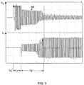
- Discharge lamps in particular high-pressure discharge lamps, are supplied with an alternating voltage with the nominal frequency at the start of operation (time t o ) in the prior art.
- This is shown schematically in FIG. 1, the lamp voltage U L (with 200 V / unit) being shown in the upper part of FIG. 1 and the lamp current I L (with 2A / unit) in the lower part of FIG. 1.
- a voltage U L with the nominal frequency is supplied to the lamp from the time (t o ) when it is switched on.
- ignition pulses in a time period T1.
- the firing pulses have an amplitude of 4 to 4.5 KV and a width of 1-2 microseconds, so that the firing pulses are not shown in FIG.
- FIG. 2 shows schematically the voltage and current supply according to the method according to the invention, the lamp voltage U L (with 200 V / unit) in the upper part of FIG. 2 and the lamp current I L (with 2A / unit) in the lower part of FIG. is shown.
- a direct voltage U 1 with an amplitude of typically 280 to 350 volts is applied to the discharge lamp. Ignition pulses are superimposed on this DC voltage U 1 until the lamp breaks through, ie ignites (time t1). The ignition pulses are not shown in FIG. 2 for the reasons that have been described in connection with FIG. 1. No lamp current flows in period T1.
- the period T1 lasts, for example, only 1 ms.
- Figure 3 shows the period T1 in an enlarged view
- the period T2 begins with the ignition.
- the discharge lamp is operated with a direct current I2 in a first direction.
- the voltage is typically 10 to 20 volts.
- the period T2 is typically 300-500 ms (in FIG. 2: approx. 350 ms).
- the direct current I2 is typically 1.5 times the nominal current, that is to say the current in the nominal operating state (following T4), in particular 1.5 to 2 times the nominal current.
- the period T3 begins after the period T2.
- the discharge lamp is operated with a direct current I3 in a second direction, which is opposite to the first direction.
- the voltage is also typically 10 to 20 volts.
- T3 is shorter than T2; in particular, the time period T3 is 100-200 ms (in FIG. 2: approx. 110 ms).
- the direct current I3 is also typically 1.5 times the nominal current, that is to say the current in the nominal operating state (following T4), in particular 1.5 to 2 times the nominal current.
- the discharge lamp impressed with an alternating current with the nominal frequency which continues to be at least 1.5 times the nominal current.
- the AC voltage is still typically 10 to 20 volts.
- the lamp voltage increases from 10 to 20 volts to its nominal value of e.g. 80 to 100 volts and the lamp current drops to the nominal value of e.g. 1.8 A in a 150 watt lamp.
- the period T4 which depends, among other things, on the ratio of the starting current to the nominal current (in the present case: factor 1.5 to 2), takes about 1 to 2 minutes.
- the second predefinable period T2 is selected so that the lamp electrode, which is anode during this period, is heated to the temperature (e.g. 2000 ° K) at which the thermal emission of electrons begins.
- the third predefinable period T3 is selected so that the lamp electrode, which is anode during this period T3 (in T2: cathode), is heated to the temperature (e.g. 2000 ° K) at which the thermal emission of electrons begins.
- the third predeterminable period T3 is shorter than the second predeterminable period T2.
- the lamp current can be higher during the second and / or third period T2, T3 than the lamp current subsequently formed in the period T4.
- the lamp current during the periods T2, T3 is at least 1.5 times higher than the lamp current subsequently formed.
- the circuit shown in FIG. 4 represents an example of a circuit arrangement for carrying out the method according to the invention, which forms part of an electronic ballast.
- This circuit arrangement is divided into the following blocks: power supply SV, full bridge VB, bridge driver BT, ignition Z, and control part C.
- the first four blocks SV, VB, BT and Z can be constructed identically to corresponding blocks in conventional circuit arrangements.
- the circuit arrangement has a control part which, for example, can be constructed like arrangement C shown in FIG.
- the control part C has a sensor S and timing elements ZG1, ZG2, ZG3 and ZG4, the sensor S being connected directly upstream of the timing element ZG2, which forms the period T2.
- the sensor S is used to detect the amount of the lamp voltage and consists of resistors R9, R10 and R11 and a capacitor C7.
- the lamp voltage tapped off via the voltage divider R9, R10, R11 is supplied to the timing element ZG2 via a diode D5, the circuit design and mode of operation of which are still to be described.
- the timing element ZG1 consists of a capacitor C6: an opposing stand R13, two diodes (in the block shown in dashed lines) D8 and a Schmitt trigger ST1. It is used to initialize the BT bridge driver, which works as follows:
- the capacitor C6 Before the operating voltage is switched on, the capacitor C6 is discharged (0 volt).
- the output of the Schmitt trigger ST1 is at 0 volts.
- a Schmitt trigger ST3 which is connected downstream of the timing element ZG1, and a Schmitt trigger ST4 (in the timing element ZG4) Bridge driver BT, the power transistors T2 and T4 of the full bridge VB.
- the Schmitt trigger ST1 switches from 0 volts to 15 volts at its output.
- the power transistor T2 is turned off and the power transistor T1 is turned on.
- the voltage at the input of the full bridge is switched through to the output of the full bridge VB.
- the ignition in the discharge lamp LP is thus released.
- the timing element ZG2 has a capacitor C8 and a resistor R14. After the lamp has been ignited (end of period T1 or beginning of period T2 in FIGS. 2 and 3), the voltage at the voltage divider of sensor S and at the anode of D5 drops, for example from 15 volts to 1 volt. The diode D5 blocks. The potential at the cathode of D5 drops from 15 volts after an e-function with the time constants of C8 and R14. If a Schmitt trigger ST2, which is arranged between the timing elements ZG2 and ZG3, falls below a threshold voltage, the latter switches from 0 volts to 15 volts at its output. The Schmitt trigger ST4 switches from 0 volts to 15 volts at its input and from 15 volts to 0 volts at its output.
- the downstream Schmitt trigger ST3 switches from 15 volts to 0 volts at its input and from 0 volts to 15 volts at its output.
- the full bridge VB is thus switched (transistors T1 and T4 from “ON” to “OFF”; and transistors T2 and T3 from “OFF” to “ON”) and the period T2 is ended.
- the period T2 is such that the one that functions as an anode during this period Electrode of the discharge lamp reaches its emission temperature. Typically, the T2 period is 500 milliseconds.
- the timer ZG3 is started. This consists of a capacitor C9, two diodes (in block D6 shown in dashed lines) and a resistor R16. Capacitor C9 charges to 15 volts via R16.
- the threshold voltage at the input of the Schmitt trigger ST4 is undershot, it switches from 0 volts to 15 volts at its output, while the Schmitt trigger ST3 switches from 15 volts to 0 volts at its output.
- the bridge VB is switched over again.
- the period T3 is thus ended. It is dimensioned such that the electrode of the discharge lamp LP, which acts as an anode during this period, reaches its emission temperature.
- the period T3 is typically shorter than the period T2 and is e.g. 200 ms.
- the nominal frequency is generated by this oscillator via the timing element ZG4, which has an oscillator C10, R16 and ST4.
- the discharge lamp LP is supplied with the alternating current at the nominal frequency.
- the signals of the oscillator ZG4 are fed to the full bridge VB with the help of the bridge driver BT and this switches the input voltage U E to the lamp at the nominal frequency.
- the nominal operating status of the lamp is then reached after about 1 - 2 minutes.
Landscapes
- Engineering & Computer Science (AREA)
- Power Engineering (AREA)
- Circuit Arrangements For Discharge Lamps (AREA)
Applications Claiming Priority (2)
| Application Number | Priority Date | Filing Date | Title |
|---|---|---|---|
| DE19509832A DE19509832A1 (de) | 1995-03-17 | 1995-03-17 | Verfahren und Schaltungsanordnung zum Betrieb einer Entladungslampe |
| DE19509832 | 1995-03-17 |
Publications (3)
| Publication Number | Publication Date |
|---|---|
| EP0732869A2 true EP0732869A2 (fr) | 1996-09-18 |
| EP0732869A3 EP0732869A3 (fr) | 1997-03-12 |
| EP0732869B1 EP0732869B1 (fr) | 2001-07-04 |
Family
ID=7757028
Family Applications (1)
| Application Number | Title | Priority Date | Filing Date |
|---|---|---|---|
| EP96103407A Expired - Lifetime EP0732869B1 (fr) | 1995-03-17 | 1996-03-05 | Procédé et circuit pour alimenter une lampe à décharge |
Country Status (4)
| Country | Link |
|---|---|
| US (1) | US5770924A (fr) |
| EP (1) | EP0732869B1 (fr) |
| CA (1) | CA2171931C (fr) |
| DE (2) | DE19509832A1 (fr) |
Families Citing this family (12)
| Publication number | Priority date | Publication date | Assignee | Title |
|---|---|---|---|---|
| US6172468B1 (en) * | 1997-01-14 | 2001-01-09 | Metrolight Ltd. | Method and apparatus for igniting a gas discharge lamp |
| JP3520795B2 (ja) * | 1999-02-15 | 2004-04-19 | 松下電工株式会社 | 放電灯点灯装置 |
| DE10126011A1 (de) * | 2001-05-28 | 2002-12-05 | Patent Treuhand Ges Fuer Elektrische Gluehlampen Mbh | Verfahren zum Start einer Entladungslampe |
| JP3893042B2 (ja) * | 2001-10-26 | 2007-03-14 | 松下電器産業株式会社 | 高圧放電ランプの点灯方法、点灯装置及び高圧放電ランプ装置 |
| DE10252979A1 (de) * | 2002-11-14 | 2004-06-03 | Diehl Luftfahrt Elektronik Gmbh | Verfahren zum Betreiben einer Gasentladungslampe und Vorschaltgerät |
| US7109668B2 (en) * | 2003-10-30 | 2006-09-19 | I.E.P.C. Corp. | Electronic lighting ballast |
| US20070194721A1 (en) * | 2004-08-20 | 2007-08-23 | Vatche Vorperian | Electronic lighting ballast with multiple outputs to drive electric discharge lamps of different wattage |
| US20060175973A1 (en) * | 2005-02-07 | 2006-08-10 | Lisitsyn Igor V | Xenon lamp |
| JP4820702B2 (ja) * | 2006-07-20 | 2011-11-24 | オスラム・メルコ株式会社 | 超高圧水銀ランプ |
| JP5112096B2 (ja) * | 2008-02-04 | 2013-01-09 | 株式会社小糸製作所 | 放電灯点灯回路 |
| JP5376409B2 (ja) * | 2010-01-07 | 2013-12-25 | ウシオ電機株式会社 | 光源装置および光照射装置 |
| DE102010031219A1 (de) * | 2010-07-12 | 2012-01-12 | Osram Gesellschaft mit beschränkter Haftung | Schaltungsanordnung und Verfahren zum Betreiben mindestens einer Entladungslampe |
Family Cites Families (6)
| Publication number | Priority date | Publication date | Assignee | Title |
|---|---|---|---|---|
| JPS59198699A (ja) * | 1983-04-27 | 1984-11-10 | 株式会社日立製作所 | 高圧放電灯の点灯方法 |
| US4709188A (en) * | 1985-12-23 | 1987-11-24 | General Electric Company | Operation of standby filament associated with an AC arc discharge lamp ballast |
| EP0411617A3 (en) * | 1989-08-01 | 1992-05-13 | Toshiba Lighting & Technology Corporation | Method of lighting discharge lamp and discharge lamp lighting apparatus |
| DE69113506T2 (de) * | 1990-05-10 | 1996-06-13 | Matsushita Electric Ind Co Ltd | Apparat zum Betreiben einer Entladungslampe. |
| DE4015398A1 (de) * | 1990-05-14 | 1991-11-21 | Hella Kg Hueck & Co | Verfahren und einrichtung zum starten einer hochdruckgasentladungslampe in kraftfahrzeugen |
| JP3447776B2 (ja) * | 1993-09-17 | 2003-09-16 | 池田デンソー株式会社 | 放電灯点灯装置 |
-
1995
- 1995-03-17 DE DE19509832A patent/DE19509832A1/de not_active Withdrawn
-
1996
- 1996-03-04 US US08/610,634 patent/US5770924A/en not_active Expired - Lifetime
- 1996-03-05 DE DE59607194T patent/DE59607194D1/de not_active Expired - Lifetime
- 1996-03-05 EP EP96103407A patent/EP0732869B1/fr not_active Expired - Lifetime
- 1996-03-15 CA CA002171931A patent/CA2171931C/fr not_active Expired - Fee Related
Also Published As
| Publication number | Publication date |
|---|---|
| US5770924A (en) | 1998-06-23 |
| CA2171931C (fr) | 2004-06-29 |
| EP0732869B1 (fr) | 2001-07-04 |
| EP0732869A3 (fr) | 1997-03-12 |
| DE19509832A1 (de) | 1996-09-19 |
| DE59607194D1 (de) | 2001-08-09 |
| CA2171931A1 (fr) | 1996-09-18 |
Similar Documents
| Publication | Publication Date | Title |
|---|---|---|
| DE4109325C2 (de) | Schaltungsanordnung zum Betrieb einer Hochdruck-Entladungslampe | |
| EP1103165B1 (fr) | Ballast electronique destine a au moins une lampe a decharge basse tension | |
| DE4331378C2 (de) | Schaltungsanordnung zum Betrieb einer Hochdruck-Entladungslampe für einen Fahrzeugscheinwerfer | |
| DE10006466B4 (de) | Vorschaltgerät für eine Hochdruck-Gasentladungslampe | |
| DE60205830T2 (de) | Vorschaltgerät mit effizienter Elektroden-Vorheizung und Lampenfehlerschutz | |
| EP2163139B1 (fr) | Arrangement de circuit et procédé pour faire fonctionner au moins une led et au moins un tube fluorescent | |
| DE4412518C2 (de) | Schaltungsanordnung zum Zünden und Betreiben einer Hochdruck-Entladungslampe | |
| DE10196562B4 (de) | Vorschaltgerät für den Betrieb einer Entladungslampe | |
| EP0740492B1 (fr) | Procédé et circuit pour amorcer et alimenter d'une lampe à décharge | |
| EP0732869B1 (fr) | Procédé et circuit pour alimenter une lampe à décharge | |
| DE68911342T2 (de) | Anlaufschaltungen für Entladungslampen. | |
| DE4309218A1 (de) | Niederspannungs-Vorschaltanordnung für eine Entladungs-Lichtquelle großer Helligkeit | |
| EP2000010B1 (fr) | Reglage de l'heure d'arret d'un onduleur pour le fonctionnement d'une lampe | |
| DE69911376T2 (de) | Verfahren und anordnung zum betreiben von elektronischen vorschaltgeräten für entladungslampen hoher intensität | |
| EP0868115B1 (fr) | Circuit d'amorçage pour lampe HID | |
| DE19626101A1 (de) | Beleuchtungsgerät mit Entladungslampe | |
| DE60122192T2 (de) | Schaltungsanordnung | |
| DE69616451T2 (de) | Umschaltanordnung | |
| EP0824849B1 (fr) | Dispositif pour detecter l'allumage d'une lampe luminescente a gaz a haute pression | |
| EP1086609B1 (fr) | Allumeur pour lampe luminescente a gaz, notamment lampe luminescente a gaz haute pression pour phare de vehicule automobile | |
| EP1476003B1 (fr) | Circuit d'alimentation et méthode pour l'alimentation de lampes à décharge gazeuse | |
| DE69817326T2 (de) | Vorschaltgerät | |
| EP1276355A2 (fr) | Circuit ballast pour determiner la puissance de préchauffage | |
| EP1771045B1 (fr) | Circuit d' amorçage pour une lampe à décharge haute-pression | |
| DE3208607C2 (fr) |
Legal Events
| Date | Code | Title | Description |
|---|---|---|---|
| PUAI | Public reference made under article 153(3) epc to a published international application that has entered the european phase |
Free format text: ORIGINAL CODE: 0009012 |
|
| AK | Designated contracting states |
Kind code of ref document: A2 Designated state(s): BE DE FR GB IT NL |
|
| PUAL | Search report despatched |
Free format text: ORIGINAL CODE: 0009013 |
|
| AK | Designated contracting states |
Kind code of ref document: A3 Designated state(s): BE DE FR GB IT NL |
|
| 17P | Request for examination filed |
Effective date: 19970404 |
|
| GRAG | Despatch of communication of intention to grant |
Free format text: ORIGINAL CODE: EPIDOS AGRA |
|
| 17Q | First examination report despatched |
Effective date: 20000914 |
|
| GRAG | Despatch of communication of intention to grant |
Free format text: ORIGINAL CODE: EPIDOS AGRA |
|
| GRAH | Despatch of communication of intention to grant a patent |
Free format text: ORIGINAL CODE: EPIDOS IGRA |
|
| RIC1 | Information provided on ipc code assigned before grant |
Free format text: 7H 05B 41/295 A, 7H 05B 41/38 B |
|
| GRAH | Despatch of communication of intention to grant a patent |
Free format text: ORIGINAL CODE: EPIDOS IGRA |
|
| GRAA | (expected) grant |
Free format text: ORIGINAL CODE: 0009210 |
|
| AK | Designated contracting states |
Kind code of ref document: B1 Designated state(s): BE DE FR GB IT NL |
|
| REF | Corresponds to: |
Ref document number: 59607194 Country of ref document: DE Date of ref document: 20010809 |
|
| ITF | It: translation for a ep patent filed | ||
| GBT | Gb: translation of ep patent filed (gb section 77(6)(a)/1977) |
Effective date: 20010920 |
|
| ET | Fr: translation filed | ||
| REG | Reference to a national code |
Ref country code: GB Ref legal event code: IF02 |
|
| PLBE | No opposition filed within time limit |
Free format text: ORIGINAL CODE: 0009261 |
|
| STAA | Information on the status of an ep patent application or granted ep patent |
Free format text: STATUS: NO OPPOSITION FILED WITHIN TIME LIMIT |
|
| 26N | No opposition filed | ||
| PGFP | Annual fee paid to national office [announced via postgrant information from national office to epo] |
Ref country code: NL Payment date: 20110315 Year of fee payment: 16 |
|
| PGFP | Annual fee paid to national office [announced via postgrant information from national office to epo] |
Ref country code: IT Payment date: 20110330 Year of fee payment: 16 |
|
| REG | Reference to a national code |
Ref country code: DE Ref legal event code: R081 Ref document number: 59607194 Country of ref document: DE Owner name: OSRAM GMBH, DE Free format text: FORMER OWNER: OSRAM GESELLSCHAFT MIT BESCHRAENKTER HAFTUNG, 81543 MUENCHEN, DE Effective date: 20111130 |
|
| PG25 | Lapsed in a contracting state [announced via postgrant information from national office to epo] |
Ref country code: DE Free format text: LAPSE BECAUSE OF NON-PAYMENT OF DUE FEES Effective date: 20111001 |
|
| REG | Reference to a national code |
Ref country code: NL Ref legal event code: V1 Effective date: 20121001 |
|
| PG25 | Lapsed in a contracting state [announced via postgrant information from national office to epo] |
Ref country code: IT Free format text: LAPSE BECAUSE OF NON-PAYMENT OF DUE FEES Effective date: 20120305 |
|
| REG | Reference to a national code |
Ref country code: DE Ref legal event code: R081 Ref document number: 59607194 Country of ref document: DE Owner name: OSRAM GMBH, DE Free format text: FORMER OWNER: OSRAM AG, 81543 MUENCHEN, DE Effective date: 20130205 |
|
| PG25 | Lapsed in a contracting state [announced via postgrant information from national office to epo] |
Ref country code: NL Free format text: LAPSE BECAUSE OF NON-PAYMENT OF DUE FEES Effective date: 20121001 |
|
| REG | Reference to a national code |
Ref country code: DE Ref legal event code: R081 Ref document number: 59607194 Country of ref document: DE Owner name: OSRAM GMBH, DE Free format text: FORMER OWNER: OSRAM GMBH, 81543 MUENCHEN, DE Effective date: 20130822 |
|
| PGFP | Annual fee paid to national office [announced via postgrant information from national office to epo] |
Ref country code: FR Payment date: 20140319 Year of fee payment: 19 |
|
| PGFP | Annual fee paid to national office [announced via postgrant information from national office to epo] |
Ref country code: GB Payment date: 20140319 Year of fee payment: 19 |
|
| PGFP | Annual fee paid to national office [announced via postgrant information from national office to epo] |
Ref country code: BE Payment date: 20140319 Year of fee payment: 19 |
|
| PGFP | Annual fee paid to national office [announced via postgrant information from national office to epo] |
Ref country code: DE Payment date: 20150320 Year of fee payment: 20 |
|
| GBPC | Gb: european patent ceased through non-payment of renewal fee |
Effective date: 20150305 |
|
| REG | Reference to a national code |
Ref country code: FR Ref legal event code: ST Effective date: 20151130 |
|
| PG25 | Lapsed in a contracting state [announced via postgrant information from national office to epo] |
Ref country code: GB Free format text: LAPSE BECAUSE OF NON-PAYMENT OF DUE FEES Effective date: 20150305 |
|
| PG25 | Lapsed in a contracting state [announced via postgrant information from national office to epo] |
Ref country code: FR Free format text: LAPSE BECAUSE OF NON-PAYMENT OF DUE FEES Effective date: 20150331 |
|
| REG | Reference to a national code |
Ref country code: DE Ref legal event code: R071 Ref document number: 59607194 Country of ref document: DE |
|
| PG25 | Lapsed in a contracting state [announced via postgrant information from national office to epo] |
Ref country code: BE Free format text: LAPSE BECAUSE OF NON-PAYMENT OF DUE FEES Effective date: 20150331 |