EP0733281B1 - Dispositif amplificateur - Google Patents
Dispositif amplificateur Download PDFInfo
- Publication number
- EP0733281B1 EP0733281B1 EP95929991A EP95929991A EP0733281B1 EP 0733281 B1 EP0733281 B1 EP 0733281B1 EP 95929991 A EP95929991 A EP 95929991A EP 95929991 A EP95929991 A EP 95929991A EP 0733281 B1 EP0733281 B1 EP 0733281B1
- Authority
- EP
- European Patent Office
- Prior art keywords
- transistor
- coupled
- current
- main electrode
- transistors
- Prior art date
- Legal status (The legal status is an assumption and is not a legal conclusion. Google has not performed a legal analysis and makes no representation as to the accuracy of the status listed.)
- Expired - Lifetime
Links
- 238000010586 diagram Methods 0.000 description 10
- 230000007423 decrease Effects 0.000 description 7
- 230000008878 coupling Effects 0.000 description 2
- 238000010168 coupling process Methods 0.000 description 2
- 238000005859 coupling reaction Methods 0.000 description 2
- 230000000694 effects Effects 0.000 description 2
- 230000003321 amplification Effects 0.000 description 1
- 230000001419 dependent effect Effects 0.000 description 1
- 238000003199 nucleic acid amplification method Methods 0.000 description 1
- 230000003071 parasitic effect Effects 0.000 description 1
- 238000009877 rendering Methods 0.000 description 1
Images


Classifications
-
- H—ELECTRICITY
- H03—ELECTRONIC CIRCUITRY
- H03F—AMPLIFIERS
- H03F1/00—Details of amplifiers with only discharge tubes, only semiconductor devices or only unspecified devices as amplifying elements
- H03F1/32—Modifications of amplifiers to reduce non-linear distortion
- H03F1/3217—Modifications of amplifiers to reduce non-linear distortion in single ended push-pull amplifiers
-
- H—ELECTRICITY
- H03—ELECTRONIC CIRCUITRY
- H03F—AMPLIFIERS
- H03F3/00—Amplifiers with only discharge tubes or only semiconductor devices as amplifying elements
- H03F3/30—Single-ended push-pull [SEPP] amplifiers; Phase-splitters therefor
Definitions
- the invention relates to an amplifier arrangement as defined in the preamble of claim 1.
- Such an amplifier arrangement is known from the United States patent US-A-5,057,790.
- an audio amplifier is described which reduces crossover distortion typical of class AB push-pull amplifiers by including means for preventing either of the output transistors from being cut off during any portion of the audio waveform.
- the circuit includes two base-emitter voltage multipliers and a non-linear transconductance feedback amplifier.
- the driver stage in the known amplifier arrangement comprises third and fourth transistors coupled anti-parallel between the first and second outputs of the driver stage.
- the control electrodes of third and fourth transistors are coupled to respective biasing means.
- the input of the driver stage is coupled to the second output of the driver stage, so that a signal current applied to the input is directly applied to the control electrode of the second transistor.
- a signal current applied to the input terminal will result in a simultaneous increase or decrease of the potentials on the control electrodes of the first and second output transistors.
- An object of the invention is to provide an amplifier arrangement having a further reduced distortion.
- An amplifier arrangement comprises the features of claim 1.
- the invention is based on the recognition that distortion can be reduced by preventing the output transistors being turned off due to large input signals.
- the first current supplied by the first current source will be divided equally over the transistor couple, formed by the third and the fifth transistors, just as the second current supplied by the second current source will be divided equally over the transistor couple formed by the fourth and sixth transistors.
- a signal applied to the input of the driver stage will result in a different current division for each of the transistor couples. In the extreme situation one of the transistors in the couples can become current-less. If the third or fourth transistor becomes current-less the presence of the fifth or sixth transistor respectively will ensure that the first or second transistor remains biased, thus always conducting a minimum current.
- the output transistors cannot become non-conductive and consequently distortion is reduced.
- Figure 1 is a circuit diagram of a known amplifier arrangement using MOS transistors.
- the known amplifier arrangement comprises:
- FIG. 2 is a circuit diagram of a first embodiment of an amplifier arrangement according to the invention using MOS transistors.
- the driver stage 100 of figure 2 differs from the driver stage 100 of Figure 1 in the following:
- FIG 2 the drains of the transistors T5 and T6 are coupled to the second and first supply terminals 4 and 3, respectively.
- a signal current flowing through transistor T3 will see a low impedance at the gate of the first transistor T1, said low impedance being the impedance seen at the source of the fifth transistor T5.
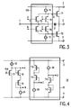
- Figure 3 is a circuit diagram of a second embodiment of an amplifier arrangement according to the invention using MOS transistors.
- the drains of the transistors T5 and T6 are both coupled to the input 5 of the driver stage 100. Through this feedback a very high impedance is realised at input 5.
- Figure 4 is a circuit diagram of an example of the biasing means for use in conjunction with the shown embodiments of the amplifier arrangement according to the invention.
- the biasing means 14 comprises:
- FIG. 5 is a circuit diagram of a further example of part 15 of the biasing means for use in conjunction with the shown embodiments of the amplifier arrangement according to the invention.
- This part 15 is biasing the gates of transistors T5 and T6.
- transistors T10, T11, T12 and T13 together with current sources 26 and 28 are replaced by the following:
- the invention is not limited to the embodiments using MOS transistors. It is also possible to use bipolar transistors, in which case gate, drain and source should be replaced by base, collector and emitter. A transistor of the first conductivity type will then be a PNP transistor and a transistor of the second conductivity type will be an NPN transistor. The source followers T5 and T6 should then be renamed emitter followers.
Landscapes
- Engineering & Computer Science (AREA)
- Power Engineering (AREA)
- Physics & Mathematics (AREA)
- Nonlinear Science (AREA)
- Amplifiers (AREA)
Claims (8)
- Dispositif amplificateur comprenant :lequel étage d'excitation (100) comprend :une borne d'entrée (1), une borne de sortie (2), une première (3) et une deuxième (4) bornes d'alimentation pour recevoir une tension d'alimentation ;un premier transistor (T1) d'un premier type de conductivité et un deuxième transistor (T2) d'un deuxième type de conductivité, comportant chacun une électrode de commande et une première et une deuxième électrodes principales ;un étage d'excitation (100), comportant une entrée (5) couplée à la borne d'entrée (1) et comportant une première (6) et une deuxième (7) sorties respectivement couplées aux électrodes de commande du premier (T1) et du deuxième (T2) transistors T1, T2 ;les deuxièmes électrodes principales du premier et du deuxième transistors (T1, T2) étant respectivement couplées à la première et à la deuxième bornes d'alimentation (3, 4), et les premières électrodes principales du premier et du deuxième transistors (T1, T2) étant couplées à la borne de sortie (2),caractérisé en ce que le premier transistor (T1) est un transistor du même premier type de conductivité que le quatrième et le cinquième transistors (T4, T5) tandis que le deuxième transistor (T2) est un transistor du même deuxième type de conductivité que le troisième et le sixième transistors (T3, T6), et en ce que le moyen de polarisation (14) comprend :des troisième et sixième transistors (T3, T6) et des quatrième et cinquième transistors (T4, T5), chaque transistor comportant une électrode de commande, une première et une deuxième électrodes principales ;une première source de courant (10) pour fournir un premier courant, couplée entre la première borne d'alimentation (1) et la première sortie (6) de l'étage d'excitation (100) ;une deuxième source de courant (12) pour fournir un deuxième courant, couplée entre la deuxième sortie (7) de l'étage d'excitation (100) et la deuxième borne d'alimentation (4) ;un moyen de polarisation (14) pour fournir des tensions de polarisation respectives aux électrodes de commande des troisième, quatrième, cinquième et sixième transistors (T3, T4, T5, T6) ;les deuxièmes électrodes principales du troisième et du quatrième transistors (T3, T4) étant couplées à l'entrée (5) de l'étage d'excitation (100) ;la première électrode principale du troisième transistor (T3) et la deuxième électrode principale du cinquième transistor (T5) étant couplées à la première sortie (6) de l'étage d'excitation (100) ;la première électrode principale du quatrième transistor (T4) et la deuxième électrode principale du sixième transistor (T6) étant couplées à la deuxième sortie (7) de l'étage d'excitation (100),un septième, un huitième et un neuvième transistors (T7, T8, T9), comportant chacun une électrode de commande et une première et une deuxième électrodes principales, le huitième transistor (T8) étant du deuxième type de conductivité et le septième et le neuvième transistors (T7, T9) étant du premier type de conductivité ;une troisième source de courant (22) pour fournir un troisième courant étant couplée entre la première borne d'alimentation (3) et la deuxième électrode principale du septième transistor (T7) ;une quatrième source de courant (24) pour fournir un quatrième courant, couplée entre la première électrode principale du neuvième transistor (T9) et la deuxième borne d'alimentation (4) ;l'électrode de commande et la première électrode principale du huitième transistor (T8) étant couplées à la deuxième électrode principale du septième transistor (T7) ;les deuxièmes électrodes principales des huitième et neuvième transistors (T8, T9) étant reliées entre elles ;la première électrode principale du neuvième transistor (T9) étant couplée à l'électrode de commande dudit transistor (T9) ;l'électrode de commande du septième transistor (T7) étant couplée à une tension de référence, etles électrodes de commande des huitième et neuvième transistors (T8, T9) étant respectivement couplées aux électrodes de commande du troisième et du quatrième transistors (T3, T4).
- Dispositif amplificateur suivant la revendication 1, caractérisé en ce que les premières électrodes principales du cinquième et du sixième transistors (T5, T6) sont couplées à l'entrée (5) de l'étage d'excitation (100).
- Dispositif amplificateur suivant la revendication 2, caractérisé en ce que le dispositif amplificateur comprend une capacité (21) couplée entre la borne de sortie (2) et l'entrée (5) de l'étage d'excitation (100).
- Dispositif amplificateur suivant la revendication 1, caractérisé en ce que la valeur du quatrième courant est pratiquement égale à la moitié de la valeur du premier courant, et en ce que la valeur du premier courant est pratiquement égale à la valeur du deuxième courant.
- Dispositif amplificateur suivant la revendication 1 ou 4, caractérisé en ce que le moyen de polarisation (14) comprend en outre :une cinquième source de courant (26) pour fournir un cinquième courant et un dixième et un onzième transistors (T10, T11), chaque transistor étant du premier type de conductivité et comportant une électrode de commande et une première et une deuxième électrodes principales ;la cinquième source de courant (26) étant couplée entre la deuxième borne d'alimentation (4) et la première électrode principale du onzième transistor (T11), l'électrode de commande et la première électrode principale du onzième transistor (T11) étant reliées entre elles, la deuxième électrode principale du onzième transistor (T11) étant couplée à l'électrode de commande et la première électrode principale du dixième transistor (T10), la deuxième électrode principale du dixième transistor (T10) étant couplée à la première borne d'alimentation (3) ;une sixième source de courant (28) pour fournir un sixième courant et un douzième et un treizième transistors (T12, T13), chaque transistor étant du deuxième type de conductivité et comportant une électrode de commande et une première et une deuxième électrodes principales, la sixième source de courant (28) étant couplée entre la première borne d'alimentation (3) et la première électrode principale du douzième transistor (T12), l'électrode de commande et la première électrode principale du douzième transistor (T12) étant reliées entre elles, la deuxième électrode principale du douzième transistor (T12) étant couplée à l'électrode de commande et à la première électrode principale du treizième transistor (T13), la deuxième électrode principale du treizième transistor (T13) étant couplée à la deuxième borne d'alimentation (4).
- Dispositif amplificateur suivant la revendication 5, caractérisé en ce que les valeurs du cinquième et du sixième courants sont chacune pratiquement égales à la moitié de la valeur du premier courant.
- Dispositif amplificateur suivant la revendication 1 ou 4, caractérisé en ce que le moyen de polarisation (14) comprend en outre :un dixième, un onzième, un douzième, un treizième, un quatorzième et un quinzième transistors (T14, T15, T16, T17, T18, T19), comportant chacun une électrode de commande, une première et une deuxième électrodes principales, le dixième, le quatorzième et le quinzième transistors (T14, T18, T19) étant du premier type de conductivité et le onzième, le douzième et le treizième transistors (T15, T16, T17) étant du deuxième type de conductivité ;une cinquième source de courant (30) pour fournir un cinquième courant, couplée entre la première borne d'alimentation (3) et la deuxième électrode principale du dixième transistor (T14) ;l'électrode de commande du dixième transistor (T14) étant couplée à l'électrode de commande du quatrième transistor (T4) et la première électrode principale du dixième transistor (T14) étant couplée à l'électrode de commande et à la première électrode principale du onzième transistor (T15) et à l'électrode de commande du sixième transistor (T6) ;une sixième source de courant (32) pour fournir un sixième courant, couplée entre la deuxième électrode principale du onzième transistor (T15) et la deuxième borne d'alimentation (4) ;la première électrode principale du douzième transistor (T16) étant couplée à la deuxième électrode principale du dixième transistor (T14) ;la deuxième électrode principale du douzième transistor (T16) étant couplée à la deuxième borne d'alimentation (4) ;l'électrode de commande du douzième transistor (T16) étant couplée à la deuxième électrode principale du onzième transistor (T15);une septième source de courant (34) pour fournir un septième courant, couplée entre la deuxième borne d'alimentation (3) et la deuxième électrode principale du quatorzième transistor (T18) ;une huitième source de courant (36) pour fournir un huitième courant, couplée entre la deuxième borne d'alimentation (4) et la deuxième électrode principale du treizième transistor (T17) ;l'électrode de commande du treizième transistor (T17) étant couplée à l'électrode de commande du troisième transistor (T3) et la première électrode principale du treizième transistor (T17) étant couplée à l'électrode de commande et à la première électrode principale du quatorzième transistor (T18) et à l'électrode de commande du cinquième transistor (T5) ;la première électrode principale du quinzième transistor (T19) étant couplée à la deuxième électrode principale du treizième transistor (T17) ;la deuxième électrode principale du quinzième transistor (T19) étant couplée à la première borne d'alimentation (3), etl'électrode de commande du quinzième transistor (T19) étant couplée à la deuxième électrode principale du quatorzième transistor (T18).
- Dispositif amplificateur suivant la revendication 7, caractérisé en ce que les valeurs du sixième et du huitième courants sont chacune pratiquement égales à la moitié de la valeur du premier courant.
Applications Claiming Priority (3)
| Application Number | Priority Date | Filing Date | Title |
|---|---|---|---|
| EP94202924 | 1994-10-10 | ||
| NL9420292 | 1994-10-10 | ||
| PCT/IB1995/000774 WO1996011528A2 (fr) | 1994-10-10 | 1995-09-21 | Dispositif amplificateur |
Publications (2)
| Publication Number | Publication Date |
|---|---|
| EP0733281A1 EP0733281A1 (fr) | 1996-09-25 |
| EP0733281B1 true EP0733281B1 (fr) | 2001-06-13 |
Family
ID=8217266
Family Applications (1)
| Application Number | Title | Priority Date | Filing Date |
|---|---|---|---|
| EP95929991A Expired - Lifetime EP0733281B1 (fr) | 1994-10-10 | 1995-09-21 | Dispositif amplificateur |
Country Status (5)
| Country | Link |
|---|---|
| US (1) | US5955923A (fr) |
| EP (1) | EP0733281B1 (fr) |
| KR (1) | KR960706713A (fr) |
| TW (1) | TW298685B (fr) |
| WO (1) | WO1996011528A2 (fr) |
Families Citing this family (3)
| Publication number | Priority date | Publication date | Assignee | Title |
|---|---|---|---|---|
| WO2002013374A1 (fr) | 2000-08-07 | 2002-02-14 | Koninklijke Philips Electronics N.V. | Amplificateur a impedances d'entree et de bruit adaptees |
| US6765438B1 (en) | 2001-11-01 | 2004-07-20 | Bae Systems Information And Electronic Systems Integration, Inc. | Transconductance power amplifier |
| JP4822144B2 (ja) * | 2006-03-17 | 2011-11-24 | エスティー‐エリクソン、ソシエテ、アノニム | リップル補償を備える供給回路 |
Family Cites Families (5)
| Publication number | Priority date | Publication date | Assignee | Title |
|---|---|---|---|---|
| US4570128A (en) * | 1984-07-05 | 1986-02-11 | National Semiconductor Corporation | Class AB output circuit with large swing |
| US4857863A (en) * | 1988-08-25 | 1989-08-15 | Motorola, Inc. | Low power output driver circuit with slew rate limiting |
| US5039953A (en) * | 1990-05-18 | 1991-08-13 | Hewlett-Packard Company | Class AB CMOS output amplifier |
| US5057790A (en) * | 1990-07-16 | 1991-10-15 | Landi Ernest D | High efficiency class A amplifier |
| US5218321A (en) * | 1991-06-18 | 1993-06-08 | Harris Corporation | Low offset unity gain buffer amplifier |
-
1995
- 1995-09-21 KR KR1019960703029A patent/KR960706713A/ko not_active Abandoned
- 1995-09-21 WO PCT/IB1995/000774 patent/WO1996011528A2/fr not_active Ceased
- 1995-09-21 EP EP95929991A patent/EP0733281B1/fr not_active Expired - Lifetime
- 1995-09-27 TW TW084110136A patent/TW298685B/zh active
- 1995-10-03 US US08/538,510 patent/US5955923A/en not_active Expired - Fee Related
Also Published As
| Publication number | Publication date |
|---|---|
| KR960706713A (ko) | 1996-12-09 |
| TW298685B (fr) | 1997-02-21 |
| WO1996011528A2 (fr) | 1996-04-18 |
| WO1996011528A3 (fr) | 1996-07-25 |
| EP0733281A1 (fr) | 1996-09-25 |
| US5955923A (en) | 1999-09-21 |
Similar Documents
| Publication | Publication Date | Title |
|---|---|---|
| US5343164A (en) | Operational amplifier circuit with slew rate enhancement | |
| US6437645B1 (en) | Slew rate boost circuitry and method | |
| US8797100B2 (en) | Circuit unit, bias circuit with circuit unit and differential amplifier circuit with first and second circuit unit | |
| US20040066234A1 (en) | Capacitor coupled dynamic bias boosting circuit for a power amplifier | |
| US6359516B1 (en) | High-frequency amplifier circuit with independent control of quiescent current and bias impedance | |
| EP0488315B1 (fr) | Un miroir de courant en cascode symétrique | |
| US6417734B1 (en) | High-frequency amplifier circuit with negative impedance cancellation | |
| US4336503A (en) | Driver circuit having reduced cross-over distortion | |
| EP0522786B1 (fr) | Amplification du type classe A avec polarisation glissante | |
| JPH0213487B2 (fr) | ||
| US4451800A (en) | Input bias adjustment circuit for amplifier | |
| US4801893A (en) | Forward transimpedance amplifier | |
| EP0733281B1 (fr) | Dispositif amplificateur | |
| KR987001154A (ko) | 증폭기 | |
| JPS60257610A (ja) | 能動負荷回路 | |
| KR930007295B1 (ko) | 증폭기 장치 | |
| US4165494A (en) | Bi-state linear amplifier | |
| US4492929A (en) | Operational amplifier having enhanced gain through current feedback | |
| CA1236889A (fr) | Amplificateur | |
| EP0703661A2 (fr) | Circuit de polarisation à source de tension unique pour un transistor à effet de champ | |
| JPS6096005A (ja) | ダイエリアを効率的に用いたノイズのないカスコード回路 | |
| US4420726A (en) | Voltage-followers with low offset voltages | |
| US7012465B2 (en) | Low-voltage class-AB output stage amplifier | |
| US20020140509A1 (en) | Efficient AC coupled CMOS RF amplifier | |
| US4409561A (en) | Operational amplifier output stage driven by a single ended gain stage |
Legal Events
| Date | Code | Title | Description |
|---|---|---|---|
| PUAI | Public reference made under article 153(3) epc to a published international application that has entered the european phase |
Free format text: ORIGINAL CODE: 0009012 |
|
| AK | Designated contracting states |
Kind code of ref document: A1 Designated state(s): DE FR GB IT |
|
| D17D | Deferred search report published (deleted) | ||
| 17P | Request for examination filed |
Effective date: 19961018 |
|
| 17Q | First examination report despatched |
Effective date: 19991111 |
|
| GRAG | Despatch of communication of intention to grant |
Free format text: ORIGINAL CODE: EPIDOS AGRA |
|
| GRAG | Despatch of communication of intention to grant |
Free format text: ORIGINAL CODE: EPIDOS AGRA |
|
| GRAH | Despatch of communication of intention to grant a patent |
Free format text: ORIGINAL CODE: EPIDOS IGRA |
|
| GRAH | Despatch of communication of intention to grant a patent |
Free format text: ORIGINAL CODE: EPIDOS IGRA |
|
| GRAA | (expected) grant |
Free format text: ORIGINAL CODE: 0009210 |
|
| AK | Designated contracting states |
Kind code of ref document: B1 Designated state(s): DE FR GB IT |
|
| PG25 | Lapsed in a contracting state [announced via postgrant information from national office to epo] |
Ref country code: IT Free format text: LAPSE BECAUSE OF FAILURE TO SUBMIT A TRANSLATION OF THE DESCRIPTION OR TO PAY THE FEE WITHIN THE PRE;WARNING: LAPSES OF ITALIAN PATENTS WITH EFFECTIVE DATE BEFORE 2007 MAY HAVE OCCURRED AT ANY TIME BEFORE 2007. THE CORRECT EFFECTIVE DATE MAY BE DIFFERENT FROM THE ONE RECORDED.SCRIBED TIME-LIMIT Effective date: 20010613 |
|
| REF | Corresponds to: |
Ref document number: 69521286 Country of ref document: DE Date of ref document: 20010719 |
|
| PGFP | Annual fee paid to national office [announced via postgrant information from national office to epo] |
Ref country code: FR Payment date: 20010925 Year of fee payment: 7 |
|
| ET | Fr: translation filed | ||
| PGFP | Annual fee paid to national office [announced via postgrant information from national office to epo] |
Ref country code: GB Payment date: 20011001 Year of fee payment: 7 |
|
| PGFP | Annual fee paid to national office [announced via postgrant information from national office to epo] |
Ref country code: DE Payment date: 20011121 Year of fee payment: 7 |
|
| REG | Reference to a national code |
Ref country code: GB Ref legal event code: IF02 |
|
| PLBE | No opposition filed within time limit |
Free format text: ORIGINAL CODE: 0009261 |
|
| STAA | Information on the status of an ep patent application or granted ep patent |
Free format text: STATUS: NO OPPOSITION FILED WITHIN TIME LIMIT |
|
| 26N | No opposition filed | ||
| PG25 | Lapsed in a contracting state [announced via postgrant information from national office to epo] |
Ref country code: GB Free format text: LAPSE BECAUSE OF NON-PAYMENT OF DUE FEES Effective date: 20020921 |
|
| PG25 | Lapsed in a contracting state [announced via postgrant information from national office to epo] |
Ref country code: DE Free format text: LAPSE BECAUSE OF NON-PAYMENT OF DUE FEES Effective date: 20030401 |
|
| GBPC | Gb: european patent ceased through non-payment of renewal fee |
Effective date: 20020921 |
|
| PG25 | Lapsed in a contracting state [announced via postgrant information from national office to epo] |
Ref country code: FR Free format text: LAPSE BECAUSE OF NON-PAYMENT OF DUE FEES Effective date: 20030603 |
|
| REG | Reference to a national code |
Ref country code: FR Ref legal event code: ST |