EP0733888A1 - Dispositif de mesure - Google Patents
Dispositif de mesure Download PDFInfo
- Publication number
- EP0733888A1 EP0733888A1 EP96301378A EP96301378A EP0733888A1 EP 0733888 A1 EP0733888 A1 EP 0733888A1 EP 96301378 A EP96301378 A EP 96301378A EP 96301378 A EP96301378 A EP 96301378A EP 0733888 A1 EP0733888 A1 EP 0733888A1
- Authority
- EP
- European Patent Office
- Prior art keywords
- interferometer
- optical path
- path length
- light
- signal
- Prior art date
- Legal status (The legal status is an assumption and is not a legal conclusion. Google has not performed a legal analysis and makes no representation as to the accuracy of the status listed.)
- Granted
Links
- 230000003287 optical effect Effects 0.000 claims description 63
- 230000005855 radiation Effects 0.000 claims description 14
- 238000012545 processing Methods 0.000 claims description 8
- 230000010355 oscillation Effects 0.000 claims description 3
- 230000001427 coherent effect Effects 0.000 abstract description 13
- 239000013307 optical fiber Substances 0.000 description 21
- 239000000463 material Substances 0.000 description 17
- 230000008859 change Effects 0.000 description 15
- 238000005259 measurement Methods 0.000 description 13
- 230000035945 sensitivity Effects 0.000 description 8
- 238000012937 correction Methods 0.000 description 7
- 239000000758 substrate Substances 0.000 description 7
- 238000005562 fading Methods 0.000 description 6
- XUIMIQQOPSSXEZ-UHFFFAOYSA-N Silicon Chemical compound [Si] XUIMIQQOPSSXEZ-UHFFFAOYSA-N 0.000 description 5
- 238000010586 diagram Methods 0.000 description 5
- 229910052710 silicon Inorganic materials 0.000 description 5
- 239000010703 silicon Substances 0.000 description 5
- VYPSYNLAJGMNEJ-UHFFFAOYSA-N Silicium dioxide Chemical compound O=[Si]=O VYPSYNLAJGMNEJ-UHFFFAOYSA-N 0.000 description 4
- XLOMVQKBTHCTTD-UHFFFAOYSA-N Zinc monoxide Chemical compound [Zn]=O XLOMVQKBTHCTTD-UHFFFAOYSA-N 0.000 description 4
- 238000001514 detection method Methods 0.000 description 4
- 230000004044 response Effects 0.000 description 4
- 230000035882 stress Effects 0.000 description 4
- 230000000694 effects Effects 0.000 description 3
- 239000000835 fiber Substances 0.000 description 3
- 238000000034 method Methods 0.000 description 3
- 239000004065 semiconductor Substances 0.000 description 3
- 238000005253 cladding Methods 0.000 description 2
- NKZSPGSOXYXWQA-UHFFFAOYSA-N dioxido(oxo)titanium;lead(2+) Chemical compound [Pb+2].[O-][Ti]([O-])=O NKZSPGSOXYXWQA-UHFFFAOYSA-N 0.000 description 2
- 230000005684 electric field Effects 0.000 description 2
- 239000002305 electric material Substances 0.000 description 2
- HFGPZNIAWCZYJU-UHFFFAOYSA-N lead zirconate titanate Chemical compound [O-2].[O-2].[O-2].[O-2].[O-2].[Ti+4].[Zr+4].[Pb+2] HFGPZNIAWCZYJU-UHFFFAOYSA-N 0.000 description 2
- 238000002310 reflectometry Methods 0.000 description 2
- 239000000377 silicon dioxide Substances 0.000 description 2
- 239000011787 zinc oxide Substances 0.000 description 2
- JBRZTFJDHDCESZ-UHFFFAOYSA-N AsGa Chemical compound [As]#[Ga] JBRZTFJDHDCESZ-UHFFFAOYSA-N 0.000 description 1
- 229910001218 Gallium arsenide Inorganic materials 0.000 description 1
- GPXJNWSHGFTCBW-UHFFFAOYSA-N Indium phosphide Chemical compound [In]#P GPXJNWSHGFTCBW-UHFFFAOYSA-N 0.000 description 1
- 229910052770 Uranium Inorganic materials 0.000 description 1
- 230000009471 action Effects 0.000 description 1
- 238000004458 analytical method Methods 0.000 description 1
- 238000004364 calculation method Methods 0.000 description 1
- 238000006243 chemical reaction Methods 0.000 description 1
- 238000005229 chemical vapour deposition Methods 0.000 description 1
- 230000001143 conditioned effect Effects 0.000 description 1
- 238000000151 deposition Methods 0.000 description 1
- 230000008021 deposition Effects 0.000 description 1
- 238000005516 engineering process Methods 0.000 description 1
- 238000001914 filtration Methods 0.000 description 1
- 238000010438 heat treatment Methods 0.000 description 1
- 230000007062 hydrolysis Effects 0.000 description 1
- 238000006460 hydrolysis reaction Methods 0.000 description 1
- 239000011810 insulating material Substances 0.000 description 1
- 230000010354 integration Effects 0.000 description 1
- 230000002452 interceptive effect Effects 0.000 description 1
- GQYHUHYESMUTHG-UHFFFAOYSA-N lithium niobate Chemical compound [Li+].[O-][Nb](=O)=O GQYHUHYESMUTHG-UHFFFAOYSA-N 0.000 description 1
- 238000004519 manufacturing process Methods 0.000 description 1
- 238000012986 modification Methods 0.000 description 1
- 230000004048 modification Effects 0.000 description 1
- 239000000382 optic material Substances 0.000 description 1
- 230000010363 phase shift Effects 0.000 description 1
- 239000007787 solid Substances 0.000 description 1
- 230000003595 spectral effect Effects 0.000 description 1
- 238000001228 spectrum Methods 0.000 description 1
- 230000008646 thermal stress Effects 0.000 description 1
- XOLBLPGZBRYERU-UHFFFAOYSA-N tin dioxide Chemical compound O=[Sn]=O XOLBLPGZBRYERU-UHFFFAOYSA-N 0.000 description 1
- 229910001887 tin oxide Inorganic materials 0.000 description 1
- 238000013519 translation Methods 0.000 description 1
- 239000012780 transparent material Substances 0.000 description 1
- 229910052720 vanadium Inorganic materials 0.000 description 1
Images


Classifications
-
- G—PHYSICS
- G01—MEASURING; TESTING
- G01L—MEASURING FORCE, STRESS, TORQUE, WORK, MECHANICAL POWER, MECHANICAL EFFICIENCY, OR FLUID PRESSURE
- G01L9/00—Measuring steady of quasi-steady pressure of fluid or fluent solid material by electric or magnetic pressure-sensitive elements; Transmitting or indicating the displacement of mechanical pressure-sensitive elements, used to measure the steady or quasi-steady pressure of a fluid or fluent solid material, by electric or magnetic means
- G01L9/0001—Transmitting or indicating the displacement of elastically deformable gauges by electric, electro-mechanical, magnetic or electro-magnetic means
- G01L9/0008—Transmitting or indicating the displacement of elastically deformable gauges by electric, electro-mechanical, magnetic or electro-magnetic means using vibrations
- G01L9/0019—Transmitting or indicating the displacement of elastically deformable gauges by electric, electro-mechanical, magnetic or electro-magnetic means using vibrations of a semiconductive element
- G01L9/002—Optical excitation or measuring
Definitions
- the present invention relates to a measuring apparatus.
- FIG. 1 An optical fibre 2 is arranged to direct light towards a vibrating element 4 supported by a diaphragm 8 of a resonant sensor 1.
- the optical fibre 2 is also arranged to receive light reflected from the vibrating element 4 and return the light to a measurement system.
- the vibrating element 4 is positioned within an evacuated enclosure defined within the sensor 1.
- An end 6 of the optical fibre 2 acts as a partial reflector.
- the light L 2 that has returned to the end 6 of the optical fibre 2 can be represented by where ⁇ represents the wavelength of the substantially monochromatic light used to illuminate the vibrating element 4, and ⁇ represents the arbitrary phase change at reflection from the vibrating element 4.
- the lights L 1 and L 2 are coherent with each other and undergo coherent interference. Consequently the intensity of the light returning along the optical fibre 2 is a function solely of the phase difference between the first and second lights.
- a major problem of this type of vibrating element sensor is that the amplitude of vibration of the element is typically 50 nanometres but the element 4 may undergo translational motion of 5 or so micrometers due to distortion of the diaphragm 8.
- the vibration of the resonant element 4 phase modulates the light L 2 and thereby causes an intensity variation of the light returning along the optical fibre 2.
- the mean (i.e. non-vibrating) position of the element 4 is such that the average value of 2d is close to (n + 1 ⁇ 2) ⁇ , then the vibration of the element 4 will cause little or no change in the amplitude of the light returning along the optical fibre 2.
- GB 2 239 520 attempts to overcome this problem by illuminating the element 4 with, effectively, two different monochromatic wavelengths which are chosen such that signal fading of one wavelength does not coincide with the signal fading of the other wavelength over the operating range of the resonant sensor.
- This arrangement requires the use of narrow band filters or two high intensity monochromatic light sources of different, but similar, wavelengths.
- the signal fading problem exists because the light reflected from the partial reflector 6 and from the vibrating element 4 is coherent and can undergo coherent interference.
- an improved sensing system can be achieved if the light reflected from the partial reflector 6 and the light reflected from the vibrating element 4 are incoherent with respect to each other and therefore effectively do not undergo mutual coherent interference.
- the distance d between the vibrating element 4 and the partial reflector 6 must always be greater than half the coherence length of the light used to illuminate the resonant sensor.
- an optical signal retrieval apparatus for use with a measurement apparatus in which radiation from an optical source reaches the retrieval apparatus via a first measurement apparatus optical path containing a reference reflector and via a second measurement apparatus optical path containing a vibrating sensing element, the first and second measurement apparatus optical paths being of different lengths, the path length difference being greater than the coherence length of the optical radiation,
- the signal retrieval apparatus comprises at least a first interferometer having first and second interferometer optical paths and a first path length adjusting means arranged to compensate for the path difference between the first and second measurement apparatus optical paths such that a portion of the optical radiation received from the measurement apparatus is able to undergo mutual coherent interference.
- the term "light” as used herein is to be construed in an extended sense to include infra-red and ultra-violet radiation as well as the visible part of the electromagnetic spectrum.
- the measurement apparatus comprises a vibratable element mounted on a diaphragm.
- a vibratable element mounted on a diaphragm.
- the translational movement of the vibrating element is limited such that the element is constrained to lie between first and second sensing element positions.
- the first path length adjusting means is arranged to provide path length compensation substantially equal to the path length from the reference reflector to the average of the first and second sensing element positions and back to the reference reflector. However quite significant deviations in the path length compensation can be tolerated.
- the vibrating element may be expected to undergo translational motion of 5 micrometers.
- the distance from the end of the optical fibre to the mean translational position of the vibrating element is typically 100 microns and that the coherence length of the optical radiation is 50 microns.
- the first path length adjusting means ought to provide a path length correction of 200 microns so as to bring photons of light reflected from the reference reflector into coherence with photons reflected from the vibrating element.
- a path length correction in the range of 150 to 250 microns.
- the first path length adjusting means is arranged to supply a path length correction less than the sum of twice the distance from the end of the optical fibre to the mean translational position and the coherence length, and more than twice the distance from the end of the optical fibre to the mean translational position minus the coherence length. Allowing for translational motion of the vibrating element moves each of the limits of the path length correction towards one another by an amount equal to distance between the first and second sensing element positions.
- the first path length adjusting means must provide a path length correction between 155 and 245 microns. The coherent portions of light can then undergo coherent interference to produce an output light whose intensity is a function of the position of the vibrating element 4.
- the ratio of light directed along the first and second interferometer optical paths can be adjusted to compensate for differing reflectivities at the reference reflector and the vibrating element.
- the signal retrieval apparatus further comprises a second interferometer comprising a second path length adjusting means which, in use, applies a path length correction which differs from that applied by the first path length adjusting means by (2n + 1) ⁇ /4, where n is an integer (... -3, -2, -1, 0, 1, 2 ) and ⁇ is a wavelength of a substantially monochromatic light used to illuminate the reference reflector 6 and the vibrating element 4.
- the second interferometer comprises third and fourth interferometer paths.
- a path length difference between the third and fourth interferometer paths is equal to the path length difference between the first and second interferometer paths of the first interferometer ⁇ (2n + 1) ⁇ /4.
- each interferometer has two arms and the path length adjusting means may vary the path difference between the arms of the or each interferometer by physically making the arms of different lengths and/or by including material of different refractive index within the arms or portions thereof.
- One or more of the arms of the or each interferometer may have an electrically or optically controllable path length adjusting element therein for adjusting the effective length of the arm or arms of the or each interferometer.
- the adjusting element may comprise an electro-optic material such that the refractive index of the material changes in response to an electric field experienced thereby.
- the adjusting element may comprise piezo-opto material such that the refractive index of the material changes in response to an optical input.
- the adjusting element may comprise a material whose refractive index varies as a function of the stress experienced by the material and means for applying a variable stress to the material.
- the material is an electro-strictive material or a piezo-electric material such as zinc oxide, lead zirconate or lead titanate.
- the stress applied to a material in an arm of an interferometer may be varied by applying local heating to that arm.
- the material forming the arms of the interferometer may comprise a non-linear optical material such as lithium niobate.
- An embodiment of the present invention employing only one interferometer may control an electrically controllable adjusting element within one arm of the interferometer so as to search for a best signal strength and to maintain that signal.
- An embodiment of the present invention having two interferometers is arranged such that the interferometers work in quadrature (i.e. when one interferometer is at a minimum in its operating characteristic, the other interferometer is at a maximum) such that the signal from the measurement apparatus can always be recovered, for example, by squaring and then adding the outputs of each interferometer.
- an embodiment having two interferometers working in quadrature is provided with electrically controllable path length adjusting means arranged to keep one of the interferometers at a minimum in its response characteristic, thereby ensuring that the other interferometer is working at maximum sensitivity.
- the electrically controllable effective path length adjusting means may be arranged to compensate for temperature drifts within the interferometers of an embodiment having two interferometers.
- the or each interferometer is fabricated as an integrated device.
- the or each interferometer may be etched into a semiconductor substrate, such as silicon, gallium arsenide or indium phosphide.
- the or each interferometer may also be fabricated within other semiconductor or insulating materials.
- a block of material may be etched so as to define grooves representing the optical path within and between each interferometer and the grooves may then have integrated optical waveguides formed therein by known techniques such as flame hydrolysis deposition, chemical vapour deposition and sol-gel technology.
- a measurement system comprising an optical signal retrieval apparatus cooperating with a measurement apparatus comprising a vibrating element and a reference reflector arranged such that a first light reflected from the vibrating element and a second light reflected from the reference reflector are incoherent with respect to one another and both are directed towards the signal retrieval apparatus.
- the light source need not be strictly monochromatic but may have a broadened spectral band width, of say 40 nm, or so.
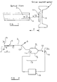
- Figure 1 schematically illustrates a silicon resonant sensor 1 comprising a diaphragm 8 supporting a vibratable element 4.
- the element 4 is contained within an evacuated cavity (not shown) and is illuminated by light supplied via an optical fibre 2.
- the fibre 2 need not directly address the vibrating element 4, but may shine light onto a reflecting surface formed at an angle of 45° to both the end of the fibre and the vibrating element 4.
- An example of a suitable vibrating element transducer is disclosed in US 5384872.
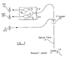
- a source S of substantially monochromatic light illuminates the vibrating element 4 and the partial reflector 6 via an optical fibre 2.
- Light returning from the vibrating element 4 and the partial reflector 6 is directed towards an interferometer 10 via a coupler 12.
- the interferometer 10 comprises a first interferometer optical path P 1 and a second interferometer optical path P 2 .
- a first portion L 1 of the light is reflected from the partial reflector 6 and a second portion L 2 of the light is reflected from the vibrating element 4.
- the second portion of light L 2 travels a further distance 2d compared to the first portion of light L 1 .
- the light L 1 + L 2 arriving at the interferometer 10 is split between the first and second interferometer paths P 1 and P 2 .
- the length of the second interferometer optical path P 2 is equal to P 1 + 2d.
- Light arriving at the output 15 of the interferometer 10 can have any one of four effective path lengths, these are:
- paths PL2 and PL3 are substantially the same length and therefore the portions of light which have travelled these respective paths can undergo mutual coherent interference.
- the other pairs of path lengths i.e. PL1 and PL3, PL1 and PL4, and PL2 and PL4, differ by 2d or more. Since 2d is a distance greater than the coherence length of the light from the source S, the light travelling via the above paths is not coherent at the output of the interferometer 10 and consequently does not undergo coherent interference. This light contributes to a general background level upon which an amplitude modulated signal representing the vibration of the vibrating element 4 is superimposed.
- the vibration of the vibrating element phase modulates light travelling via PL3 with respect to light travelling via PL2, so that the intensity of the radiation after interference varies with the vibration of the element 4.
- the interferometer can be tailored to compensate for different reflectivities at the partial reflector 6 and the vibrating element 4.
- losses at reflection from the vibrating element were such that 80% of the light reaching the interferometer 10 was received from the partial reflector 6 whereas only 20% of the light came from the vibrating element 4.
- the portions of light having effective path lengths PL2 and PL3 have been path length corrected so as to be able to undergo coherent interference, there is, as yet, no guarantee that the interference will give rise to a signal suitable for detecting motion of the vibrating element 4.
- the path lengths PL2 and PL3 should differ by (2n + 1) ⁇ /4.
- an electrically controllable path length adjusting element 14 can be inserted in one of the interferometer paths P 1 and P 2 .
- the effective path length adjusting element 14 need only be able to produce a path length change of ⁇ /4 in order to guarantee that the maximum sensitivity can be achieved.
- a photodetector 16 receives the output of the interferometer and supplies a signal to a controller 18.
- the controller 18 is arranged to control the path length change introduced by the electrically controllable path length adjuster 14 so as to maintain the interferometer 10 at a condition where motion of the vibrating element 4 can be readily detected.
- the controller 18 may be arranged to dither the control signal to the path length adjuster 14 in order to determine how the amplitude of the interference varies as a function of the signal applied to the effective path length adjusting means 14, and can thereby control the interferometer for maximum sensitivity.
- Such an arrangement may not respond quickly enough to rapid motion of the diaphragm 8, and may result in periods where the signal fades before the controller 18 is able to re-establish a suitable path length within the path length adjusting means 14.
- the arrangement shown in Figure 3 is similar to that shown in Figure 2 except that there are two interferometers, 10 and 20 optically in parallel.
- the second interferometer 20 comprises a third interferometer optical path and a fourth interferometer optical path.
- the length of the third interferometer optical path is equal to the length of the first interferometer optical path and the length of the fourth interferometer optical path differs from the length of the second interferometer optical path by ⁇ /4 (although in general this can be (2n +1) ⁇ /4 where n is an integer) where ⁇ is the wavelength of the monochromatic optical radiation emitted by the source S.
- neither interferometer 10 or 20 has an electrically controllable effective path length adjusting means in either of its optical paths.
- the action of the second interferometer 20 is as described with reference to the first interferometer 10.
- the change in the path length of the fourth optical path P 4 by ⁇ /4 compared to the second interferometer optical path P 2 means that the interferometers act in quadrature and that irrespective of the position of the diaphragm 8, at least one of the interferometers 10 and 20 will be able to resolve a signal indicative of the vibration of the element 4.
- the output of the first interferometer 10 is monitored by a first photodetector 16, whereas the output of the second interferometer 20 is monitored by a second photodetector 22.
- the first and second interferometers 10 and 20 may be formed as integrated components within a chip, as shown Figure 4.
- the chip comprises a silicon substrate 30 which has been masked and processed to define a series of waveguides as illustrated in Figure 4.
- Figure 4 shows the path lengths from an input portion 32 to the start 34 and 36 of each interferometer 10 and 20 as being identical, this is not in fact necessary.
- the distances which are critical are the path lengths P 1 and P 2 from the start 34 of the first interferometer to an output 38 thereof and the path lengths P 3 and P 4 from the start 36 of the second interferometer to an output 40 thereof. All other lengths within the chip may be freely chosen.
- Optical waveguides may be formed either on the surface of the substrate or embedded within e.g.
- Optically transparent materials may be deposited or chemically grown into the appropriate areas in order to form optical waveguides. Materials such as silica, doped silica, silicon oxynitride or other materials with appropriate optical properties can be used.
- the waveguide may comprise a core and a cladding so as to effectively confine light within the waveguide.
- the ⁇ /4 path difference inserted in one arm of one of the interferometers compared to the other interferometer provides a ⁇ /2 phase difference between the output signals of the first and second interferometers 10 and 20, respectively.
- ⁇ represents a phase shift introduced by the rest (non-vibrating) position of the element 4, which changes with distortion of the diaphragm.
- O 2 B(1 + cos ( ⁇ + ⁇ )).
- ⁇ varies slowly with position, there will be positions for each interferometer which provide virtually zero sensitivity to the small perturbations of the nominal gap distance d as a result of vibration of the vibrating element 4.
- the motion of the resonator can be continuously extracted by suitable processing of the output signals of the first and second interferometers.
- the output O 1 of the first interferometer 10 is monitored by a photodetector, converted to an electrical signal, and then passed through a high pass or band pass filter to remove DC components.
- the output O C includes a signal of the form R 2 cos 2 ( ⁇ R t) which is invariant of the gross or drift position ⁇ of the diaphragm.
- Figure 5 schematically illustrates a processing circuit for performing such a calculation in respect of the outputs of the first and second photodetectors 16 and 22 of the arrangement shown in Figures 3 and 4.
- An output of the first photodetector 16 is supplied to a first amplifier 50.
- An output of the amplifier 50 is supplied to an input of a band pass filter 52 arranged to pass signals at the expected vibrational frequency of the resonant element 4.
- An output of the band pass filter 52 is supplied to an input of a squaring element 54, such as a four quadrant multiplier.
- An output of the squaring element 54 is provided to a first input of a summer 56.
- an output of the photodetector 22 is processed by a further amplifier 58, a further band pass filter 60 and a further squaring element 62 before being supplied to a second input of the summer 56.
- the output signals of each interferometer may be cross multiplied with their respective time differentiated signals and the resultants summed to give a time differentiated modulation signal d ⁇ /dt.
- the modulation signal ⁇ R cos ( ⁇ RT ) is produced.
- FIG 6 shows a modification to the interferometer arrangement shown in Figure 4.
- the interferometer optical paths P 1 and P 3 have additional path length sections 70 and 72, respectively, formed therein. These additional path length sections are electrically controllable to change the effective path lengths of the first and third interferometer paths P 1 and P 3 , respectively.
- the sections 70 and 72 may be provided by an electro-strictive, piezo-optic, or a piezo-electric material, such as zinc oxide, lead zirconate or lead titanate. On application of a DC electric field to these sections, they will produce a stress induced path-length change in the portion of the waveguide formed by the section 70 or 72 and thus alter the effective path length in that interferometer arm.
- a heater strip can be deposited over a section of one interferometer arm using, for example, tin oxide to form the strip.
- tin oxide to form the strip.
- the interferometer arrangement fabricated within a chip may suffer from a drift in its operating characteristic due to thermal effects.
- the drift will manifest itself as a phase change between the two interferometer paths.
- the provision of the path length adjusting elements 70 and 72 enables such drifts to be compensated.
- Such a compensation can be achieved as follows.
- a low frequency signal (compared to that of the resonating element 4) is applied to the path length adjusting sections 70 and 72 in each of the interferometers.
- the low frequency signal will be a 1 kHz sinusoidal signal.
- a nominal phase difference of ⁇ /2 radians exists between the signals at the outputs of the first and second interferometers.
- the result of applying an electrical modulation signal to one arm of an interferometer is to modulate the interferometer's optical output.
- the result is a high frequency signal representing the oscillation of the vibrating element 4 contained within a modulating envelope of the 1 kHz signal. Since the interferometers operate in quadrature, the phase of the modulating envelopes of the optical output signals are out of phase with respect to one another by ⁇ /2 radians.
- a portion of the electrical signals may be tapped-off, fed into band pass filters centred at 1 kHz and then fed to a phase detection circuit, such as a phase sensitive detector PSD.
- the PSD produces an output signal which is proportional to the difference in phase between the two 1kHz modulation signals. So long as there is no drift between the optical path lengths of the two interferometers 10 and 20, the phase difference between the 1 kHz signals from the two interferometers will remain at ⁇ /2 radians.
- the phase difference between the 1 kHz signals will vary and consequently the output of the PSD will also vary.
- the PSD output signal can be conditioned to provide a DC voltage which varies linearly with the changes in phase. This DC signal can then be applied as a correcting signal to either or both of the additional path length correcting elements 70 and 72. When applying a DC signal to both elements 70 and 72, the DC signal applied to each element should be equal in magnitude but opposite in sign.
- Figure 7 schematically illustrates an apparatus for controlling the interferometer arrangement of Figure 6 to maintain the first and second interferometers in quadrature.
- Light at the output of the first interferometer 10 is converted to an electrical signal by a first photodetector 16.
- the output of the photodetector 16 is amplified by a first buffer amplifier 80.
- the output of the first buffer amplifier 80 is supplied to a first input of a phase sensitive detector 82 via a 1 kHz band pass filter 84.
- light at the output of the second interferometer 20 is converted into an electrical signal by a second photodetector 22.
- An output of the second photodetector 22 is supplied to a second buffer amplifier 86.
- An output of the second buffer amplifier 86 is supplied to a second input of the phase sensitive detector 82 via a second band pass filter 88.
- An output of the phase sensitive detector 82 is supplied to a first input of a first summing amplifier 90, and is inverted and applied to a first summing input of a second summing amplifier 92.
- Second summing inputs of the first and second summing amplifiers 90 and 92 receive a common signal from a signal generator 94.
- An output of the first summing amplifier 90 is used to control the first path length adjusting element 70, where as an output of the second summing amplifier 92 is used to control the second path length adjusting element 72. Electrical connections with the elements 70 and 72 are made via bonding pads 96a to 96d formed on the surface of the substrate 30.
- Another method for compensating for path length drift due to temperature variations is to deposit materials over the waveguide which produce an opposite effect to that of the temperature alone.
- a section of the waveguide undergoes a path length change which opposes the temperature drift and thus produces a cancelling effect.
- the chip carrying the first and second interferometers 10 and 20 may include optical fibre alignment grooves 100 for holding input and output optical fibres in proper alignment with the integrated optic waveguides 102 which form the interferometers 10 and 20.
- a section of the integrated optic waveguide is shown in greater detail in the insert in Figure 6.
- the integrated optic waveguide comprises a core 110 surrounded by a cladding material 112 which confines light to travel along the core 110.
- the interferometers may be formed within a semiconductor substrate such as silicon.
- the photodetectors and suitable processing electronics may also be fabricated on the substrate so as to provide a fully integrated detection system.
- Such an arrangement also simplifies the fabrication of the sensor head since the only requirement is that the path difference between the partial reflector 6 and vibrating element 4 is greater than the coherence length of the light used to illuminate the vibrating element 4. It is thus possible to provide a reliable detection system and a vibrating element transducer arrangement including such a detection system in which signal fading does not occur.
Landscapes
- Physics & Mathematics (AREA)
- General Physics & Mathematics (AREA)
- Instruments For Measurement Of Length By Optical Means (AREA)
Applications Claiming Priority (2)
| Application Number | Priority Date | Filing Date | Title |
|---|---|---|---|
| GB9505516 | 1995-03-18 | ||
| GBGB9505516.6A GB9505516D0 (en) | 1995-03-18 | 1995-03-18 | Optical signal retrieval apparatus and resonant sensor including such an apparatus |
Publications (2)
| Publication Number | Publication Date |
|---|---|
| EP0733888A1 true EP0733888A1 (fr) | 1996-09-25 |
| EP0733888B1 EP0733888B1 (fr) | 2002-01-09 |
Family
ID=10771449
Family Applications (1)
| Application Number | Title | Priority Date | Filing Date |
|---|---|---|---|
| EP96301378A Expired - Lifetime EP0733888B1 (fr) | 1995-03-18 | 1996-02-29 | Dispositif de mesure avec un élément vibrant |
Country Status (4)
| Country | Link |
|---|---|
| US (1) | US5991027A (fr) |
| EP (1) | EP0733888B1 (fr) |
| DE (1) | DE69618368D1 (fr) |
| GB (1) | GB9505516D0 (fr) |
Families Citing this family (3)
| Publication number | Priority date | Publication date | Assignee | Title |
|---|---|---|---|---|
| US6493490B1 (en) | 2000-12-18 | 2002-12-10 | Terabeam Corporation | Method and apparatus for receiving and aligning an optical communications beam with an integrated |
| US6721100B2 (en) * | 2001-11-07 | 2004-04-13 | Jds Uniphase Corporation | Sandwiched thin film optical filter |
| GB2509105B (en) * | 2012-12-20 | 2017-02-22 | Oxsensis Ltd | Mechanical resonator sensor |
Citations (2)
| Publication number | Priority date | Publication date | Assignee | Title |
|---|---|---|---|---|
| EP0419021A2 (fr) * | 1989-08-30 | 1991-03-27 | Schlumberger Industries Limited | Capteurs à éléments vibrants |
| EP0435553A2 (fr) * | 1989-12-29 | 1991-07-03 | Solartron Group Limited | Système à capteur optique |
-
1995
- 1995-03-18 GB GBGB9505516.6A patent/GB9505516D0/en active Pending
-
1996
- 1996-02-29 EP EP96301378A patent/EP0733888B1/fr not_active Expired - Lifetime
- 1996-02-29 DE DE69618368T patent/DE69618368D1/de not_active Expired - Lifetime
-
1998
- 1998-03-05 US US09/035,242 patent/US5991027A/en not_active Expired - Fee Related
Patent Citations (2)
| Publication number | Priority date | Publication date | Assignee | Title |
|---|---|---|---|---|
| EP0419021A2 (fr) * | 1989-08-30 | 1991-03-27 | Schlumberger Industries Limited | Capteurs à éléments vibrants |
| EP0435553A2 (fr) * | 1989-12-29 | 1991-07-03 | Solartron Group Limited | Système à capteur optique |
Also Published As
| Publication number | Publication date |
|---|---|
| GB9505516D0 (en) | 1995-05-03 |
| EP0733888B1 (fr) | 2002-01-09 |
| DE69618368D1 (de) | 2002-02-14 |
| US5991027A (en) | 1999-11-23 |
Similar Documents
| Publication | Publication Date | Title |
|---|---|---|
| US5280341A (en) | Feedback controlled differential fiber interferometer | |
| US4552457A (en) | Fiber optic interferometer using two wavelengths or variable wavelength | |
| KR940011933B1 (ko) | 측정자를 감지하기 위한 장치 및 방법 | |
| US4320475A (en) | Monomodal optical fibre hydrophone operating by the elastooptical effect | |
| KR910005546B1 (ko) | 안정화 광학 섬유 감지기 | |
| US4842358A (en) | Apparatus and method for optical signal source stabilization | |
| US5963034A (en) | Electro-optic electromagnetic field sensor system with optical bias adjustment | |
| EP0398085B1 (fr) | Procédé de mesurage de position très sensible | |
| US4799797A (en) | Coherence multiplexing of optical sensors | |
| US5034603A (en) | Integrated optics wavelength stabilization unit | |
| US4753529A (en) | Apparatus and method for precision adjustment of interferometer pathlength difference | |
| JPS59196403A (ja) | フアブリ・ペロ−形検知装置 | |
| JPH02257107A (ja) | エネルギフイルタ装置 | |
| US5167444A (en) | Apparatus and method for optical signal source stabilization | |
| Beheim et al. | Fiber‐linked interferometric pressure sensor | |
| JP3294376B2 (ja) | ファイバ光学センサ | |
| US20150308911A1 (en) | Mechanical resonator sensor | |
| US5583643A (en) | Methods of and apparatus for measurement using acousto-optic devices | |
| KR0153277B1 (ko) | 광대역 광섬유 진동 감지기 | |
| US4665363A (en) | Optical fibre magnetic gradient detector | |
| Shan et al. | New field formulas for the Fabry-Pérot interferometer and their application to ultrasound detection | |
| EP0733888B1 (fr) | Dispositif de mesure avec un élément vibrant | |
| JP3188528B2 (ja) | 交番電界及び交流電圧のための光ファイバーセンサ | |
| JPH05256769A (ja) | ガス濃度測定方法およびその測定装置 | |
| US4840489A (en) | Interferometer gyroscope having two feedback loops |
Legal Events
| Date | Code | Title | Description |
|---|---|---|---|
| PUAI | Public reference made under article 153(3) epc to a published international application that has entered the european phase |
Free format text: ORIGINAL CODE: 0009012 |
|
| AK | Designated contracting states |
Kind code of ref document: A1 Designated state(s): DE ES FR GB IT |
|
| 17P | Request for examination filed |
Effective date: 19970424 |
|
| RAP1 | Party data changed (applicant data changed or rights of an application transferred) |
Owner name: BOOKHAM TECHNOLOGY LIMITED |
|
| 17Q | First examination report despatched |
Effective date: 19990924 |
|
| RTI1 | Title (correction) |
Free format text: MEASURING APPARATUS WITH A VIBRATING ELEMENT |
|
| GRAG | Despatch of communication of intention to grant |
Free format text: ORIGINAL CODE: EPIDOS AGRA |
|
| RAP1 | Party data changed (applicant data changed or rights of an application transferred) |
Owner name: BOOKHAM TECHNOLOGY PLC |
|
| GRAG | Despatch of communication of intention to grant |
Free format text: ORIGINAL CODE: EPIDOS AGRA |
|
| GRAH | Despatch of communication of intention to grant a patent |
Free format text: ORIGINAL CODE: EPIDOS IGRA |
|
| GRAH | Despatch of communication of intention to grant a patent |
Free format text: ORIGINAL CODE: EPIDOS IGRA |
|
| GRAA | (expected) grant |
Free format text: ORIGINAL CODE: 0009210 |
|
| REG | Reference to a national code |
Ref country code: GB Ref legal event code: IF02 |
|
| AK | Designated contracting states |
Kind code of ref document: B1 Designated state(s): DE ES FR GB IT |
|
| PG25 | Lapsed in a contracting state [announced via postgrant information from national office to epo] |
Ref country code: IT Free format text: LAPSE BECAUSE OF FAILURE TO SUBMIT A TRANSLATION OF THE DESCRIPTION OR TO PAY THE FEE WITHIN THE PRESCRIBED TIME-LIMIT;WARNING: LAPSES OF ITALIAN PATENTS WITH EFFECTIVE DATE BEFORE 2007 MAY HAVE OCCURRED AT ANY TIME BEFORE 2007. THE CORRECT EFFECTIVE DATE MAY BE DIFFERENT FROM THE ONE RECORDED. Effective date: 20020109 Ref country code: FR Free format text: LAPSE BECAUSE OF FAILURE TO SUBMIT A TRANSLATION OF THE DESCRIPTION OR TO PAY THE FEE WITHIN THE PRESCRIBED TIME-LIMIT Effective date: 20020109 |
|
| REF | Corresponds to: |
Ref document number: 69618368 Country of ref document: DE Date of ref document: 20020214 |
|
| PG25 | Lapsed in a contracting state [announced via postgrant information from national office to epo] |
Ref country code: GB Free format text: LAPSE BECAUSE OF NON-PAYMENT OF DUE FEES Effective date: 20020409 |
|
| PG25 | Lapsed in a contracting state [announced via postgrant information from national office to epo] |
Ref country code: DE Free format text: LAPSE BECAUSE OF FAILURE TO SUBMIT A TRANSLATION OF THE DESCRIPTION OR TO PAY THE FEE WITHIN THE PRESCRIBED TIME-LIMIT Effective date: 20020410 |
|
| PG25 | Lapsed in a contracting state [announced via postgrant information from national office to epo] |
Ref country code: ES Free format text: LAPSE BECAUSE OF FAILURE TO SUBMIT A TRANSLATION OF THE DESCRIPTION OR TO PAY THE FEE WITHIN THE PRESCRIBED TIME-LIMIT Effective date: 20020730 |
|
| EN | Fr: translation not filed | ||
| PLBE | No opposition filed within time limit |
Free format text: ORIGINAL CODE: 0009261 |
|
| STAA | Information on the status of an ep patent application or granted ep patent |
Free format text: STATUS: NO OPPOSITION FILED WITHIN TIME LIMIT |
|
| GBPC | Gb: european patent ceased through non-payment of renewal fee |
Effective date: 20020409 |
|
| 26N | No opposition filed |