EP0734045A2 - Appareil à faisceau d'ions focalisé et méthode d'irradiation par faisceau d'ions focalisés - Google Patents
Appareil à faisceau d'ions focalisé et méthode d'irradiation par faisceau d'ions focalisés Download PDFInfo
- Publication number
- EP0734045A2 EP0734045A2 EP96103903A EP96103903A EP0734045A2 EP 0734045 A2 EP0734045 A2 EP 0734045A2 EP 96103903 A EP96103903 A EP 96103903A EP 96103903 A EP96103903 A EP 96103903A EP 0734045 A2 EP0734045 A2 EP 0734045A2
- Authority
- EP
- European Patent Office
- Prior art keywords
- sample
- ion
- ion source
- ion beam
- objective lens
- Prior art date
- Legal status (The legal status is an assumption and is not a legal conclusion. Google has not performed a legal analysis and makes no representation as to the accuracy of the status listed.)
- Withdrawn
Links
- 238000010884 ion-beam technique Methods 0.000 title claims abstract description 58
- 238000000034 method Methods 0.000 title claims abstract description 15
- 230000001678 irradiating effect Effects 0.000 title description 4
- 238000003801 milling Methods 0.000 claims abstract description 58
- 230000003287 optical effect Effects 0.000 claims abstract description 36
- 229910001338 liquidmetal Inorganic materials 0.000 claims description 2
- 150000002500 ions Chemical class 0.000 claims 17
- 238000004458 analytical method Methods 0.000 abstract description 23
- 239000004065 semiconductor Substances 0.000 abstract description 18
- 230000008569 process Effects 0.000 abstract description 4
- 238000011156 evaluation Methods 0.000 abstract description 3
- 230000007423 decrease Effects 0.000 description 8
- 230000014509 gene expression Effects 0.000 description 5
- 239000010409 thin film Substances 0.000 description 5
- 230000004075 alteration Effects 0.000 description 4
- 238000000605 extraction Methods 0.000 description 4
- 239000002245 particle Substances 0.000 description 4
- 238000002360 preparation method Methods 0.000 description 4
- 230000008859 change Effects 0.000 description 3
- 238000005520 cutting process Methods 0.000 description 3
- 238000004544 sputter deposition Methods 0.000 description 3
- 230000005540 biological transmission Effects 0.000 description 2
- 238000004364 calculation method Methods 0.000 description 2
- 230000003247 decreasing effect Effects 0.000 description 2
- 238000013461 design Methods 0.000 description 2
- 230000000694 effects Effects 0.000 description 2
- 238000004519 manufacturing process Methods 0.000 description 2
- GYHNNYVSQQEPJS-UHFFFAOYSA-N Gallium Chemical compound [Ga] GYHNNYVSQQEPJS-UHFFFAOYSA-N 0.000 description 1
- 230000003466 anti-cipated effect Effects 0.000 description 1
- 238000005452 bending Methods 0.000 description 1
- 238000010276 construction Methods 0.000 description 1
- 238000000151 deposition Methods 0.000 description 1
- 230000008021 deposition Effects 0.000 description 1
- 238000010586 diagram Methods 0.000 description 1
- 238000005516 engineering process Methods 0.000 description 1
- 238000002474 experimental method Methods 0.000 description 1
- 239000010408 film Substances 0.000 description 1
- 229910052733 gallium Inorganic materials 0.000 description 1
- 230000006872 improvement Effects 0.000 description 1
- 238000007689 inspection Methods 0.000 description 1
- 230000007246 mechanism Effects 0.000 description 1
- 230000004048 modification Effects 0.000 description 1
- 238000012986 modification Methods 0.000 description 1
- 238000005457 optimization Methods 0.000 description 1
- 230000009467 reduction Effects 0.000 description 1
- 239000011163 secondary particle Substances 0.000 description 1
- 230000000007 visual effect Effects 0.000 description 1
Images


Classifications
-
- H—ELECTRICITY
- H01—ELECTRIC ELEMENTS
- H01J—ELECTRIC DISCHARGE TUBES OR DISCHARGE LAMPS
- H01J37/00—Discharge tubes with provision for introducing objects or material to be exposed to the discharge, e.g. for the purpose of examination or processing thereof
- H01J37/30—Electron-beam or ion-beam tubes for localised treatment of objects
- H01J37/3002—Details
- H01J37/3007—Electron or ion-optical systems
-
- H—ELECTRICITY
- H01—ELECTRIC ELEMENTS
- H01J—ELECTRIC DISCHARGE TUBES OR DISCHARGE LAMPS
- H01J37/00—Discharge tubes with provision for introducing objects or material to be exposed to the discharge, e.g. for the purpose of examination or processing thereof
- H01J37/30—Electron-beam or ion-beam tubes for localised treatment of objects
- H01J37/3002—Details
- H01J37/3005—Observing the objects or the point of impact on the object
-
- H—ELECTRICITY
- H01—ELECTRIC ELEMENTS
- H01J—ELECTRIC DISCHARGE TUBES OR DISCHARGE LAMPS
- H01J2237/00—Discharge tubes exposing object to beam, e.g. for analysis treatment, etching, imaging
- H01J2237/30—Electron or ion beam tubes for processing objects
- H01J2237/317—Processing objects on a microscale
- H01J2237/3174—Etching microareas
- H01J2237/31742—Etching microareas for repairing masks
Definitions
- the present invention is related to a focused ion beam (FIB) apparatus.
- FIB focused ion beam
- focused ion beam apparatus is used in various fields.
- the apparatus is used for applications in a micro area because its fine focused beam can be applied to an extremely small area.
- the focused ion beam apparatus which focuses ion beam from an ion source through a lens and irradiates the beam onto a sample, is also used for milling and observing a sample in a micro area.
- the focused ion beam is also used for failure analysis of semiconductors.
- Semiconductors have been integrated these years, and they have a layered structure. For this reason, to inspect a semiconductor, it is necessary to make a required layer exposed and then inspect the surface condition of the layer. Because the focused ion beam is applicable to both milling and observation, it is suitable for failure analysis of semiconductors. First, increase current of the ion beam and mill from the surface down to a required layer of a semiconductor. Then, decrease current of the ion beam and inspect surface condition of the layer.
- the total optical ion-beam path length Lt from the tip of the ion emitter of the ion source 1 to the sample 10 is 275 mm.
- Distance Lo from the ion source to the condenser lens center is 25 mm
- distance L from the condenser lens center to the objective lens center is 220 mm
- distance Li from the objective lens center to the sample is 30 mm.
- a focused ion beam apparatus is associated with a problem in the milling mode that, if the focused ion beam is not fine enough, the beam cannot mill a fine pattern of a semiconductor in failure analysis.
- Another problem in the milling mode is that milling speed decreases if current of the ion beam is not high enough.
- the beam position is affected by drift of the sample stage, and accordingly the focused beam cannot be fit to a fine pattern of a semiconductor.
- the focused ion beam apparatus is associated with another problem that, if the focused ion beam is not fine enough, the apparatus cannot observe a fine pattern of a semiconductor in failure analysis.
- Another problem in the observing mode is that, if current of the ion beam is not high enough, attained signals are too low to detect an image with sufficient S/N ratio.
- the focused ion beam apparatus does not solve these problems and it is impossible to use the apparatus for failure analysis of semiconductors.
- the object of the present invention is to furnish a focused ion beam apparatus that enables to carry out failure analysis of semiconductors with fine patterns.
- the inventor of the present invention has repeated analyses and experiments on failure analysis of semiconductors, particularly on ion beam diameter and ion beam current and found out that the following conditions are required for failure analysis of semiconductors, particularly, 64M byte DRAM and 256M byte DRAM.
- components of the focused ion beam apparatus of the present invention which comprises an ion source, a condenser lens for focusing ion beam from said ion source, and an objective lens, are arranged so that the total optical path length from the tip of the emitter of said ion source to said sample is within a range of from 300 to 450 mm and distance from said objective lens center to said sample is 40 mm or less.
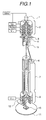
- Figure 1 shows the construction of the optical ion beam system of the focused ion beam apparatus in the present invention.
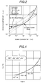
- Figure 2 shows a relation curve of beam diameter versus beam current (Dp-Ip) in the present invention.
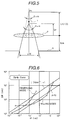
- Figures 3A and 3B shows a schematic diagram of the optical ion beam system in the present invention.
- Figure 4 shows common relation curve of beam diameter versus beam current (Dp-Ip).
- Figure 5 shows a relation curve of half-angle of the incoming and outgoing beam versus aperture size of the beam defining aperture size of the observation beam in the preferred embodiment of the present invention.
- Figure 6 shows a characteristic curve of beam diameter versus beam current (Dp-Ip) of the FIB apparatus in the preferred embodiment of the present invention.
- Figure 7 shows the FIB sample preparation procedure for a TEM sample and sectional figure of the sample.
- FIG. 1 is an assembly drawing showing the brief structural elements of the ion optical system of the FIB apparatus.
- the ion source 1 is a liquid metal ion source (LMIS) using high brightness gallium (Ga).
- LMIS liquid metal ion source
- Ga gallium
- the ion emitted from the ion source 1 is focused onto a sample 10 held by a sample stage 11 by a condenser lens 2 and an objective lens 8.
- the beam diameter of the focused ion beam (FIB) 9 is defined by a beam defining aperture 3 located immediately behind the condenser lens 2.
- the beam transmits an aligner/stigmator 4, a blanker 5, a blanking plate 6, and is scanned on the sample 10 by an electrostatic deflector 7. Charged particles emitted from the sample 10 are detected by a charged-particle detector 12.
- the lens centre must, in general, be defined at a position where the lens effect is greatest, i.e. at the centre between the principal planes of the front and rear lenses, the lens centre in this description is defined by approximation using thin lenses.
- the condenser lens in the disclosed prior art consists of four electrodes with 10 mm gap between each electrode.
- the condenser lens center is defined to be located at the position of the third electrode from the ion source.
- the objective lens consists of three electrodes with 10 mm gap between each electrode, and the objective lens center is defined to be located at the position of the middle electrode.
- Mode change by switching the condenser lens is as follows. Two different focusing modes are available by switching the second and third electrodes of the condenser lens; that is, (a) high current intensity beam mode for FIB milling and (b) fine beam mode for image observation by a scanning ion microscope (SIM).
- SIM scanning ion microscope
- the total optical ion beam path length from the tip of the ion emitter of the ion source 1 to the sample 10 is 275 mm, wherein distance Lo from the ion source to the condenser lens center is 25 mm, distance L from the condenser lens center to the objective lens center is 220 mm, and distance Li from the objective lens center to the sample is 30 mm.
- Figure 2 shows a curve of beam diameter Dp versus beam current Ip for both the FIB milling mode and SIM image observing mode.
- the milling beam diameter Dp is switched from large to small in a range of 50 nm to 1 ⁇ m, depending upon the area to be milled, to conduct rough, medium, and fine milling.
- the optical system is a two-lens system, wherein distance from the condenser lens center to the tip of the ion emitter is defined as Lo, distance from the condenser lens center to the objective lens center is as L, and distance from the objective lens center to the sample is as Li.
- the sum of these distances ( Lo + L + Li ) is defined as the total optical path length Lt.
- Distance from the condenser lens center to the beam defining aperture is defined as P1.
- the tip of the ion emitter is defined as the object point of the condenser lens and the image point of the condenser lens is defined as P1.
- the crossover mode when the image point P1 is positioned between the two lenses, it is called the crossover mode, and when P2 is positioned out of the two lenses, it is called the collimating mode.
- Figures 3(a) and 3(b) shows the crossover mode and collimating mode, respectively. The latter shows how the beam is focused when the image point P1 is positioned on the ion source side.
- Vo ion extraction potential Ve
- Vi Vi
- the origin of the potential is set at the ion emitter.
- the sample is normally at the earth potential and ion accelerating voltage is applied to the ion emitter.
- Figure 4 shows a normal Dp-Ip characteristic curve that is attained when the optical path length and potential are fixed and the beam half-angle ⁇ o on the incidence side of the condenser lens constituting the FIB is changed.
- the beam diameter Dp is expressed as follows using the Gaussien image size dg, deviation of image due to chromatic aberration dc, and deviation of image due to spherical aberration ds.
- Dp 2 dg 2 + dc 2 + ds 2
- dg, dc, and ds can be expressed as follows, respectively, using the lens magnification Mt, virtual source size Ds, and chromatic and spherical aberration coefficients (Cc and Cs, respectively).
- ⁇ V is a voltage converted from ⁇ E and Vo is the ion extraction voltage.
- Hc is a proportional term determined only by the optical path length and potential of the optical system in dc.
- Mcl and Mol are the lens magnification of the condenser lens and objective lens, respectively.
- Ip Ja ( ⁇ o 2 )
- the characteristic curve shows the following three features.
- the ion source operating conditions Ja, Ds, and ⁇ V
- optical path lengths Li, L, and Li
- Increasing Jmax of the milling beam means nothing but optimizing the set position of the image point P1, that is, optimizing L1/L2 to minimize
- the optimized value of L1/L2 is expressed by the equation 9 using the average voltage of the condenser lens and objective lens (Vavc and Vavo, respectively) (Deductive expressions used in the course of calculation are omitted).
- Hc and Mt are expressed by the equations 10 and 11, respectively, where it is assumed that Lo ⁇ L and Li ⁇ L.
- L1/L2 ⁇ [(Lo/Li)(Vavc/Vavo)] 1/2
- Hc ⁇ 4[(Vo/Vi) 1/4 (LiLo)] 1/2 /(Vavc ⁇ Vavo) 1/2
- Mt ⁇ 4(Vo/Vi) 1/4 (Li/Lo) 1/2 /(Vavc/Vavo) 1/2
- the collimating mode is selected for focusing of the observation beam, partly because of requirement of the beam defining aperture as described later in item (3), and the image point P1 is moved toward the ion source to make a virtual image point so that
- the condenser lens is made to function mostly as an accelerating device rather than a focusing device.
- Li/L2 Mt/Mc1 ⁇ (6 ⁇ 17)
- 2 (L2 + Li)/Vavo ⁇ 2Lt/Vavo
- Position and aperture size of the beam defining aperture are examined hereunder.
- the observation beam requires the smallest aperture size.
- the aperture functions to limit quantity of the beam passing through it, a beam colliding with side walls of the aperture changes to a scattered beam which becomes a thick noise beam on a sample. From a viewpoint of reducing this scattered beam, thickness of the aperture needs to be thinnest possible.
- the life of the aperture depends upon its thickness because the aperture is etched by an irradiating beam due to sputtering. Accordingly, from a viewpoint of increasing the life of an aperture, thickness of the aperture needs to be thickest possible.
- repeatable positioning accuracy of the aperture is required to be almost equal to or less than the aperture size.
- the repeatable positioning accuracy of an aperture with simple mechanism designed to meet cost reduction requirement is about 10 ⁇ m. Accordingly, it is desirable to set the minimum aperture size to 10 ⁇ m or greater from a viewpoint of repeatability of the positioning accuracy.
- the minimum aperture size is set to about 10 ⁇ m.
- Ip ( ⁇ /4)Ja(Vm/Vo) 1/2 W 2 / ⁇ Lo+Lca/(-L1/Lo) ⁇ 2
- Lo 15 to 45 mm
- thickness of the lenses should be not less than 15 mm considering at least 20 kV of the accelerating voltage.
- a space for extracting the ion from the ion source to the condenser lens where the ion extraction voltage is from 6 to 9 kV is needed. Therefore, the minimum value 15 mm as the optical path length Lo is obtained by summing the space distance for the extracting voltage and a half of the lens thickness.
- the distance from the condenser lens to the sample should be more than a space for bending the moving orbit of the charged particle towards transverse direction for detecting the charged particle such as secondary electron or secondary ion and a separating distance for obtaining at least 100 ⁇ m as a practical deflection distance of the beam on the sample.
- the optical path length L1 becomes at least 10 mm obtained as a sum of the space distance and the half of the lens thickness.
- the optical path length (Lo + Lca) from the ion source to the beam defining aperture becomes at least 55 mm in order to satisfying the requirement (8).
- the optical path length from the ion source to the beam defining aperture becomes at least about 245 mm and is obtained as a total sum of minimum value 10 mm of the optical path length Li, the distance between the aligner/stigmator, the blanker and the deflector, and the half of the thickness of the condenser lens. Therefore, the total optical path length Lt from the ion source to the sample becomes at least about 300 mm.
- Vi is increased when Vi is increased, higher Vi results in higher applied voltage to the lenses and consequently cost of the ion source and accelerating power source increases.
- a range to be scanned by the beam on a sample become narrower in reverse proportion to Vi. Accordingly, the maximum value of Vi is 40 kV from a viewpoint of practical use.
- Vi which is normally 30 kV was lowered one-half to 15 kV and the maximum beam scanning distance was doubled (area of the visual field was increased by four times).
- Vi needs to be above 20 kV to increase sputtering yield. In view of the above, Vi is set to a range of 20 to 40 kV.
- the deflector is positioned in two different methods. One is a succeeding deflection method, where the deflector is positioned just after the objective lens. The other is a preceding deflection method, where the deflector is positioned just before the objective lens.
- the former method is available only when Li is long but the latter method is available even if Li is short. For the latter, it is necessary to let the beam pass through the center of the objective lens regardless of amount of deflection. For this reason, the deflector needs to be a two-stage type and more complicated structural design and electrical control are required, which is disadvantageous.
- employing the preceding deflection method with shorter Li is advantageous.
- the second apparatus of the embodiment of the present invention is exactly the same as the above-described first apparatus of the embodiment except that Lo is changed to 45 to 80 mm and Lca to 130 mm.
- Beam characteristic of the second apparatus as compared to that of the first apparatus is that Jmax is slightly lower but that the fine milling beam can be narrowed much more. This result can also be anticipated from equations 10 and 11. Because Jmax and the minimum beam diameter trade off each other, it is advantageous to set Lo longer if importance is particularly attached to the minimum beam diameter.
- the third apparatus of the embodiment of the present invention is exactly the same as the above-described first apparatus of the embodiment except that Lt is changed to 550 mm.
- Beam characteristic of the third apparatus as compared to that of the first apparatus is that Jmax is slightly lower but that much finer beam diameter can be realized because the lens magnification of the observation beam can be decreased further. This is particularly advantageous for observing high resolution SIM image.
- the maximum current intensity Jmax is increased by more than 50% and the beam diameter is narrowed by about 20% for the fine milling beam and by more than 50% for the observing mode.
- This improvement makes it possible to conduct FIB milling to higher accuracy at higher speed and observe SIM image in higher resolution, thus enabling to conduct failure analysis and process evaluation of functional fine elements to higher accuracy and for greater throughput.
- reliability in sample preparation for transmission electron microscope is remarkably improved because yield of sample preparation is improved from about 70% in the past to 90% or higher.
- the improved beam characteristic of the present invention helps achieve high positioning accuracy, high throughput and high reliability not only in the above-described failure analysis and process inspection but in device modification employing wire cutting by FIB milling and wire connection by FIB-assisted deposition.
- FIG. 7 shows procedure for the FIB milling.
- a sample is milled across two sections by the rough milling beam so that a thin film of several ⁇ m thick including a portion to be subjected to TEM observation is left over.
- Dp and Ip for the rough, medium, and fine milling are 0.5 to 2 ⁇ m and 8 to 15 nA, 0.1 to 0.5 ⁇ m and 0.2 to 8 nA, and 50 to 60 nm and 50 to 80 pA, respectively.
- Time required for the medium milling is 1 to 2 hours and that for the fine milling is 0.3 to 1 hour.
- Total hours of milling including the rough milling are 1.5 to 3 hours. Section of the thin film sample after final finish is checked by SIM observation using much finer observation beam, and then the sample is subjected to the TEM observation.
- positioning accuracy of the FIB milling is in proportion to Dp and milling speed is in inverse proportion to Ip. Therefore, increase of the FIB current intensity contributes to high accuracy milling and high speed milling. That is to say, if Dp is the same (positioning accuracy of milling is the same), the milling speed is faster and milling can be completed in a shorter time when Ip is greater. On the other hand, if Ip is the same (milling speed is the same), positioning accuracy of the milling is higher when Dp is smaller. Reduced milling time contributes to the positioning accuracy of final finish because shorter milling time helps reduce drift of beam position and sample stage. Further, finer beam diameter improves image resolution and higher Ip improves image quality in the SIM image observation.
- Recent functional elements begin to employ finer patterns and three-dimensional structure. Accordingly, it is essential in failure analysis and process evaluation to conduct sectional milling and structural observation at a required portion of a sample. Since there is no other apparatus than an FIB apparatus available at present that can serve the purpose, the FIB milling to higher accuracy at higher speed and SIM image observation in higher resolution are keenly desired.
- the present invention brings an effect of enabling to realize failure analysis of semiconductors.
Landscapes
- Chemical & Material Sciences (AREA)
- Analytical Chemistry (AREA)
- Electron Sources, Ion Sources (AREA)
- Analysing Materials By The Use Of Radiation (AREA)
Applications Claiming Priority (2)
| Application Number | Priority Date | Filing Date | Title |
|---|---|---|---|
| JP06551195A JP3265901B2 (ja) | 1995-03-24 | 1995-03-24 | 集束イオンビーム装置及び集束イオンビーム照射方法 |
| JP65511/95 | 1995-03-24 |
Publications (2)
| Publication Number | Publication Date |
|---|---|
| EP0734045A2 true EP0734045A2 (fr) | 1996-09-25 |
| EP0734045A3 EP0734045A3 (fr) | 1997-11-12 |
Family
ID=13289158
Family Applications (1)
| Application Number | Title | Priority Date | Filing Date |
|---|---|---|---|
| EP96103903A Withdrawn EP0734045A3 (fr) | 1995-03-24 | 1996-03-12 | Appareil à faisceau d'ions focalisé et méthode d'irradiation par faisceau d'ions focalisés |
Country Status (3)
| Country | Link |
|---|---|
| US (1) | US5852297A (fr) |
| EP (1) | EP0734045A3 (fr) |
| JP (1) | JP3265901B2 (fr) |
Cited By (1)
| Publication number | Priority date | Publication date | Assignee | Title |
|---|---|---|---|---|
| WO2009155272A3 (fr) * | 2008-06-20 | 2010-03-18 | Carl Zeiss Smt. Inc. | Systèmes et procédés de coupe transversale |
Families Citing this family (19)
| Publication number | Priority date | Publication date | Assignee | Title |
|---|---|---|---|---|
| EP0840940B1 (fr) * | 1995-07-25 | 2000-06-14 | Nmi Naturwissenschaftliches Und Medizinisches Intitut An Der Universität Tübingen In Reutlingen | Procede et dispositif pour l'amincissement ionique dans un microscope electronique a transmission haute resolution |
| KR100401534B1 (ko) * | 1997-08-30 | 2003-12-24 | 주식회사 하이닉스반도체 | Esd 손상 위치 검출 방법 |
| US5969355A (en) * | 1997-09-04 | 1999-10-19 | Seiko Instruments Inc. | Focused ion beam optical axis adjustment method and focused ion beam apparatus |
| EP1210723B1 (fr) * | 2000-01-21 | 2009-03-18 | Fei Company | Faisceaux ioniques focalises modeles et a faible densite |
| JP3597761B2 (ja) * | 2000-07-18 | 2004-12-08 | 株式会社日立製作所 | イオンビーム装置及び試料加工方法 |
| US7084399B2 (en) * | 2000-07-18 | 2006-08-01 | Hitachi, Ltd. | Ion beam apparatus and sample processing method |
| US6977386B2 (en) * | 2001-01-19 | 2005-12-20 | Fei Company | Angular aperture shaped beam system and method |
| US7786451B2 (en) | 2003-10-16 | 2010-08-31 | Alis Corporation | Ion sources, systems and methods |
| US7786452B2 (en) | 2003-10-16 | 2010-08-31 | Alis Corporation | Ion sources, systems and methods |
| US9159527B2 (en) | 2003-10-16 | 2015-10-13 | Carl Zeiss Microscopy, Llc | Systems and methods for a gas field ionization source |
| US8110814B2 (en) | 2003-10-16 | 2012-02-07 | Alis Corporation | Ion sources, systems and methods |
| JP4338593B2 (ja) * | 2004-06-15 | 2009-10-07 | 株式会社日立ハイテクノロジーズ | 集束イオンビーム装置 |
| JP4611755B2 (ja) * | 2005-01-13 | 2011-01-12 | 株式会社日立ハイテクノロジーズ | 走査電子顕微鏡及びその撮像方法 |
| JP5142240B2 (ja) * | 2006-01-17 | 2013-02-13 | 株式会社日立ハイテクノロジーズ | 荷電ビーム装置及び荷電ビーム加工方法 |
| US7804068B2 (en) | 2006-11-15 | 2010-09-28 | Alis Corporation | Determining dopant information |
| EP2122655A2 (fr) * | 2007-02-22 | 2009-11-25 | Applied Materials Israel Ltd. | Microscope électronique à balayage à fort rendement |
| DE102008064781B3 (de) * | 2007-04-23 | 2016-01-07 | Hitachi High-Technologies Corporation | lonenstrahlbearbeitungs-/Betrachtungsvorrichtung |
| US8101911B2 (en) * | 2008-11-04 | 2012-01-24 | ICT Integrated Circuit Testing Gesellschaft für Halbleiterprüftechnik mbH | Method and device for improved alignment of a high brightness charged particle gun |
| JP5952048B2 (ja) * | 2012-03-23 | 2016-07-13 | 株式会社日立ハイテクサイエンス | イオンビーム装置 |
Family Cites Families (5)
| Publication number | Priority date | Publication date | Assignee | Title |
|---|---|---|---|---|
| US4426582A (en) * | 1980-01-21 | 1984-01-17 | Oregon Graduate Center | Charged particle beam apparatus and method utilizing liquid metal field ionization source and asymmetric three element lens system |
| US4687940A (en) * | 1986-03-20 | 1987-08-18 | Hughes Aircraft Company | Hybrid focused-flood ion beam system and method |
| JP2708547B2 (ja) * | 1989-05-10 | 1998-02-04 | 株式会社日立製作所 | デバイス移植方法 |
| JP2774884B2 (ja) * | 1991-08-22 | 1998-07-09 | 株式会社日立製作所 | 試料の分離方法及びこの分離方法で得た分離試料の分析方法 |
| US5504340A (en) * | 1993-03-10 | 1996-04-02 | Hitachi, Ltd. | Process method and apparatus using focused ion beam generating means |
-
1995
- 1995-03-24 JP JP06551195A patent/JP3265901B2/ja not_active Expired - Lifetime
-
1996
- 1996-03-12 EP EP96103903A patent/EP0734045A3/fr not_active Withdrawn
- 1996-03-22 US US08/620,764 patent/US5852297A/en not_active Expired - Lifetime
Cited By (2)
| Publication number | Priority date | Publication date | Assignee | Title |
|---|---|---|---|---|
| WO2009155272A3 (fr) * | 2008-06-20 | 2010-03-18 | Carl Zeiss Smt. Inc. | Systèmes et procédés de coupe transversale |
| US8384029B2 (en) | 2008-06-20 | 2013-02-26 | Carl Zeiss Nts, Llc | Cross-section systems and methods |
Also Published As
| Publication number | Publication date |
|---|---|
| JP3265901B2 (ja) | 2002-03-18 |
| JPH08264150A (ja) | 1996-10-11 |
| EP0734045A3 (fr) | 1997-11-12 |
| US5852297A (en) | 1998-12-22 |
Similar Documents
| Publication | Publication Date | Title |
|---|---|---|
| EP0734045A2 (fr) | Appareil à faisceau d'ions focalisé et méthode d'irradiation par faisceau d'ions focalisés | |
| US7223983B2 (en) | Charged particle beam column | |
| US6674075B2 (en) | Charged particle beam apparatus and method for inspecting samples | |
| EP1045425B1 (fr) | Appareil à faisceaux de particules chargées avec compensation de l'aberration chromatique | |
| US4758723A (en) | Electron spectrometer | |
| EP0872873B1 (fr) | Microscope électronique à balayage | |
| Veneklasen | Design of a spectroscopic low-energy electron microscope | |
| EP1305816B1 (fr) | Collecte d'electrons secondaires a travers l'objectif d'un microscope electronique a balayage | |
| US20090321634A1 (en) | Multi-beam ion/electron spectra-microscope | |
| US7067807B2 (en) | Charged particle beam column and method of its operation | |
| US7235798B2 (en) | Focused ion beam apparatus | |
| JP3333533B2 (ja) | 荷電粒子抽出装置 | |
| JPH0286036A (ja) | イオンマイクロアナライザ | |
| US7022987B2 (en) | Particle-optical arrangements and particle-optical systems | |
| JP3867048B2 (ja) | モノクロメータ及びそれを用いた走査電子顕微鏡 | |
| EP0952606B1 (fr) | Dispositif compensé de lentille objectif-détecteur et méthode | |
| US5220167A (en) | Multiple ion multiplier detector for use in a mass spectrometer | |
| EP1105913B1 (fr) | Microscope electronique | |
| EP0150089A1 (fr) | Systèmes optiques pour particules chargées | |
| EP0617453A1 (fr) | Analyseur de particules chargées | |
| Ishitani et al. | Proposals for exact-point transmission-electron microscopy using focused ion beam specimen-preparation technique | |
| Griffith et al. | Low‐energy electron microscopy (LEEM) and mirror electron microscopy (MEM) of biological specimens: Preliminary results with a novel beam separating system | |
| JP2000277049A (ja) | カソードレンズ | |
| Sato et al. | An evaluation for the depth of field in SEM image depending on accelerating voltage | |
| Lencova | Accurate FOFEM computations and ray tracing in particle optics |
Legal Events
| Date | Code | Title | Description |
|---|---|---|---|
| PUAI | Public reference made under article 153(3) epc to a published international application that has entered the european phase |
Free format text: ORIGINAL CODE: 0009012 |
|
| AK | Designated contracting states |
Kind code of ref document: A2 Designated state(s): DE FR GB |
|
| PUAL | Search report despatched |
Free format text: ORIGINAL CODE: 0009013 |
|
| AK | Designated contracting states |
Kind code of ref document: A3 Designated state(s): DE FR GB |
|
| 17P | Request for examination filed |
Effective date: 19980430 |
|
| 17Q | First examination report despatched |
Effective date: 19990421 |
|
| STAA | Information on the status of an ep patent application or granted ep patent |
Free format text: STATUS: THE APPLICATION IS DEEMED TO BE WITHDRAWN |
|
| 18D | Application deemed to be withdrawn |
Effective date: 20020910 |