EP0734986A2 - Dispositif pour détecter sans contact la position d'une bande de matériau en mouvement - Google Patents
Dispositif pour détecter sans contact la position d'une bande de matériau en mouvement Download PDFInfo
- Publication number
- EP0734986A2 EP0734986A2 EP96104765A EP96104765A EP0734986A2 EP 0734986 A2 EP0734986 A2 EP 0734986A2 EP 96104765 A EP96104765 A EP 96104765A EP 96104765 A EP96104765 A EP 96104765A EP 0734986 A2 EP0734986 A2 EP 0734986A2
- Authority
- EP
- European Patent Office
- Prior art keywords
- electrode
- electrodes
- detector
- detector electrode
- potential
- Prior art date
- Legal status (The legal status is an assumption and is not a legal conclusion. Google has not performed a legal analysis and makes no representation as to the accuracy of the status listed.)
- Granted
Links
- 239000000463 material Substances 0.000 claims abstract description 50
- 238000001514 detection method Methods 0.000 claims abstract description 12
- 230000008878 coupling Effects 0.000 claims abstract description 7
- 238000010168 coupling process Methods 0.000 claims abstract description 7
- 238000005859 coupling reaction Methods 0.000 claims abstract description 7
- 238000011156 evaluation Methods 0.000 claims description 13
- 230000005540 biological transmission Effects 0.000 claims description 4
- 230000000694 effects Effects 0.000 claims description 4
- 238000009413 insulation Methods 0.000 claims description 4
- 239000004020 conductor Substances 0.000 claims description 2
- 230000001105 regulatory effect Effects 0.000 claims description 2
- 239000000725 suspension Substances 0.000 claims description 2
- 230000002093 peripheral effect Effects 0.000 claims 1
- 238000006073 displacement reaction Methods 0.000 abstract description 11
- 230000035945 sensitivity Effects 0.000 abstract description 8
- 239000012212 insulator Substances 0.000 description 3
- 238000012544 monitoring process Methods 0.000 description 3
- 230000003321 amplification Effects 0.000 description 1
- 238000000137 annealing Methods 0.000 description 1
- 238000013459 approach Methods 0.000 description 1
- 239000003990 capacitor Substances 0.000 description 1
- 238000011109 contamination Methods 0.000 description 1
- 230000001419 dependent effect Effects 0.000 description 1
- 238000013461 design Methods 0.000 description 1
- 238000011161 development Methods 0.000 description 1
- 230000018109 developmental process Effects 0.000 description 1
- 238000010586 diagram Methods 0.000 description 1
- 238000001035 drying Methods 0.000 description 1
- 230000001771 impaired effect Effects 0.000 description 1
- 239000012535 impurity Substances 0.000 description 1
- 238000012423 maintenance Methods 0.000 description 1
- 238000005259 measurement Methods 0.000 description 1
- 238000003199 nucleic acid amplification method Methods 0.000 description 1
- 230000003071 parasitic effect Effects 0.000 description 1
- 230000010363 phase shift Effects 0.000 description 1
- 238000012545 processing Methods 0.000 description 1
- 238000012549 training Methods 0.000 description 1
- 238000003466 welding Methods 0.000 description 1
Images

Classifications
-
- B—PERFORMING OPERATIONS; TRANSPORTING
- B65—CONVEYING; PACKING; STORING; HANDLING THIN OR FILAMENTARY MATERIAL
- B65H—HANDLING THIN OR FILAMENTARY MATERIAL, e.g. SHEETS, WEBS, CABLES
- B65H23/00—Registering, tensioning, smoothing or guiding webs
- B65H23/02—Registering, tensioning, smoothing or guiding webs transversely
- B65H23/0204—Sensing transverse register of web
-
- G—PHYSICS
- G01—MEASURING; TESTING
- G01B—MEASURING LENGTH, THICKNESS OR SIMILAR LINEAR DIMENSIONS; MEASURING ANGLES; MEASURING AREAS; MEASURING IRREGULARITIES OF SURFACES OR CONTOURS
- G01B7/00—Measuring arrangements characterised by the use of electric or magnetic techniques
- G01B7/003—Measuring arrangements characterised by the use of electric or magnetic techniques for measuring position, not involving coordinate determination
-
- G—PHYSICS
- G01—MEASURING; TESTING
- G01D—MEASURING NOT SPECIALLY ADAPTED FOR A SPECIFIC VARIABLE; ARRANGEMENTS FOR MEASURING TWO OR MORE VARIABLES NOT COVERED IN A SINGLE OTHER SUBCLASS; TARIFF METERING APPARATUS; MEASURING OR TESTING NOT OTHERWISE PROVIDED FOR
- G01D5/00—Mechanical means for transferring the output of a sensing member; Means for converting the output of a sensing member to another variable where the form or nature of the sensing member does not constrain the means for converting; Transducers not specially adapted for a specific variable
- G01D5/12—Mechanical means for transferring the output of a sensing member; Means for converting the output of a sensing member to another variable where the form or nature of the sensing member does not constrain the means for converting; Transducers not specially adapted for a specific variable using electric or magnetic means
- G01D5/14—Mechanical means for transferring the output of a sensing member; Means for converting the output of a sensing member to another variable where the form or nature of the sensing member does not constrain the means for converting; Transducers not specially adapted for a specific variable using electric or magnetic means influencing the magnitude of a current or voltage
- G01D5/24—Mechanical means for transferring the output of a sensing member; Means for converting the output of a sensing member to another variable where the form or nature of the sensing member does not constrain the means for converting; Transducers not specially adapted for a specific variable using electric or magnetic means influencing the magnitude of a current or voltage by varying capacitance
- G01D5/2403—Mechanical means for transferring the output of a sensing member; Means for converting the output of a sensing member to another variable where the form or nature of the sensing member does not constrain the means for converting; Transducers not specially adapted for a specific variable using electric or magnetic means influencing the magnitude of a current or voltage by varying capacitance by moving plates, not forming part of the capacitor itself, e.g. shields
Definitions
- the present invention relates to a device for non-contact detection of the position of a running strip consisting of conductive material and lying at zero potential, with a width detection electrode arranged on one side of the strip of material parallel to it and spanning the region of the strip of material strip, and a pair of two edge electrodes which are arranged on the other side of the material strip in the area of its edges opposite the width detection electrode, one of the two electrode arrangements forming a transmitter electrode arrangement connected to an oscillator and the other a capacitive detector electrode arrangement coupled to the transmitter electrode arrangement in such a way that two coupling paths in the area of the two edges of the material band are formed and a lateral displacement of the band acts in opposite directions on the two couplings, and an evaluation circuit is connected to the detector electrode arrangement is connected to obtain a position deviation signal for regulating the tape run.
- a device is known from DE-PS 40 09 697.
- the first element of the evaluation circuit for obtaining the position deviation signal is a voltage measuring arrangement with a certain, relatively high-impedance input resistance, at which the capacitive displacement currents generate a voltage drop, which is amplified by an input amplifier and possibly fed to a demodulator for further processing.
- shielding electrodes the potential of which is necessarily tracked to the potential of the detector electrode (s).
- This known device for detecting the position of a moving material band is largely insensitive to external interference and has a higher sensitivity to changes in the position of the band than the devices described in DE-OS 27 44 785.
- the devices assumed above also have the disadvantage that the sensitivity to changes in the tape position depends on the width of the material tape. Such behavior of the measuring device is unusable for some applications, since it is no longer possible with such a device to optimally adjust the control device without knowing the width of the material strip.
- the dependence of the measuring sensitivity on the material bandwidth is caused by the capacitive loading of the detector electrode (s) by the material band itself. This arises from the interference capacitance (s) formed by the detector electrode (s) and the material strip, which varies according to the width of the material strip. When considering the configuration in which the width detection electrode is the detector electrode, this interference comes into play when an AC voltage potential other than zero occurs on the material strip when it is not in the center. This alternating voltage at the detector electrode is loaded by the interference capacitance between the material band and the detector electrode, which forms a parasitic shunt to the measuring resistor.
- the capacitive displacement current flowing through this capacitance reduces the voltage at the detector electrode, because a capacitive voltage divider is formed between the transmitter electrodes, the detector electrode and the material strip.
- this effect means that the control reacts more slowly and more slowly to lateral deviations in the case of wide material belts than is the case with narrow material belts.
- the same negative consequences can be observed when the material band approaches the detector electrode. This also leads to an increase in the interference capacity and thus to a voltage reduction at the detector electrode and to a sensitivity reduction of the sensor.
- the object of the invention is to improve the device for detecting the position of a running material strip of the required type in such a way that, while maintaining the compact type, the largely insensitivity to external interference and the good sensitivity to changes in the position of the strip, no changes in sensitivity dependent on the width of the material strip occur.
- this object is achieved according to the invention in that the evaluation circuit forcibly keeps the potential of the detector electrode (s) at zero. This can be done in particular in that the input impedance the evaluation circuit is very small. Then the currents flowing through the evaluation circuit serve to obtain the measurement signal. If there is a non-linear system, the input impedance of the evaluation circuit must be very low, at least for the given signal curve.
- the senor is also insensitive to the material strip approaching the detector electrode or the material strip being twisted out of the horizontal position.
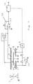
- the arrangement of the electrodes to the running material strip 2 can be seen as a schematic cross-sectional representation, i.e. The material strip 2 runs into and out of the plane of the drawing and is surrounded by the various electrodes over a certain extent.
- transmission electrodes 4, 5, which are shielded by shielding electrodes 7, 8, are arranged below the material strip 2 in the region of its edges.
- An oscillator acts directly on the transmitting electrode 5 and, via an inverting amplifier 14, the transmitting electrode 4.
- the inverting amplifier 14 is an operational amplifier which, in conjunction with the resistors R1, R2, causes a phase shift of 180 °.
- a detector electrode 3 to which a current-voltage converter 10 from an operational amplifier 101 and an output whose impedance Z1 is fed back to the inverting input is connected.
- the output of the current-voltage converter 10 acts on a demodulator 15.
- the area of the detector electrode 3 facing away from the material strip 2 is surrounded by a shielding electrode 6, which is connected to the output of a voltage follower 11, the input of which is connected to the detector electrode 3.
- the oscillator 9 feeds the transmitting electrode 5 and the reversing amplifier 14 the transmitting electrode 4.
- the reversing amplifier 14 causes the same signal amplitude at the transmitting electrode 4 as at the transmitting electrode 5. Only the phase position of the signal at the transmitting electrode 4 is around 180 ° compared to the signal at the Transmitting electrode 5 shifted. Under these conditions, there will be no signal at the detector electrode 3 when the material strip 2 runs through the center of the device, since a capacitive displacement current flows from each of the two transmitter electrodes to the detector electrode and the effect of the two currents at the detector electrode is canceled.
- the capacitive coupling becomes stronger on one edge and weaker on the other edge.
- the capacitive displacement current of one transmitter electrode compared to that of the other transmitter electrode is predominant, so that a differential current arises.
- This differential current now arrives at the negative input of the operational amplifier 101, which is negative-coupled via Z1 .
- the operational amplifier 101 is designed so that it has a very high input impedance. Under this condition, the differential current of the mid-band sensor must flow for the most part by the negative feedback resistor Z1 and the voltage drop at Z1, the output voltage U a of the amplifier determined.
- phase position of the output voltage U a shows which coupling has become stronger and which has become weaker and thus the direction in which the material strip migrates.
- a signal path for the phase position from the oscillator 9 to the demodulator 15 is indicated by dashed lines.
- U e denotes the voltage at the input, U a the voltage at the output and v o the no-load gain of the operational amplifier 101. If the amplifier is designed so that v o is very large, then the voltage at the input of the amplifier is also on the detector electrode 3 is very small and the current-voltage converter 10 overall has a very low input impedance.
- the voltage U a occurring at the output of the current-voltage converter 10 arises in this circuit due to the voltage drop generated by the differential current at Z1 and is proportional to the differential current and the feedback impedance Z1 .
- the AC output voltage of the current-voltage converter 10 is thus a measure of the material band position in the device. It can now be used directly or converted into a proportional DC voltage in a demodulator 15.
- the shielding electrode is used to prevent interference from the environment, which may be caused by persons 1 nearby or by asymmetrically arranged, conductive machine parts, but also by interference fields from other devices in the overall system (welding machines, electrostatic oilers, thyristor-controlled motors, etc.).
- a simple grounding of the shielding electrode 6 would not be optimal because in practice it is not possible to fully force the zero potential at the detector electrode.
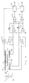
- the width detection electrode is the transmission electrode 3 ', which is fed by the oscillator 9' and from which capacitive displacement currents flow to the two detector electrodes 4 ', 5', which here represent the edge electrodes.
- These two displacement currents are now - each individually - fed to an evaluation circuit with a current-voltage converter 10 'or 12', as described above for the first embodiment.
- the AC voltages at the detector electrodes are kept very low, so that the interference capacitance between the material strip and the detector electrodes remains ineffective.
- the differential amplifier 14 ' forms the difference between the output signals of the current-voltage converters 10', 12 'and the signal thus obtained is then fed back to the demodulator 15'.
- FIG. 3 shows a further embodiment of the first variant, in which the insulation of the active electrodes of the device is monitored. Since the individual electrodes have to be fastened to the device frame by means of insulators, conductive impurities on the surface of these insulators can also impair the function of the device. Insulation monitoring of this kind proves to be particularly advantageous when installing such devices in drying ovens or annealing ovens, since access for maintenance personnel is often very difficult and time-consuming and contamination of the insulators can occur depending on the furnace atmosphere.
- the three electrodes 3 '', 4 ′′ and 5 ′′ connected to a DC voltage source 21 ′′ via resistors R3 ′′, R4 ′′ and R5 ′′.
- the DC voltage at the electrodes can now be monitored by the comparators 18 ′′, 19 ′′ and 20 ′′. If the response thresholds of the comparators and the resistors R3 '', R4 '' and R5 '' are selected correctly, an alarm signal is sent to the outputs of the comparators 18 '', 19 '' and 20 '' before the isolators become dirty the device is impaired.
- the capacitors C1 '', C2 '' and C3 '' decouple the position signal evaluation from the insulation monitoring.
Landscapes
- Physics & Mathematics (AREA)
- General Physics & Mathematics (AREA)
- Engineering & Computer Science (AREA)
- Power Engineering (AREA)
- Measurement Of Length, Angles, Or The Like Using Electric Or Magnetic Means (AREA)
Applications Claiming Priority (2)
| Application Number | Priority Date | Filing Date | Title |
|---|---|---|---|
| DE19511646 | 1995-03-30 | ||
| DE19511646A DE19511646C2 (de) | 1995-03-30 | 1995-03-30 | Vorrichtung zum berührungslosen Erfassen der Lage eines laufenden Materialbandes |
Publications (3)
| Publication Number | Publication Date |
|---|---|
| EP0734986A2 true EP0734986A2 (fr) | 1996-10-02 |
| EP0734986A3 EP0734986A3 (fr) | 1998-01-21 |
| EP0734986B1 EP0734986B1 (fr) | 2001-08-16 |
Family
ID=7758138
Family Applications (1)
| Application Number | Title | Priority Date | Filing Date |
|---|---|---|---|
| EP96104765A Expired - Lifetime EP0734986B1 (fr) | 1995-03-30 | 1996-03-26 | Dispositif pour détecter sans contact la position d'une bande de matériau en mouvement |
Country Status (3)
| Country | Link |
|---|---|
| US (1) | US5767686A (fr) |
| EP (1) | EP0734986B1 (fr) |
| DE (2) | DE19511646C2 (fr) |
Cited By (4)
| Publication number | Priority date | Publication date | Assignee | Title |
|---|---|---|---|---|
| WO1999028702A1 (fr) * | 1997-11-28 | 1999-06-10 | I.E.E. International Electronics & Engineering S.A.R.L. | Mesure de distance capacitive a l'aide d'une electrode de mesure non ideale |
| LU90237B1 (de) * | 1998-04-30 | 1999-11-03 | Iee Sarl | Kapazitive distanzmessung mit einer nicht idealen messelektrode |
| WO2013057159A1 (fr) * | 2011-10-21 | 2013-04-25 | Microchip Technology Germany Ii Gmbh & Co. Kg | Dispositif d'électrode de dispositif de capteur capacitif pour détection de position |
| WO2021123178A1 (fr) | 2019-12-19 | 2021-06-24 | Roche Diagnostics Gmbh | Procédé et système de production d'une pluralité de bandelettes réactives analytiques |
Families Citing this family (17)
| Publication number | Priority date | Publication date | Assignee | Title |
|---|---|---|---|---|
| US6114862A (en) * | 1996-02-14 | 2000-09-05 | Stmicroelectronics, Inc. | Capacitive distance sensor |
| JPH10171030A (ja) * | 1996-12-13 | 1998-06-26 | Noritsu Koki Co Ltd | ピースネガ供給装置 |
| JP3767075B2 (ja) * | 1997-03-24 | 2006-04-19 | ソニー株式会社 | フィルム位置検出装置およびフィルム位置検出方法並びに映像フィルム投影装置 |
| US6091082A (en) | 1998-02-17 | 2000-07-18 | Stmicroelectronics, Inc. | Electrostatic discharge protection for integrated circuit sensor passivation |
| AU5126599A (en) * | 1998-07-24 | 2000-02-14 | Life Measurement Instruments, Inc. | Variable dielectric position transducer and method |
| US6512381B2 (en) | 1999-12-30 | 2003-01-28 | Stmicroelectronics, Inc. | Enhanced fingerprint detection |
| US7239227B1 (en) | 1999-12-30 | 2007-07-03 | Upek, Inc. | Command interface using fingerprint sensor input system |
| US6486680B1 (en) * | 2000-06-13 | 2002-11-26 | The North American Manufacturing Company | Edge detector |
| US6724324B1 (en) * | 2000-08-21 | 2004-04-20 | Delphi Technologies, Inc. | Capacitive proximity sensor |
| NO316796B1 (no) * | 2002-03-01 | 2004-05-10 | Idex Asa | Sensormodul for maling av strukturer i en overflate, saerlig en fingeroverflate |
| JP2004294351A (ja) * | 2003-03-28 | 2004-10-21 | Canon Inc | 電位センサおよび画像形成装置 |
| US20060030182A1 (en) * | 2004-07-29 | 2006-02-09 | Rf Technologies, Inc. | Patient presence monitoring system and method |
| JP4481806B2 (ja) * | 2004-12-03 | 2010-06-16 | アルプス電気株式会社 | 容量検出型センサ |
| US8115497B2 (en) * | 2007-11-13 | 2012-02-14 | Authentec, Inc. | Pixel sensing circuit with common mode cancellation |
| US8554354B1 (en) | 2010-02-12 | 2013-10-08 | The Board Of Regents For Oklahoma State University | Method for adaptive guiding of webs |
| DE102013217485B4 (de) | 2013-09-03 | 2024-09-26 | Körber Technologies Gmbh | Anordnung und Verfahren zur Überprüfung von stabförmigen Artikeln der Tabak verarbeitenden Industrie |
| CN104182745B (zh) * | 2014-08-15 | 2017-09-22 | 深圳市汇顶科技股份有限公司 | 指纹感应信号的处理方法、系统及指纹识别终端 |
Family Cites Families (20)
| Publication number | Priority date | Publication date | Assignee | Title |
|---|---|---|---|---|
| US3341774A (en) * | 1962-07-17 | 1967-09-12 | Comm Res Inc | Capacitance detector having a transmitter connected to one plate and a receiver connected to another plate |
| US3312892A (en) * | 1964-05-04 | 1967-04-04 | Technology Instr Corp Of Calif | Contactless electrical transducer having moving parts |
| US3323699A (en) * | 1965-10-04 | 1967-06-06 | Allegheny Ludlum Steel | Strip centerline sensor and control |
| GB1183974A (en) * | 1967-06-05 | 1970-03-11 | Allegheny Ludlum Steel | Monitoring the Lateral Disposition of a Moving Strip of Material |
| DE1574292C3 (de) * | 1967-06-05 | 1979-04-12 | Allegheny Ludlum Steel Corp., Pittsburgh, Pa. (V.St.A.) | Vorrichtung zum Abtasten der Lage der Seitenkante eines sich bewegenden Materialbandes |
| US3812424A (en) * | 1972-09-27 | 1974-05-21 | Ade Corp | Capacitive wire gauge |
| DE2429109A1 (de) * | 1974-06-18 | 1976-01-08 | Hauni Werke Koerber & Co Kg | Anordnung zum ueberwachen eines streifens aus einem einschlagmaterial der tabakverarbeitenden industrie |
| DE2744785B2 (de) * | 1977-10-05 | 1981-05-21 | Robert 7995 Neukirch Buck | Elektronischer Annäherungsschalter |
| US4322678A (en) * | 1978-10-30 | 1982-03-30 | Capots Larry H | Identification of materials using their complex dielectric response |
| US4584885A (en) * | 1984-01-20 | 1986-04-29 | Harry E. Aine | Capacitive detector for transducers |
| DE3518187C1 (de) * | 1985-05-21 | 1986-07-31 | Fraunhofer-Gesellschaft zur Förderung der angewandten Forschung e.V., 8000 München | Vorrichtung zur berührungslosen Erfassung der Lage eines Objektes, insbesondere der Schwingungen eines vibrierenden Objektes |
| US4719409A (en) * | 1985-10-02 | 1988-01-12 | Mechanical Technology Incorporated | Digital signal output capacitance sensor displacement gauging system |
| GB8718606D0 (en) * | 1987-08-06 | 1987-09-09 | Hiltcroft Packaging Systems Lt | Monitoring apparatus |
| NZ226435A (en) * | 1987-10-02 | 1991-04-26 | Detection Systems Pty Ltd | Capacitance sensor as object detector |
| EP0336022A1 (fr) * | 1988-04-08 | 1989-10-11 | SCHUT'S IM- & EXPORTHANDEL B.V. | Capteur de déplacement capacitif |
| US4893071A (en) * | 1988-05-24 | 1990-01-09 | American Telephone And Telegraph Company, At&T Bell Laboratories | Capacitive incremental position measurement and motion control |
| GB9002701D0 (en) * | 1990-02-07 | 1990-04-04 | Atomic Energy Authority Uk | A gauging system |
| DE4009697A1 (de) * | 1990-03-27 | 1991-10-02 | Fife Gmbh | Vorrichtung zum beruehrungslosen erfassen der lage eines sich bewegenden materialbandes |
| US5309110A (en) * | 1992-03-04 | 1994-05-03 | The Perkin Elmer Corporation | Differential dielectric analyzer |
| GB2295016A (en) * | 1994-11-07 | 1996-05-15 | British Nuclear Fuels Plc | A transducer |
-
1995
- 1995-03-30 DE DE19511646A patent/DE19511646C2/de not_active Revoked
-
1996
- 1996-03-26 EP EP96104765A patent/EP0734986B1/fr not_active Expired - Lifetime
- 1996-03-26 DE DE59607473T patent/DE59607473D1/de not_active Expired - Lifetime
- 1996-03-26 US US08/622,488 patent/US5767686A/en not_active Expired - Lifetime
Cited By (6)
| Publication number | Priority date | Publication date | Assignee | Title |
|---|---|---|---|---|
| WO1999028702A1 (fr) * | 1997-11-28 | 1999-06-10 | I.E.E. International Electronics & Engineering S.A.R.L. | Mesure de distance capacitive a l'aide d'une electrode de mesure non ideale |
| LU90237B1 (de) * | 1998-04-30 | 1999-11-03 | Iee Sarl | Kapazitive distanzmessung mit einer nicht idealen messelektrode |
| WO2013057159A1 (fr) * | 2011-10-21 | 2013-04-25 | Microchip Technology Germany Ii Gmbh & Co. Kg | Dispositif d'électrode de dispositif de capteur capacitif pour détection de position |
| DE102011054690B4 (de) * | 2011-10-21 | 2016-05-12 | Ident Technology Ag | Elektrodeneinrichtung für eine kapazitive Sensoreinrichtung zur Positionserfassung |
| US9442534B2 (en) | 2011-10-21 | 2016-09-13 | Microchip Technology Germany Ii Gmbh & Co. Kg | Electrode device for a capacitive sensor device for position detection |
| WO2021123178A1 (fr) | 2019-12-19 | 2021-06-24 | Roche Diagnostics Gmbh | Procédé et système de production d'une pluralité de bandelettes réactives analytiques |
Also Published As
| Publication number | Publication date |
|---|---|
| US5767686A (en) | 1998-06-16 |
| DE19511646C2 (de) | 1999-01-07 |
| EP0734986A3 (fr) | 1998-01-21 |
| EP0734986B1 (fr) | 2001-08-16 |
| DE59607473D1 (de) | 2001-09-20 |
| DE19511646A1 (de) | 1996-10-02 |
Similar Documents
| Publication | Publication Date | Title |
|---|---|---|
| EP0734986B1 (fr) | Dispositif pour détecter sans contact la position d'une bande de matériau en mouvement | |
| DE69122895T2 (de) | Apparat zur Feststellung der Papierdicke | |
| DE69010568T2 (de) | Keramisches resonanzartiges Elektrostatikfühlergerät. | |
| DE3433148C2 (de) | Anordnung zur Erfassung räumlicher Inhomogenitäten in einem Dielektrikum | |
| DE69331895T2 (de) | Magnetoresistiver Magnetfeldsensor mit sehr langem Wirkbereich | |
| DE4009697C2 (fr) | ||
| DE102008020153A1 (de) | Winkelerfassungsvorrichtung | |
| DE68912491T2 (de) | Magnetlager. | |
| DE2344008B2 (de) | Meßgerät zum Messen von Veränderungen der physikalischen Eigenschaften eines magnetisch oder elektrisch leitenden Untersuchungsobjekts | |
| DE2459155C3 (de) | Schaltung zur Feststellung von Überströmen | |
| DE2623698A1 (de) | Verfahren und vorrichtung zur feuchtemessung von flaechengebilden, insbesondere textilbahnen | |
| DE19733904C2 (de) | Magnetische Erfassungsvorichtung | |
| EP3764054B1 (fr) | Agencement de capteur permettant de détecter une déviation d'une fil électrode | |
| DE10027507C1 (de) | Schaltungsanordnung zur Erfassung von Kapazitätsänderungen | |
| DE1499064A1 (de) | Verfahren und Vorrichtung zur Bestimmung der Bahnlage | |
| DE4413840C2 (de) | Vorrichtung zur berührungslosen Messung an einem Objekt | |
| EP0101923B1 (fr) | Contrôle de courroies transporteuses pour déceler des fissures longitudinales | |
| DE19850290C2 (de) | Schaltungsanordnung zur linearen kapazitiven Messung | |
| DE2714142A1 (de) | Einrichtung zur messung eines magnetflusses | |
| DE2420120A1 (de) | Messvorrichtung | |
| DE4104714C2 (de) | Schaltungsanordnung zur Verarbeitung von elektrischen Signalen | |
| EP0503501B1 (fr) | Appareil pour déterminer l'écartement entre deux rouleaux | |
| DE202007009794U1 (de) | Sensor zur Erfassung eines elektrischen Potentials auf der Haut | |
| EP0974812B1 (fr) | Dispositif pour détecter des étiquettes sur un support | |
| AT504403B1 (de) | Verfahren und vorrichtung zum messen zweier teilkapazitäten |
Legal Events
| Date | Code | Title | Description |
|---|---|---|---|
| PUAI | Public reference made under article 153(3) epc to a published international application that has entered the european phase |
Free format text: ORIGINAL CODE: 0009012 |
|
| AK | Designated contracting states |
Kind code of ref document: A2 Designated state(s): BE DE ES FR GB IT LU NL SE |
|
| PUAL | Search report despatched |
Free format text: ORIGINAL CODE: 0009013 |
|
| AK | Designated contracting states |
Kind code of ref document: A3 Designated state(s): BE DE ES FR GB IT LU NL SE |
|
| 17P | Request for examination filed |
Effective date: 19980425 |
|
| 17Q | First examination report despatched |
Effective date: 19990831 |
|
| GRAG | Despatch of communication of intention to grant |
Free format text: ORIGINAL CODE: EPIDOS AGRA |
|
| GRAG | Despatch of communication of intention to grant |
Free format text: ORIGINAL CODE: EPIDOS AGRA |
|
| GRAG | Despatch of communication of intention to grant |
Free format text: ORIGINAL CODE: EPIDOS AGRA |
|
| GRAH | Despatch of communication of intention to grant a patent |
Free format text: ORIGINAL CODE: EPIDOS IGRA |
|
| GRAH | Despatch of communication of intention to grant a patent |
Free format text: ORIGINAL CODE: EPIDOS IGRA |
|
| GRAA | (expected) grant |
Free format text: ORIGINAL CODE: 0009210 |
|
| AK | Designated contracting states |
Kind code of ref document: B1 Designated state(s): BE DE ES FR GB IT LU NL SE |
|
| PG25 | Lapsed in a contracting state [announced via postgrant information from national office to epo] |
Ref country code: NL Free format text: LAPSE BECAUSE OF FAILURE TO SUBMIT A TRANSLATION OF THE DESCRIPTION OR TO PAY THE FEE WITHIN THE PRESCRIBED TIME-LIMIT Effective date: 20010816 |
|
| RAP2 | Party data changed (patent owner data changed or rights of a patent transferred) |
Owner name: FIFE-TIDLAND GMBH |
|
| REF | Corresponds to: |
Ref document number: 59607473 Country of ref document: DE Date of ref document: 20010920 |
|
| NLT2 | Nl: modifications (of names), taken from the european patent patent bulletin |
Owner name: FIFE-TIDLAND GMBH |
|
| ET | Fr: translation filed | ||
| PG25 | Lapsed in a contracting state [announced via postgrant information from national office to epo] |
Ref country code: SE Free format text: LAPSE BECAUSE OF FAILURE TO SUBMIT A TRANSLATION OF THE DESCRIPTION OR TO PAY THE FEE WITHIN THE PRESCRIBED TIME-LIMIT Effective date: 20011116 |
|
| GBT | Gb: translation of ep patent filed (gb section 77(6)(a)/1977) |
Effective date: 20011025 |
|
| REG | Reference to a national code |
Ref country code: GB Ref legal event code: IF02 |
|
| NLV1 | Nl: lapsed or annulled due to failure to fulfill the requirements of art. 29p and 29m of the patents act | ||
| PG25 | Lapsed in a contracting state [announced via postgrant information from national office to epo] |
Ref country code: ES Free format text: LAPSE BECAUSE OF FAILURE TO SUBMIT A TRANSLATION OF THE DESCRIPTION OR TO PAY THE FEE WITHIN THE PRESCRIBED TIME-LIMIT Effective date: 20020228 |
|
| PG25 | Lapsed in a contracting state [announced via postgrant information from national office to epo] |
Ref country code: LU Free format text: LAPSE BECAUSE OF NON-PAYMENT OF DUE FEES Effective date: 20020326 |
|
| PG25 | Lapsed in a contracting state [announced via postgrant information from national office to epo] |
Ref country code: BE Free format text: LAPSE BECAUSE OF NON-PAYMENT OF DUE FEES Effective date: 20020331 |
|
| PLBQ | Unpublished change to opponent data |
Free format text: ORIGINAL CODE: EPIDOS OPPO |
|
| PLBI | Opposition filed |
Free format text: ORIGINAL CODE: 0009260 |
|
| PLBF | Reply of patent proprietor to notice(s) of opposition |
Free format text: ORIGINAL CODE: EPIDOS OBSO |
|
| 26 | Opposition filed |
Opponent name: FIRMA ELEKTRO MECHANIK GMBH Effective date: 20020516 |
|
| PLBF | Reply of patent proprietor to notice(s) of opposition |
Free format text: ORIGINAL CODE: EPIDOS OBSO |
|
| BERE | Be: lapsed |
Owner name: *FIFE G.M.B.H. Effective date: 20020331 |
|
| PLBP | Opposition withdrawn |
Free format text: ORIGINAL CODE: 0009264 |
|
| PLBL | Opposition procedure terminated |
Free format text: ORIGINAL CODE: EPIDOS OPPC |
|
| PLBM | Termination of opposition procedure: date of legal effect published |
Free format text: ORIGINAL CODE: 0009276 |
|
| STAA | Information on the status of an ep patent application or granted ep patent |
Free format text: STATUS: OPPOSITION PROCEDURE CLOSED |
|
| 27C | Opposition proceedings terminated |
Effective date: 20030411 |
|
| PLAB | Opposition data, opponent's data or that of the opponent's representative modified |
Free format text: ORIGINAL CODE: 0009299OPPO |
|
| REG | Reference to a national code |
Ref country code: DE Ref legal event code: R082 Ref document number: 59607473 Country of ref document: DE Representative=s name: MEHLER ACHLER PATENTANWAELTE PARTNERSCHAFT MBB, DE Ref country code: DE Ref legal event code: R082 Ref document number: 59607473 Country of ref document: DE Representative=s name: MEHLER ACHLER PATENTANWAELTE, DE |
|
| REG | Reference to a national code |
Ref country code: FR Ref legal event code: PLFP Year of fee payment: 20 |
|
| PGFP | Annual fee paid to national office [announced via postgrant information from national office to epo] |
Ref country code: IT Payment date: 20150326 Year of fee payment: 20 Ref country code: DE Payment date: 20150318 Year of fee payment: 20 |
|
| PGFP | Annual fee paid to national office [announced via postgrant information from national office to epo] |
Ref country code: GB Payment date: 20150324 Year of fee payment: 20 Ref country code: FR Payment date: 20150319 Year of fee payment: 20 |
|
| REG | Reference to a national code |
Ref country code: DE Ref legal event code: R071 Ref document number: 59607473 Country of ref document: DE |
|
| REG | Reference to a national code |
Ref country code: GB Ref legal event code: PE20 Expiry date: 20160325 |
|
| PG25 | Lapsed in a contracting state [announced via postgrant information from national office to epo] |
Ref country code: GB Free format text: LAPSE BECAUSE OF EXPIRATION OF PROTECTION Effective date: 20160325 |