EP0735541B1 - Leseverfahren eines ferroelektrischen Speichers unter Verwendung von unterschiedlichen Lese- und Schreibespannungen - Google Patents
Leseverfahren eines ferroelektrischen Speichers unter Verwendung von unterschiedlichen Lese- und Schreibespannungen Download PDFInfo
- Publication number
- EP0735541B1 EP0735541B1 EP96301669A EP96301669A EP0735541B1 EP 0735541 B1 EP0735541 B1 EP 0735541B1 EP 96301669 A EP96301669 A EP 96301669A EP 96301669 A EP96301669 A EP 96301669A EP 0735541 B1 EP0735541 B1 EP 0735541B1
- Authority
- EP
- European Patent Office
- Prior art keywords
- voltage
- ferroelectric
- charge
- pulse
- plate line
- Prior art date
- Legal status (The legal status is an assumption and is not a legal conclusion. Google has not performed a legal analysis and makes no representation as to the accuracy of the status listed.)
- Expired - Lifetime
Links
- 238000000034 method Methods 0.000 title claims description 28
- 239000003990 capacitor Substances 0.000 claims description 65
- 230000010287 polarization Effects 0.000 claims description 14
- 238000010586 diagram Methods 0.000 description 24
- 239000000463 material Substances 0.000 description 13
- 230000014759 maintenance of location Effects 0.000 description 8
- 229920006395 saturated elastomer Polymers 0.000 description 8
- 239000000872 buffer Substances 0.000 description 6
- 229910052451 lead zirconate titanate Inorganic materials 0.000 description 6
- 239000004020 conductor Substances 0.000 description 3
- 230000003292 diminished effect Effects 0.000 description 3
- 230000004044 response Effects 0.000 description 3
- 230000008901 benefit Effects 0.000 description 2
- 239000003989 dielectric material Substances 0.000 description 2
- 230000009977 dual effect Effects 0.000 description 2
- 230000006870 function Effects 0.000 description 2
- 238000001208 nuclear magnetic resonance pulse sequence Methods 0.000 description 2
- 238000009738 saturating Methods 0.000 description 2
- 230000007704 transition Effects 0.000 description 2
- 238000010420 art technique Methods 0.000 description 1
- 230000006399 behavior Effects 0.000 description 1
- 229910002115 bismuth titanate Inorganic materials 0.000 description 1
- 230000000295 complement effect Effects 0.000 description 1
- 238000003708 edge detection Methods 0.000 description 1
- 230000000694 effects Effects 0.000 description 1
- 230000006872 improvement Effects 0.000 description 1
- 230000000977 initiatory effect Effects 0.000 description 1
- 150000002500 ions Chemical class 0.000 description 1
- 229910052746 lanthanum Inorganic materials 0.000 description 1
- FZLIPJUXYLNCLC-UHFFFAOYSA-N lanthanum atom Chemical compound [La] FZLIPJUXYLNCLC-UHFFFAOYSA-N 0.000 description 1
- HFGPZNIAWCZYJU-UHFFFAOYSA-N lead zirconate titanate Chemical compound [O-2].[O-2].[O-2].[O-2].[O-2].[Ti+4].[Zr+4].[Pb+2] HFGPZNIAWCZYJU-UHFFFAOYSA-N 0.000 description 1
- 230000007246 mechanism Effects 0.000 description 1
- 230000004048 modification Effects 0.000 description 1
- 238000012986 modification Methods 0.000 description 1
- 230000001105 regulatory effect Effects 0.000 description 1
- 230000000717 retained effect Effects 0.000 description 1
Images


Classifications
-
- G—PHYSICS
- G11—INFORMATION STORAGE
- G11C—STATIC STORES
- G11C11/00—Digital stores characterised by the use of particular electric or magnetic storage elements; Storage elements therefor
- G11C11/21—Digital stores characterised by the use of particular electric or magnetic storage elements; Storage elements therefor using electric elements
- G11C11/22—Digital stores characterised by the use of particular electric or magnetic storage elements; Storage elements therefor using electric elements using ferroelectric elements
Definitions
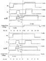
- FIGS. 2A-D The operation of a ferroelectric capacitor such as ferroelectric capacitor 16 or 18 in memory cell 10 is illustrated in FIGS. 2A-D by way of a series of hysteresis loop diagrams 28A-D and corresponding voltage waveform diagrams 38A-D.
- Hysteresis loop diagrams 28A-D show the electrical performance of a ferroelectric capacitor, wherein the x-axis represents the voltage applied across the capacitor, and the y-axis represents the charge evolved by the ferroelectric capacitor in response to the applied voltage.
- Corresponding waveform diagrams 38A-D are a series of two positive voltage pulses and two negative voltage pulses that are applied across a ferroelectric capacitor in a known sequence that illustrates the complete electrical behavior of a ferroelectric capacitor.
- Hysteresis loop diagram 28A of FIG. 2A includes a hysteresis loop 30 and an initial operating point 32.
- Operating point 32 represents a ferroelectric capacitor having, by convention, an "up" polarization state, but with no applied voltage across the capacitor.
- the initial operating point 32 is achieved by a previous application and removal of a negative applied voltage across the capacitor.
- the operating point of the ferroelectric capacitor moves from operating point 32 to operating point 34 upon the application of a positive voltage pulse.
- Operating point 34 represents a fully saturated ferroelectric capacitor operating condition, i.e. further increases in applied voltage do not yield an appreciable amount of extra charge.
- the amount of charge evolved from operating point 32 to operating point 34 (the difference in the y-axis values) is designated "P".
- a voltage pulse of about four volts is used.
- a four volt pulse ensures that, while the ferroelectric material is not completely saturated, a sufficient quantity of charge is evolved that can be detected by conventional memory sense circuitry.
- the total cycle time depicted is about 250 nanoseconds, with the write pulse in FIG. 4A and the restore pulse in FIG. 4B having a pulse width of about 20 nanoseconds.
- the pulsewidth of the initial read pulse is about the same as the write and restore pulse.
Landscapes
- Engineering & Computer Science (AREA)
- Computer Hardware Design (AREA)
- Dram (AREA)
Claims (20)
- Verfahren zum Betreiben einer permanenten, ferroelektrischen Speicherzelle mit einem polarisierten ferroelektrischen Kondensator, wobei das Verfahren folgende Schritte umfaßt:während eines Lesevorgangs, das Lesen und Wiederherstellen eines ersten Polarisierungszustands des ferroelektrischen Kondensators bei einer Spannung, die nicht ausreicht, um den ferroelektrischen Kondensator vollständig zu sättigen, aber ausreicht, um eine erfaßbare Ladungsmenge freizusetzen, die dem ersten Polarisierungszustand entspricht; undwährend eines Schreibvorgangs, das Schreiben eines zweiten Polarisierungszustandes in den ferroelektrischen Kondensator bei einer Spannung, die ausreicht, um den ferroelektrischen Kondensator vollständig zu sättigen.
- Verfahren nach Anspruch 1, bei dem der Lese- und Wiederherstellschritt folgende Schritte umfaßt:Anlegen eines ersten Spannungsimpulses am ferroelektrischen Kondensator;Erfassen der Ladung am ferroelektrischen Kondensator; undAnlegen eines zweiten Spannungsimpulses am ferroelektrischen Kondensator, wobei die Höhe der ersten und zweiten Spannungsimpulse nicht ausreicht, um den ferroelektrischen Kondensator vollständig zu sättigen.
- Verfahren nach Anspruch 1, bei dem der Schreibschritt den Schritt umfaßt, einen Spannungsimpuls am ferroelektrischen Kondensator anzulegen, der ausreicht um diesen vollständig zu sättigen.
- Verfahren zum Betrieb einer permanenten, ferroelektrischen Speicherzelle mit einem Paar polarisierter ferroelektrischer Kondensatoren (16, 18), einer Unterscheidungsbit-Leitung (24, 26), einer Wortleitung (20) und einer Plattenleitung (22), wobei das Verfahren die Schritte umfaßt:im Lesebetrieb,Anlegen eines ersten Spannungsimpulses an der Plattenleitung, der nicht ausreicht, um die ferroelektrischen Kondensatoren (16, 18) vollständig zu sättigen, aber ausreicht, um eine erfaßbare Ladungsmenge an die Unterscheidungs-Bitleitung (24, 26) abzugeben, die einem ersten Datenzustand entspricht,Abbauen der Ladung an der Unterscheidungs-Bitleitung (24, 26), undAnlegen eines zweiten Spannungsimpulses an der Plattenleitung (22),der nicht ausreicht, um die ferroelektrischen Kondensatoren (16, 18) vollständig zu sättigen, der aber ausreicht, um den ersten Datenzustand wiederherzustellen;im Schreibbetrieb,Anlegen eines ersten Spannungsimpulses an der Plattenleitung (22), der nicht ausreicht, um die ferroelektrischen Kondensatoren (16, 18) vollständig zu sättigen,Aufbringen einer Ladung, die einem angestrebten, zweiten Datenzustand entspricht, auf die Unterscheidungs-Bitleitung (24, 26)Abbauen der Ladung an der Unterscheidungs-Bitleitung (24, 26), undAnlegen eines zweiten Spannungsimpulses an der Plattenleitung (22), der ausreicht, um die ferroelektrischen Kondensatoren (16, 18) vollständig zu sättigen, um einen zweiten Datenzustand einzurichten.
- Verfahren nach Anspruch 4, bei dem die Pulsschritte, die bei einer Spannung ausgeführt werden, die nicht ausreicht, um die ferroelektrischen Kondensatoren (16, 18) vollständig zu sättigen, jeweils das Pulsen der Plattenleitung (22) mit einer Spannung von etwa 4 Volt umfassen.
- Verfahren nach Anspruch 4, bei dem der Pulsschritt, der bei einer Spannung durchgeführt wird, die ausreicht, um die ferroelektrischen Kondensatoren (16, 18) vollständig zu sättigen, das Pulsen der Plattenleitung mit einer Spannung von etwa 6 bis 7 Volt umfaßt.
- Verfahren nach Anspruch 4, ferner das Pulsen der Wortleitung 20 mit einem Spannungsimpuls umfassend, der während des Schreibvorgangs einen ersten, niedrigen Spannungsabschnitt und einen zweiten, höheren Spannungsabschnitt hat.
- Verfahren nach Anspruch 7, bei dem der erste niedrige Spannungsabschnitt während des ersten Plattenleitungs-Spannungsimpulses auftritt, und der zweite, höhere Spannungsabschnitt während des zweiten Plattenleitungs-Spannungsimpulses auftritt.
- Verfahren nach Anspruch 4, ferner den Schritt des Pulsens der Wortleitung 20 während des Schreibvorgangs umfassend, wobei der Spannungsimpuls einen 4 Volt-Abschnitt und einen 6 Volt-Abschnitt hat.
- Verfahren nach Anspruch 4, in dem :der Abbauschritt während des Lesevorgangs das Konvertieren der Unterscheidungsbit-Leitungsladung in ein erstes logisches Unterscheidungssignal niedriger Spannung umfaßt; undder Abbauschritt während des Schreibvorgangs das Konvertieren der Unterscheidungsbit-Leitungsladung in ein logisches Unterscheidungssignal höherer Spannung umfaßt.
- Verfahren nach Anspruch 10, bei dem der Abbauschritt während des Lesevorgangs das Konvertieren der Unterscheidungsbit-Leitungsladung in ein logisches 4 Volt-Unterscheidungssignal umfaßt.
- Verfahren nach Anspruch 10, bei dem der Abbauschritt während des Schreibvorgangs das Umwandeln an der Unterscheidungsbit-Leitungsladung in ein logisches 6 - 7 Volt-Unterscheidungssignal umfaßt.
- Ferroelektrischer Speicher, umfassend:eine ferroelektrische Speicherzelle (62), die einen ferroelektrischen Kondensator, eine Wortleitung, eine Plattenleitung und eine Bitleitung enthält; undeine Einrichtung (64), um wahlweise eine Erdungsspannung, eine erste, niedrige Spannung und eine zweite, hohe Spannung an die Wort- und Plattenleitungen anzulegen, wobei die erste, niedrige Spannung nicht ausreicht, um den ferroelektrischen Kondensator vollständig zu sättigen und die zweite, hohe Spannung ausreicht, um den ferroelektrischen Kondensator vollständig zu sättigen.
- Ferroelektrischer Speicher nach Anspruch 13, in dem die Einrichtung (64), um wahlweise eine Erdungsspannung, eine erste, niedrige Spannung und eine zweite, hohe Spannung an den Wort- und Plattenleitungen anzulegen, umfaßt:eine Einrichtung, um wahlweise entweder einen niedrigen Spannungsimpuls oder einen Impuls mit einem ersten, niedrigen Spannungsabschnitt und einen zweiten, hohen Spannungsabschnitt an die Wortleitung zu liefern; undeine Einrichtung, um wahlweise entweder erste und zweite niedrige Spannungsimpulse oder einen ersten, niedrigen Spannungsimpuls und einen zweiten, hohen Spannungsimpuls an die Plattenleitung zu liefern.
- Ferroelektrischer Speicher nach Anspruch 13, bei dem die erste niedrige Spannung etwa 4 Volt und die zweite hohe Spannung etwa 6 bis 7 Volt beträgt.
- Ferroelektrischer Speicher nach Anspruch 13, bei dem die Einrichtung (64), um wahlweise eine Erdungsspannung, eine erste, niedrige Spannung und eine zweite, hohe Spannung anzulegen, folgendes umfaßt:einen Wortleitungstreiber, der an die Wortleitung gekoppelt ist;einen Plattenleitungstreiber, der an die Plattenleitung gekoppelt ist; undeine Einrichtung 68, um eine wählbare Versorgungsspannung an die Wort- und Plattenleitungstreiber zu liefern.
- Ferroelektrischer Speicher nach Anspruch 16, bei dem die Einrichtung (68A) zum Liefern einer wählbaren Versorgungsspannung an die Wort- und Plattenleitungstreiber die Kombination aus einer Ladungspumpe (78) und einem Spannungsregulierer (76) umfaßt.
- Ferroelektrischer Speicher nach Anspruch 16, bei dem die Einrichtung zum Liefern einer wählbaren Versorgungsspannung an die Wort- und Plattenleitungstreiber folgendes umfaßt:einen Spannungsregulierer (76) mit einem Eingang zum Aufnehmen einer Versorgungsspannung und einem Ausgang;eine Ladungspumpe (78) mit einem Eingang zum Aufnehmen einer Versorgungsspannung und einem Ausgang; undeinen Multiplexer (80) mit ersten und zweiten Eingängen, die an die Ausgänge des Spannungsregulierers und der Ladungspumpe gekoppelt sind, einem dritten Eingang, der ein Steuersignal empfängt, und einem Ausgang zum Liefern einer wählbaren Versorgungsspannung.
- Ferroelektrischer Speicher nach Anspruch 16, bei dem die Einrichtung zum Liefern einer wählbaren Versorgungsspannung an die Wort- und Plattenleitungstreiber folgendes umfaßt:eine Ladungspumpe (78) mit einem Eingang zum Aufnehmen einer Versorgungsspannung und einem Ausgang; undeinen Multiplexer (80) mit ersten und zweiten Eingängen zum Aufnehmen der Versorgungsspannung und der Ausgabe der Ladungspumpe, einem dritten Eingang, der ein Steuersignal empfängt, und einem Ausgang zum Liefern der wählbaren Versorgungsspannung.
- Ferroelektrischer Speicher nach Anspruch 13, bei dem die Speicherzelle Teil eines Feldes (62) solcher Zellen ist, die in Reihen und Spalten angeordnet sind.
Applications Claiming Priority (2)
| Application Number | Priority Date | Filing Date | Title |
|---|---|---|---|
| US413083 | 1995-03-29 | ||
| US08/413,083 US5532953A (en) | 1995-03-29 | 1995-03-29 | Ferroelectric memory sensing method using distinct read and write voltages |
Publications (3)
| Publication Number | Publication Date |
|---|---|
| EP0735541A2 EP0735541A2 (de) | 1996-10-02 |
| EP0735541A3 EP0735541A3 (de) | 1998-07-22 |
| EP0735541B1 true EP0735541B1 (de) | 2001-06-13 |
Family
ID=23635749
Family Applications (1)
| Application Number | Title | Priority Date | Filing Date |
|---|---|---|---|
| EP96301669A Expired - Lifetime EP0735541B1 (de) | 1995-03-29 | 1996-03-12 | Leseverfahren eines ferroelektrischen Speichers unter Verwendung von unterschiedlichen Lese- und Schreibespannungen |
Country Status (4)
| Country | Link |
|---|---|
| US (1) | US5532953A (de) |
| EP (1) | EP0735541B1 (de) |
| JP (1) | JP3200009B2 (de) |
| DE (1) | DE69613266T2 (de) |
Families Citing this family (39)
| Publication number | Priority date | Publication date | Assignee | Title |
|---|---|---|---|---|
| KR100333153B1 (ko) | 1993-09-07 | 2002-12-05 | 가부시키가이샤 한도오따이 에네루기 켄큐쇼 | 반도체장치제작방법 |
| JPH07109573A (ja) * | 1993-10-12 | 1995-04-25 | Semiconductor Energy Lab Co Ltd | ガラス基板および加熱処理方法 |
| US5682344A (en) * | 1995-09-11 | 1997-10-28 | Micron Technology, Inc. | Destructive read protection using address blocking technique |
| TW322578B (de) * | 1996-03-18 | 1997-12-11 | Matsushita Electron Co Ltd | |
| US5703804A (en) * | 1996-09-26 | 1997-12-30 | Sharp Kabushiki K.K. | Semiconductor memory device |
| US5990513A (en) | 1996-10-08 | 1999-11-23 | Ramtron International Corporation | Yield enhancement technique for integrated circuit processing to reduce effects of undesired dielectric moisture retention and subsequent hydrogen out-diffusion |
| KR100206713B1 (ko) * | 1996-10-09 | 1999-07-01 | 윤종용 | 강유전체 메모리 장치에서의 비파괴적 억세싱 방법 및 그 억세싱 회로 |
| KR100248355B1 (ko) * | 1997-04-09 | 2000-03-15 | 김영환 | 반도체 메모리 소자의 가변 비교전압 발생장치 |
| US6118688A (en) * | 1997-06-05 | 2000-09-12 | Matsushita Electronics Corporation | Ferroelectric memory device and method for driving it |
| WO1999000798A1 (fr) * | 1997-06-27 | 1999-01-07 | Matsushita Electronics Corporation | Dispositif a memoire ferroelectrique et son procede de commande |
| KR100297874B1 (ko) | 1997-09-08 | 2001-10-24 | 윤종용 | 강유전체랜덤액세스메모리장치 |
| KR100252052B1 (ko) * | 1997-12-03 | 2000-04-15 | 윤종용 | 셀 테스트 패턴을 사용하여 강유전체 기억소자의 특성을 평가하는 방법 |
| US6157979A (en) * | 1998-03-14 | 2000-12-05 | Advanced Technology Materials, Inc. | Programmable controlling device with non-volatile ferroelectric state-machines for restarting processor when power is restored with execution states retained in said non-volatile state-machines on power down |
| US6242299B1 (en) | 1999-04-01 | 2001-06-05 | Ramtron International Corporation | Barrier layer to protect a ferroelectric capacitor after contact has been made to the capacitor electrode |
| US6219270B1 (en) * | 1999-05-24 | 2001-04-17 | U.S. Philips Corporation | Integrated circuit having dynamic memory with boosted plateline |
| JP2001093286A (ja) * | 1999-09-21 | 2001-04-06 | Nec Corp | 強誘電体記憶装置及びその製造方法 |
| JP3916837B2 (ja) * | 2000-03-10 | 2007-05-23 | 株式会社東芝 | 強誘電体メモリ |
| KR100382546B1 (ko) * | 2000-12-04 | 2003-05-09 | 주식회사 하이닉스반도체 | 불휘발성 강유전체 메모리 장치 및 그를 이용한 불량셀검출방법 |
| JP2002269972A (ja) * | 2000-12-27 | 2002-09-20 | Seiko Epson Corp | 強誘電体メモリ装置および強誘電体キャパシタからなるメモリセルに対する動作方法 |
| US6535446B2 (en) | 2001-05-24 | 2003-03-18 | Ramtron International Corporation | Two stage low voltage ferroelectric boost circuit |
| US6430093B1 (en) | 2001-05-24 | 2002-08-06 | Ramtron International Corporation | CMOS boosting circuit utilizing ferroelectric capacitors |
| JP4024166B2 (ja) * | 2002-03-20 | 2007-12-19 | 三洋電機株式会社 | 強誘電体メモリ |
| JP3650077B2 (ja) * | 2002-03-29 | 2005-05-18 | 沖電気工業株式会社 | 半導体記憶装置 |
| US6741504B2 (en) * | 2002-07-19 | 2004-05-25 | Micron Technology, Inc. | Method and apparatus for reducing gate-induced diode leakage in semiconductor devices |
| KR100469153B1 (ko) * | 2002-08-30 | 2005-02-02 | 주식회사 하이닉스반도체 | 강유전체 메모리 장치 |
| KR100492800B1 (ko) * | 2002-11-12 | 2005-06-07 | 주식회사 하이닉스반도체 | 불휘발성 강유전체 메모리 제어 장치 |
| JP2004220705A (ja) * | 2003-01-15 | 2004-08-05 | Seiko Epson Corp | 強誘電体記憶装置 |
| JP4041054B2 (ja) * | 2003-11-06 | 2008-01-30 | 株式会社東芝 | 半導体集積回路装置 |
| JP4511377B2 (ja) * | 2005-01-28 | 2010-07-28 | パナソニック株式会社 | 強誘電体記憶装置 |
| JP4667888B2 (ja) * | 2005-02-01 | 2011-04-13 | パナソニック株式会社 | 半導体記憶装置 |
| KR100694406B1 (ko) * | 2005-04-21 | 2007-03-12 | 주식회사 하이닉스반도체 | 불량 셀 처리 회로를 포함하는 불휘발성 강유전체 메모리장치 및 제어 방법 |
| US7609559B2 (en) * | 2007-01-12 | 2009-10-27 | Micron Technology, Inc. | Word line drivers having a low pass filter circuit in non-volatile memory device |
| US9846664B2 (en) | 2010-07-09 | 2017-12-19 | Cypress Semiconductor Corporation | RFID interface and interrupt |
| US9092582B2 (en) | 2010-07-09 | 2015-07-28 | Cypress Semiconductor Corporation | Low power, low pin count interface for an RFID transponder |
| US8723654B2 (en) | 2010-07-09 | 2014-05-13 | Cypress Semiconductor Corporation | Interrupt generation and acknowledgment for RFID |
| US8842460B2 (en) | 2012-11-26 | 2014-09-23 | Cypress Semiconductor Corporation | Method for improving data retention in a 2T/2C ferroelectric memory |
| US9361972B1 (en) * | 2015-03-20 | 2016-06-07 | Intel Corporation | Charge level maintenance in a memory |
| US9697882B1 (en) * | 2016-08-30 | 2017-07-04 | Radiant Technologies, Inc. | Analog ferroelectric memory with improved temperature range |
| WO2022064303A1 (ja) * | 2020-09-22 | 2022-03-31 | 株式会社半導体エネルギー研究所 | 半導体装置、及び電子機器 |
Family Cites Families (3)
| Publication number | Priority date | Publication date | Assignee | Title |
|---|---|---|---|---|
| US5270967A (en) * | 1991-01-16 | 1993-12-14 | National Semiconductor Corporation | Refreshing ferroelectric capacitors |
| FR2688090B1 (fr) * | 1992-02-27 | 1994-04-08 | Commissariat A Energie Atomique | Cellule memoire non volatile du type metal-ferroelectrique semi-conducteur. |
| US5309391A (en) * | 1992-10-02 | 1994-05-03 | National Semiconductor Corporation | Symmetrical polarization enhancement in a ferroelectric memory cell |
-
1995
- 1995-03-29 US US08/413,083 patent/US5532953A/en not_active Expired - Fee Related
-
1996
- 1996-03-12 DE DE69613266T patent/DE69613266T2/de not_active Expired - Fee Related
- 1996-03-12 EP EP96301669A patent/EP0735541B1/de not_active Expired - Lifetime
- 1996-03-29 JP JP07659496A patent/JP3200009B2/ja not_active Expired - Fee Related
Also Published As
| Publication number | Publication date |
|---|---|
| DE69613266T2 (de) | 2001-09-20 |
| EP0735541A2 (de) | 1996-10-02 |
| JP3200009B2 (ja) | 2001-08-20 |
| DE69613266D1 (de) | 2001-07-19 |
| JPH08273375A (ja) | 1996-10-18 |
| EP0735541A3 (de) | 1998-07-22 |
| US5532953A (en) | 1996-07-02 |
Similar Documents
| Publication | Publication Date | Title |
|---|---|---|
| EP0735541B1 (de) | Leseverfahren eines ferroelektrischen Speichers unter Verwendung von unterschiedlichen Lese- und Schreibespannungen | |
| US5847989A (en) | Ferroelectric memory using non-remnant reference circuit | |
| US5638318A (en) | Ferroelectric memory using ferroelectric reference cells | |
| CN110741437B (zh) | 2t1c铁电随机存取存储器单元 | |
| US5835400A (en) | Ferroelectric memory devices having nondestructive read capability and methods of operating same | |
| US5999439A (en) | Ferroelectric memory using ferroelectric reference cells | |
| US5373463A (en) | Ferroelectric nonvolatile random access memory having drive line segments | |
| US6906944B2 (en) | Ferroelectric memory | |
| US6487104B2 (en) | Semiconductor memory device | |
| US6704218B2 (en) | FeRAM with a single access/multiple-comparison operation | |
| US6522567B2 (en) | Semiconductor memory device and semiconductor integrated device using the same | |
| US5907861A (en) | Destructive read protection using address blocking technique | |
| US7313011B2 (en) | Ferroelectric memory devices having a plate line control circuit | |
| US6522568B1 (en) | Ferroelectric memory and method for reading the same | |
| US20050259461A1 (en) | Ferroelectric memory and method for reading data from the ferroelectric memory | |
| JP2001338499A (ja) | 強誘電体型記憶装置およびそのテスト方法 | |
| US5835399A (en) | Imprint compensation circuit for use in ferroelectric semiconductor memory device | |
| US6646904B2 (en) | Ferroelectric memory and method of reading the same | |
| US5892705A (en) | Apparatus for maintaining non-volatility in ferroelectric ramdom access memory and method therefor | |
| US6438020B1 (en) | Ferroelectric memory device having an internal supply voltage, which is lower than the external supply voltage, supplied to the memory cells | |
| KR100462085B1 (ko) | 반도체 기억 회로 | |
| JP3717097B2 (ja) | 強誘電体メモリ | |
| US7009864B2 (en) | Zero cancellation scheme to reduce plateline voltage in ferroelectric memory | |
| US6310797B1 (en) | Drive method for FeRAM memory cell and drive device for the memory cell | |
| DE102005006343B4 (de) | Integrierter Halbleiterspeicher mit taktsynchroner Zugriffssteuerung |
Legal Events
| Date | Code | Title | Description |
|---|---|---|---|
| PUAI | Public reference made under article 153(3) epc to a published international application that has entered the european phase |
Free format text: ORIGINAL CODE: 0009012 |
|
| AK | Designated contracting states |
Kind code of ref document: A2 Designated state(s): DE GB |
|
| PUAL | Search report despatched |
Free format text: ORIGINAL CODE: 0009013 |
|
| AK | Designated contracting states |
Kind code of ref document: A3 Designated state(s): DE GB |
|
| 17P | Request for examination filed |
Effective date: 19980910 |
|
| 111Z | Information provided on other rights and legal means of execution |
Free format text: 19990412 DE GB |
|
| 17Q | First examination report despatched |
Effective date: 19991105 |
|
| GRAG | Despatch of communication of intention to grant |
Free format text: ORIGINAL CODE: EPIDOS AGRA |
|
| GRAG | Despatch of communication of intention to grant |
Free format text: ORIGINAL CODE: EPIDOS AGRA |
|
| GRAH | Despatch of communication of intention to grant a patent |
Free format text: ORIGINAL CODE: EPIDOS IGRA |
|
| GRAH | Despatch of communication of intention to grant a patent |
Free format text: ORIGINAL CODE: EPIDOS IGRA |
|
| GRAA | (expected) grant |
Free format text: ORIGINAL CODE: 0009210 |
|
| AK | Designated contracting states |
Kind code of ref document: B1 Designated state(s): DE GB |
|
| REF | Corresponds to: |
Ref document number: 69613266 Country of ref document: DE Date of ref document: 20010719 |
|
| REG | Reference to a national code |
Ref country code: GB Ref legal event code: IF02 |
|
| PG25 | Lapsed in a contracting state [announced via postgrant information from national office to epo] |
Ref country code: GB Free format text: LAPSE BECAUSE OF NON-PAYMENT OF DUE FEES Effective date: 20020312 |
|
| PLBE | No opposition filed within time limit |
Free format text: ORIGINAL CODE: 0009261 |
|
| STAA | Information on the status of an ep patent application or granted ep patent |
Free format text: STATUS: NO OPPOSITION FILED WITHIN TIME LIMIT |
|
| 26N | No opposition filed | ||
| PG25 | Lapsed in a contracting state [announced via postgrant information from national office to epo] |
Ref country code: DE Free format text: LAPSE BECAUSE OF NON-PAYMENT OF DUE FEES Effective date: 20021001 |
|
| GBPC | Gb: european patent ceased through non-payment of renewal fee |
Effective date: 20020312 |