EP0735549A2 - Film mince magnétiquement doux et élément magnétique à film mince l'utilisant - Google Patents
Film mince magnétiquement doux et élément magnétique à film mince l'utilisant Download PDFInfo
- Publication number
- EP0735549A2 EP0735549A2 EP96302256A EP96302256A EP0735549A2 EP 0735549 A2 EP0735549 A2 EP 0735549A2 EP 96302256 A EP96302256 A EP 96302256A EP 96302256 A EP96302256 A EP 96302256A EP 0735549 A2 EP0735549 A2 EP 0735549A2
- Authority
- EP
- European Patent Office
- Prior art keywords
- thin film
- soft magnetic
- film
- magnetic
- magnetic thin
- Prior art date
- Legal status (The legal status is an assumption and is not a legal conclusion. Google has not performed a legal analysis and makes no representation as to the accuracy of the status listed.)
- Granted
Links
Images


Classifications
-
- H—ELECTRICITY
- H01—ELECTRIC ELEMENTS
- H01F—MAGNETS; INDUCTANCES; TRANSFORMERS; SELECTION OF MATERIALS FOR THEIR MAGNETIC PROPERTIES
- H01F10/00—Thin magnetic films, e.g. of one-domain structure
- H01F10/08—Thin magnetic films, e.g. of one-domain structure characterised by magnetic layers
- H01F10/10—Thin magnetic films, e.g. of one-domain structure characterised by magnetic layers characterised by the composition
- H01F10/12—Thin magnetic films, e.g. of one-domain structure characterised by magnetic layers characterised by the composition being metals or alloys
- H01F10/13—Amorphous metallic alloys, e.g. glassy metals
- H01F10/131—Amorphous metallic alloys, e.g. glassy metals containing iron or nickel
-
- H—ELECTRICITY
- H01—ELECTRIC ELEMENTS
- H01F—MAGNETS; INDUCTANCES; TRANSFORMERS; SELECTION OF MATERIALS FOR THEIR MAGNETIC PROPERTIES
- H01F10/00—Thin magnetic films, e.g. of one-domain structure
- H01F10/08—Thin magnetic films, e.g. of one-domain structure characterised by magnetic layers
- H01F10/10—Thin magnetic films, e.g. of one-domain structure characterised by magnetic layers characterised by the composition
- H01F10/18—Thin magnetic films, e.g. of one-domain structure characterised by magnetic layers characterised by the composition being compounds
- H01F10/187—Amorphous compounds
-
- H—ELECTRICITY
- H01—ELECTRIC ELEMENTS
- H01F—MAGNETS; INDUCTANCES; TRANSFORMERS; SELECTION OF MATERIALS FOR THEIR MAGNETIC PROPERTIES
- H01F17/00—Fixed inductances of the signal type
- H01F17/04—Fixed inductances of the signal type with magnetic core
-
- G—PHYSICS
- G11—INFORMATION STORAGE
- G11B—INFORMATION STORAGE BASED ON RELATIVE MOVEMENT BETWEEN RECORD CARRIER AND TRANSDUCER
- G11B5/00—Recording by magnetisation or demagnetisation of a record carrier; Reproducing by magnetic means; Record carriers therefor
- G11B5/127—Structure or manufacture of heads, e.g. inductive
- G11B5/31—Structure or manufacture of heads, e.g. inductive using thin films
- G11B5/3109—Details
- G11B5/3113—Details for improving the magnetic domain structure or avoiding the formation or displacement of undesirable magnetic domains
-
- Y—GENERAL TAGGING OF NEW TECHNOLOGICAL DEVELOPMENTS; GENERAL TAGGING OF CROSS-SECTIONAL TECHNOLOGIES SPANNING OVER SEVERAL SECTIONS OF THE IPC; TECHNICAL SUBJECTS COVERED BY FORMER USPC CROSS-REFERENCE ART COLLECTIONS [XRACs] AND DIGESTS
- Y10—TECHNICAL SUBJECTS COVERED BY FORMER USPC
- Y10S—TECHNICAL SUBJECTS COVERED BY FORMER USPC CROSS-REFERENCE ART COLLECTIONS [XRACs] AND DIGESTS
- Y10S428/00—Stock material or miscellaneous articles
- Y10S428/90—Magnetic feature
-
- Y—GENERAL TAGGING OF NEW TECHNOLOGICAL DEVELOPMENTS; GENERAL TAGGING OF CROSS-SECTIONAL TECHNOLOGIES SPANNING OVER SEVERAL SECTIONS OF THE IPC; TECHNICAL SUBJECTS COVERED BY FORMER USPC CROSS-REFERENCE ART COLLECTIONS [XRACs] AND DIGESTS
- Y10—TECHNICAL SUBJECTS COVERED BY FORMER USPC
- Y10T—TECHNICAL SUBJECTS COVERED BY FORMER US CLASSIFICATION
- Y10T428/00—Stock material or miscellaneous articles
- Y10T428/12—All metal or with adjacent metals
- Y10T428/12493—Composite; i.e., plural, adjacent, spatially distinct metal components [e.g., layers, joint, etc.]
- Y10T428/12771—Transition metal-base component
- Y10T428/12861—Group VIII or IB metal-base component
- Y10T428/12931—Co-, Fe-, or Ni-base components, alternative to each other
-
- Y—GENERAL TAGGING OF NEW TECHNOLOGICAL DEVELOPMENTS; GENERAL TAGGING OF CROSS-SECTIONAL TECHNOLOGIES SPANNING OVER SEVERAL SECTIONS OF THE IPC; TECHNICAL SUBJECTS COVERED BY FORMER USPC CROSS-REFERENCE ART COLLECTIONS [XRACs] AND DIGESTS
- Y10—TECHNICAL SUBJECTS COVERED BY FORMER USPC
- Y10T—TECHNICAL SUBJECTS COVERED BY FORMER US CLASSIFICATION
- Y10T428/00—Stock material or miscellaneous articles
- Y10T428/12—All metal or with adjacent metals
- Y10T428/12493—Composite; i.e., plural, adjacent, spatially distinct metal components [e.g., layers, joint, etc.]
- Y10T428/12771—Transition metal-base component
- Y10T428/12861—Group VIII or IB metal-base component
- Y10T428/12951—Fe-base component
- Y10T428/12972—Containing 0.01-1.7% carbon [i.e., steel]
- Y10T428/12979—Containing more than 10% nonferrous elements [e.g., high alloy, stainless]
Definitions
- This invention relates to a thin film magnetic element for use in such devices as, for example, thin film magnetic heads, thin film inductors, and thin film transformers, it also relates to a soft magnetic thin film for use in the thin film magnetic element, and to methods for producing the thin film and the magnetic element.
- Magnetic recording/regenerating devices such as the VTR, for example, have been developed with a view to increasing recording density and frequency of recording signals to promote improvements in image quality.
- magnetic heads are desired which use a magnetic material with excellent high-frequency characteristics and which simultaneously demonstrate high saturation magnetic flux density.
- the soft magnetic thin film When a soft magnetic thin film is excited within a high-frequency band, the hysteresis loss and the eddy current loss which are entrained by an inversion of magnetization pose a problem.
- the soft magnetic thin film therefore, should diminish to the fullest possible extent this tendency to degrade such properties.
- the soft magnetic thin film itself should preferably acquire higher resistivity particularly because the eddy current loss tends to become increasingly significant during high-frequency excitation. It is considered that the balance between decrease of such losses and the increase of saturation magnetization in the high-frequency band will constitute a problem of increasing importance as the working frequencies of magnetic elements shift from 10 MHz to 100 MHz in the future.
- thin crystalline films based on Fe-Al-Si alloys As examples of soft magnetic thin films which have a high saturation magnetic flux density, thin crystalline films based on Fe-Al-Si alloys, thin amorphous films based on metal-metalloid alloys as Fe-B, Fe-Si-B, and Fe-Co-Si-B, and thin amorphous films based on such metal-metal alloys as Co-Zr and Co-Zr-Nb are known.
- Thin crystalline films derived from Fe-Al-Si based alloys have electric resistivity, of less than about 80 ⁇ .cm and thin films based on Fe-B type or Co-Zr type amorphous alloys have electric resistivity, ⁇ , of less than about 150 ⁇ .cm. They are, therefore, at a disadvantage as a result of unduly heavy eddy current loss when such films have a thickness exceeding several ⁇ m and are excited in a high-frequency band, particularly in the MHz band.
- heteroamorphous soft magnetic alloy thin films formed of two amorphous phases have been recently proposed as in the (Fe, Co)-(B, Si, P)-Si, Al, Zn, Ti) based alloy and the (Fe, Co, Ni)-(B, Si, C) based alloy thin films (as disclosed for example in JP-A-63-119,209, JP-A-03-106,003, and USP. 4,921,763). Since heteroamorphous soft magnetic alloy thin films of this latter type have electric resistivity, ⁇ , of the order of ⁇ 1000 ⁇ .cm as a film, they are capable of curbing eddy current loss when used in the region of the band of 1 MHz.
- thin film magnetic elements such as for use in thin film magnetic heads, thin film inductors, and thin film transformers which are adapted for miniaturization have been required to use soft magnetic thin films which manifest excellent soft magnetic characteristics and high saturation magnetization in a high-frequency zone but which simultaneously lower the loss and increase the resistivity.
- the invention therefore seeks to provide soft magnetic thin films of sufficiently high resistivity to allow much more satisfactory decrease of loss even at a working frequency in excess of 1 MHz and, which simultaneously can achieve acceptable or even excellent levels of saturation magnetic flux density.
- the present invention which has been developed with a view to resolving such problems outlined above, aims to provide soft magnetic thin films which provide a much better balance between highly satisfactory saturation magnetic flux density and high resistivity, and thus also aims to provide a thin film magnetic element which uses such a soft magnetic thin film and consequently acquires more acceptable or even excellent characteristics particularly at a working frequency in excess of 1 MHz.
- the invention also aims to provide methods for producing such soft magnetic thin films and thin film magnetic elements which incorporate them.
- a first soft magnetic thin film according to the present invention is characterized by having a composition represented by the general formula: T 100-x-y M x (AO v ) y (1) (wherein T represents at least one of Fe and Co, M represents at least one of Zr, Hf, Nb, and Y; and A represents at least one of Si, Ge, Sn, B, P, and C; and wherein x, y, and v respectively satisfy the expressions, 5 ⁇ x ⁇ 20 at.%, 8 ⁇ y ⁇ 25 at.%. and O ⁇ v ⁇ 2 and which film essentially consists of a homogeneous amorphous phase, and the film having a resistivity of not less than 1000 ⁇ .cm.
- a second soft magnetic film according to this invention is characterized by having a composition represented by the general formula: T 100-x-z M x (AO v ) z (2) (wherein T represents at least one of Fe and Co, M represents at least one of Zr, Hf, Nb, and Y, and A represents at least one of Si, Ge, Sn, B, P, and C; and wherein x, z, and v respectively satisfy the expressions, 5 ⁇ x ⁇ 20 at.%, 1 ⁇ z ⁇ 10 at.%, and and 0 ⁇ v ⁇ 2 and which film has a microstructure essentially consisting of a microcrystalline phase, a first amorphous phase and a second amorphous phase disposed around the said microcrystalline phase.
- a first thin film magnetic element according to this invention can be characterized whereby a first soft magnetic thin film as defined above is placed in close contact with a substrate.
- a second thin film magnetic element of this invention can similarly be characterized such that a second soft magnetic thin film as defined above is placed in close contact with a substrate.
- a first method of this invention for the production of a soft magnetic thin film comprises forming said film by using (i) a first film-forming source represented by the general formula; T 100-x M x (wherein T represents at least one of Fe and Co; M represents at least one of Zr, Hf, Nb, and Y; and wherein x satisfies the expression, 5 ⁇ x ⁇ 20 at.%) and (ii) a second film-forming source represented by the general formula; A0 w (wherein A represents at least one of Si, Ge, Sn, B, P, and C; and wherein w satisfies the expression, 1 ⁇ w ⁇ 2.5) which said second film forming source has an area ratio in the range of 28% to 58%, based on the area of the first film-forming source.
- a method according this invention for production of a second soft magnetic thin film comprises forming the soft magnetic thin film by using (i) a first film-forming source represented by the general formula; T 100-x M x (wherein T represents at least one of Fe and Co; M represents at least one of Zr, Hf, Nb, and Y; and wherein x satisfies the expression, 5 ⁇ x ⁇ 20 at.%) and (ii) a second film-forming source represented by the general formula; AO w (wherein A represents at least one of Si, Ge, Sn, B, P, and C; wherein w satisfies the expression, 1 ⁇ w ⁇ 2.5) and wherein said second film-forming source has an area ratio in the range of 3% to 28%, based on the area of said first film-forming source, under a pressure of not less than 2 Pa.
- a first film-forming source represented by the general formula
- T represents at least one of Fe and Co
- M represents at least one of Zr, H
- the first soft magnetic thin film comprises a soft magnetic thin film having a composition represented by the formula (1) mentioned above and consisting of a homogeneous amorphous phase.
- the T component in the formula (1) is intended as a constituent conferring magnetism and is Fe and/or A combination of Fe and Co is particularly advantageous in view of its particularly high saturation magnetic flux density and a simultaneously high Curie temperature.
- the M component is a constituent for promoting an amorphous phase for the T component mentioned above.
- At least one element of Zr, Hf, Nb, and Y can be used as the said M component, all of which have large atomic radii.
- the amount of the M component is set in the range of 5 to 20 at.% (atomic %). If the content of the M component is less than 5 at.%, the amorphous phase may not be properly or fully imparted to the soft magnetic thin film. Conversely, if the amount of M component exceeds 20 at.%, the magnetization will be seriously degraded and there is a significant likelihood of precipitation of a crystalline phase (being an inappropriate texture for a soft magnetic material).
- the A component is a constituent for impartating a homogeneous amorphous phase to the soft magnetic thin film and, at the same time, for improving such factors as temperature of crystallization, coercive force, anisotropic energy, and magnetorestriction.
- At least one metalloid element of Si, Ge, Sn, B, P, and C can be used as the A component.
- Ge and Si are preferably used in since they curb the decline in saturated flux density.
- Si is used more preferably since it precludes decline of the temperature of crystallization and promotes stabilization of an amorphous soft magnetic thin film.
- the A component may be properly selected to suit the purpose.
- the first soft magnetic thin film for use in making a thin film magnetic element preferably contains some oxygen, it is not always required to contain oxygen.
- the content of oxygen is most preferably such that in the moiety of AO v , the numerical value of v will be not less than 0.1. If the oxygen content is unduly large, the produced alloy could induce precipitation of an undesirable oxide phase. Thus, the numerical value of v is not more than 2.
- the content of the A component mentioned above as AO v is in the range of 8 to 25 at.%. If the content of the A component within the moiety AO v is less than 8 at.%, the produced film is most likely to acquire a mixed phase consisting of a microcrystalline phase and an amorphous phase which will preclude obtaining resistivity of 1000 ⁇ .cm or more. If the content of the A component (as AO v ) conversely exceeds 25 at.%, the amorphous phase will no longer be stably retained. As is clearly noted from the working examples hereinbelow, the content of the A component is important for the purpose of enabling the soft magnetic thin film to acquire a homogeneous amorphous phase.
- the present soft magnetic thin film contains a relatively large amount of the A component, compared to the soft magnetic thin film to be used for the second thin film magnetic element, formation of this soft magnetic thin film with a wholly homogeneous amorphous phase can be realized. More preferably, the content of the A component (as AO v ) is in the range of 10 to 18 at.%.
- thin film magnetic heads which use a soft magnetic thin film as a magnetic core
- magnetoresistive elements which use a soft magnetic thin film as a magnetic shield layer or a magnetic yoke
- thin film inductors and thin film transformers which use a soft magnetic thin film as a plane coil magnetic core
- a first magnetic thin film of this invention (for use in a thin film magnetic element) can be obtained, for example, by preparing (i) a first film-forming source substantially represented by the formula, T 100-x M x (wherein T and M are as defined above), and (ii) a second film-forming source substantially represented by the formula, AO w (1 ⁇ x ⁇ 2.5)(wherein A is as defined above), disposing them so that the ratio (Sc) of the area, S 2 , of the second film-forming source to the area, S 1 , of the first film-forming source, i.e.
- S 2 /S 1 x 100 may fall in the range of 28% to 57%, and then forming a soft magnetic thin film consisting of such a homogeneous amorphous phase as mentioned above by using the two film-forming sources mentioned above.
- the production can be similarly implemented by a sputter method using two or more sputtering sources or a sputter method using one single sputter source.
- the step of forming the amorphous soft magnetic thin film mentioned above ought to be carried out in a manner appropriate to the kind of thin film magnetic element.
- this step is effected as a step of forming a pair of magnetic cores opposed to each other across an intervening magnetic gap.
- the thin film magnetic film is a thin film inductor or a thin film transformer, the step is effected as a step of having a soft magnetic thin film superposed on at least either of the main surfaces of a plane coil through the medium of an insulating layer.
- such sputtering methods as the RF sputtering method, DC sputtering method, magnetron sputtering method, and ion beam sputtering method are suitable.
- PVD physical vapour-phase growth
- the other conditions to be used during the step of forming the soft magnetic thin film may be set so as to suit the method of film formation to be adopted.
- the sputter gas pressure during the course of sputtering is preferably not more than 3 Pa, more preferably not more than 2 Pa.
- a second soft magnetic thin film embodiment of this invention for use in a thin film magnetic element will be described in detail below, by way of non-limiting example only.
- the second soft magnetic thin film has a composition substantially represented by the formula (2) mentioned above and, as shown in Fig. 1, for example, comprises a soft magnetic thin film 4 of a microstructure consisting of a microcrystalline phase 1, a first amorphous phase 2, and a second amorphous phase 3 disposed around those two phases.
- the microcrystalline phase 1 has as a main component thereof at least one T element of Fe and/or Co and contributes to increase the saturated flux density of the soft magnetic thin film.
- the first amorphous phase 2 has as a main component thereof the same T element as in that microcrystalline phase 1 and contributes to improve the soft magnetic characteristics of the soft magnetic thin film.
- the microcrystalline phase 1 and the first amorphous phase 2 mentioned above are surrounded by the second amorphous phase 3 which has as main components thereof the M element and the A element and is disposed in a network pattern around the phases mentioned above. Since the second amorphous phase 3 manifests high resistance, the soft magnetic thin film as a whole is able to acquire high resistivity such as, for example, the resistivity, ⁇ , falling in the range of 1000 to 2000 ⁇ cm. Since the individual islands of the microcrystalline phase 1 and the first amorphous phase 2 are magnetically connected, the film as a whole can secure highly satisfactory saturation magnetic flux density and soft magnetic characteristics.
- the soft magnetic thin film By causing the soft magnetic thin film to acquire such high resistivity, ⁇ , as to fall in the range of 1000 to 2000 ⁇ cm, the eddy current loss can be suppressed most satisfactorily even at a working frequency exceeding the level of 1 MHz. Thus, the loss incurred by the thin film magnetic element can be lowered as intended.
- microstructure which consists of the microcrystalline phase 1, the first amorphous phase 2, and the second amorphous phase 3 disposed in a network pattern around the two phases as mentioned above can be obtained by having the composition adjusted to fall within the range of formula (2) above and meanwhile optimizing such factors as the kind of film-forming source, the ambient pressure retained during the course of film formation, and the magnitude of power used which will be more specifically described hereinbelow.
- the second soft magnetic thin film for use in a thin film magnetic element has a composition substantially represented by the formula (2) mentioned above.
- the T component and the M component in the formula (2) both have the same functions as the T component and the M component in the first soft magnetic thin film for use in a thin film magnetic element.
- the preferred species of the elements in these components and their contents are the same as those for the first soft magnetic thin film.
- the A component is a constituent to assist imparting a partial amorphous phase to the soft magnetic thin film and, at the same time, contributing to improve such factors as temperature of crystallization, coercive force, anisotropic energy, and magnetorestriction.
- At least one metalloid element of Si, Ge, Sn, B, P, and C is used as the A component.
- Ge and Si are preferably used in respect since they curb the decline of saturated flux density.
- Si is used more preferably since it precludes decline of the temperature of crystallization and promotes stabilization of an amorphous phase.
- the element(s) of the A component may be properly selected to suit the purpose.
- the second soft magnetic thin film for use in a thin film magnetic element may contain oxygen, it is not always required to contain oxygen. From the point of view of obtaining such a microstructure as described above, it is preferred to decrease the oxygen content of the soft magnetic thin film.
- the oxygen content of the AO v moiety is preferably such that the value of v is not more than 1.5. Since an unduly high oxygen content can entail precipitation of a second crystalline phase, the largest permissible value of v is not more than 2.
- the content of the A component of the AO v moiety is in the range of 1 to 10 at.%. If the content of the A component (as AO v ) is less than 1 at.%, the second amorphous phase may not be stably retained. If the content of the A component (as AO v ) exceeds 10 at %, the saturation magnetization can abruptly decline and the coercive force can increase.
- the content of the A component is therefore preferably in the range of 2 to 9 at.%.
- the combinations of the M component and the A component which have been found preferable herein are the same as those in the first soft magnetic thin film for use in a thin magnetic element.
- the specific embodiments of the second thin film magnetic element are also the same as those of the first thin film magnetic element mentioned above.
- a second thin film magnetic element of this invention as described above can be obtained, for example, by preparing a first film-forming source substantially represented by the formula, T 100-x M x , and a second film-forming source substantially represented by the formula, AO w (1 ⁇ x ⁇ 2.5) (wherein A, T and M are as defined above), disposing them so that the ratio (Sc) of the area S 2 of the second film-forming source to the area S 1 of the first film-forming source, i.e.
- S 2 /S 1 x 100 may fall in the range of 3 to 28%, and forming a soft magnetic thin film consisting of such a microstructure in the form of a mixed phase as mentioned above at a pressure of not less than 2 Pa.
- the production can similarly be implemented by the sputter method using two or more sputtering sources or the sputter method using one single sputter source.
- the step of forming the mixed-phase soft magnetic thin film is implemented in a form proper for the kind of thin film magnetic element similarly to that of forming the first thin film magnetic element mentioned above. Further, the method for the formation of the soft magnetic thin film and the method for disposing the first film-forming source and the second film-forming source may be the same as those adopted for the soft magnetic thin film for use in the first thin film magnetic element.
- the ambient pressure during the course of film formation is important besides the area ratio, S c , between the first and the second film-forming source.
- this ambient pressure is at or above 2 Pa, it is possible to obtain a microstructure which has the second amorphous phase disposed around the micro-crystalline phase and around the first amorphous phase.
- the produced microstructure can consist of a microcrystalline phase and a single amorphous phase within the immediate region of the microcrystalline phase.
- the area ratio, S c exceeds 28%, an additional microcrystalline phase can be precipitated.
- the area ratio, S c is in the range of 5 to 20%.
- the other conditions to be used during the step of forming the soft magnetic thin film may be set so as to suit the method of film formation to be adopted.
- a soft magnetic thin film to be used for the first thin film magnetic element was produced as follows. Varying numbers in the range of 0 to 36 of SiO 2 chips 10 mm x 10 mm x 2.3 mm were evenly mounted severally on erosion patterns drawn on disklike alloy targets having a composition of Fe 0.68 Co 0.17 Zr 0.15 and measuring 125 mm in diameter x 3 mm in thickness. The Fe 0.68 Co 0.17 Zr 0.15 alloy targets having the SiO 2 chips mounted thereon in varied numbers were set in place in an RF magnetron sputter device and sputtered to form sputter films on relevant Si substrates (0.6 mm in thickness) provided with a thermally oxidized SiO 2 coating.
- the power fed for sputtering was fixed at 3.3 W/cm 2 , the distance between the target and the substrate at 75 mm, and the argon gas pressure at 1.6 Pa.
- the film forming conditions are shown in Table 1.
- Table 1 Conditions for forming Fe-Co-Zr-Si base thin film Preparatory evacuation Not more than 4 x 10 -4 Pa
- Target area ratio S c *1 4.3-41.5 % Sputter gas Ar Sputter gas pressure 1.6 Pa (500 sccm) Power consumed 3.3 W/cm 2 Distance between target and substrate 75 mm
- S c (SiO 2 chip area/Fe 0.68 Co 0.17 Zr 0.15 target area) x 100
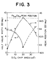
- Fig. 3 shows the half-value width and the peak position (2 ⁇ ) as the results of the X-ray diffraction respectively as functions of the SiO 2 chip area. It is clear from Fig. 3 that the half-value width decreases in proportion to the increase of the SiO 2 chip area, reaches the minimum at the chip area of 20 cm 2 , and then increases with the continued increase of the chip area. The peak position (2 ⁇ ) shifts toward the higher angle side in proportion to the increase of the SiO 2 chip area, reaches the maximum at the chip area of 20 cm 2 , and then shifts toward the lower angle side in proportion to the further continued increase of the chip area.
- the resistivity showed an inclination to increase in proportion to the increase of the SiO 2 chip area as shown in Fig 4 and the film of (c) having the SiO 2 chip area of 36 cm 2 showed resistivity of 2470 ⁇ cm.
- the films (a), (b), and (c) mentioned above invariably had an amorphous phase and that the resistivity of the amorphous phase manifested a predominant effect
- the films using SiO 2 chip areas of 0 to 20 cm 2 only acquired such magnitudes of resistivity as corresponded to their amorphous phases and that, in the films using SiO 2 chip areas exceeding 20 cm 2 and consequently entailing disappearance of their crystalline phases, the Si formerly concentrated within crystalline particles were uniformly distributed throughout the films and the magnitudes of resistivity within their amorphous phases suddenly increased.
- Table 2 and Fig. 5 show the film compositions obtained with the Ar pressure fixed at 1.6 Pa and the SiO 2 chip area varied. The data are based on the assumption that the total amount of the main components Fe, Co, Zr, and Si is 100 at%. It is noted from Table 2 that the ratios of combination of Fe, Co, and Zr substantially coincided with those in the targets at the time of charging.
- Fig. 5 is a diagram showing the relation between the amount (at.%) of Si in the produced films and the SiO 2 chip areas. This diagram shows that the proportion of Si in the composition increased substantially linearly in proportion to the increase of the SiO 2 chip area.
- Figs. 6A, 6B, 6C, and 6D show the magnetic hysteresis curves of the films as functions of SiO 2 chip areas.
- the solid lines represent the magnetic hysteresis curves in the direction of easy axis of magnetization and the broken lines those in the direction of hard axis of magnetization.
- the films having small SiO 2 chip areas (0 to 10 cm 2 ) manifested no anisotropy but were isotropic in the film plane (Figs. 6A, 6B).
- the film having the SiO 2 chip area of 20 cm 2 behaved like a vertical magnetic anisotropic film and was isotropic. It is inferred that the vertical magnetic anisotropy was derived from microcrystals having the (100) plane parallel to the surface of film.
- the film having the SiO 2 chip area of 36 cm 2 behaved like an in-plane magnetic anisotropic film. This behaviour may be explained by a supposition that the anisotropy of the sample shape which we used for magnetic properties measurement gained predominance because of the disappearance of microcrystals.
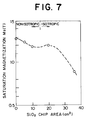
- Fig. 7 shows the saturation magnetization, M s , as a function of the SiO 2 chip area.
- the saturation magnetization, M s showed an inclination to decrease in proportion to the increase of the SiO 2 chip area. It is noted from this diagram that the soft magnetic characteristics necessary for a soft magnetic thin film to be used in a thin film magnetic element are retained even when the SiO 2 chip area is enlarged sufficiently to acquire resistivity levels exceeding 1000 ⁇ .cm.
- the soft magnetic thin film (having an SiO 2 chip area of 36 cm 2 ) according to the first embodiment acquires high resistivity of not less than 1000 ⁇ cm and retains soft magnetic characteristics necessary for a thin film magnetic element.
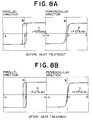
- Figs. 8A and 8B show changes caused in the magnetic hysteresis curve of a sample produced with an SiO 2 chip area of 36 cm 2 by a heat treatment performed at 573 K x one hour in a DC magnetic field of 120 kA/m. It is noted from Figs. 8A and 8B that the sample manifested conspicuous anisotropy after the heat treatment [Fig. 8B] as compared with the same sample before the heat treatment [Fig. 8A].
- a soft magnetic film 12 part of a thin film inductor 11 shown in a top view in Fig. 9A and in a cross section in Fig. 9B was manufactured.
- the thin film inductor 11 shown in Fig. 9 was constructed by superposing soft magnetic films 12, 12 on the opposite main surfaces of a double spiral type planar coil 13.
- the planar coil 13 was insulated from the soft magnetic films 12, 12 severally with an insulating layer 14.
- the thin film inductor 11 of this example acquired highly satisfactory properties as evinced by a substantially flat inductance up to 10 MHz and a quality factor, Q, of not less than 10 at 8 MHz.
- a thin film magnetic head 21 having a gap 24 shown in Fig. 10 was manufactured by the use of amorphous soft magnetic thin films 22 which were formed under the same conditions as used for the soft magnetic thin film of the example cited above. Specifically, the thin film magnetic head 21 was produced by coating one surface of a nonmagnetic glass substrate 23 with glass and having the amorphous soft magnetic thin films and the insulating films mentioned above alternately superposed to a prescribed thickness on the other surface of the nonmagnetic glass substrate 23.
- the soft magnetic thin films to be used for the thin film magnetic element of the embodiment 2 were obtained as follows. Ten SiO 2 chips measuring 10 mm x 10 mm x 2.3 mm were disposed evenly on an erosion pattern on disklike alloy targets having a composition of Fe 0.68 Co 0.17 Zr 0.15 and measuring 125 mm in diameter and 3 mm in thickness. The Fe 0.68 Co 0.17 Zr 0.15 alloy targets having 10 SiO 2 chips mounted thereon were set in place in an RF magnetron sputter device and sputtered on an Si substrate (0.6 mm in thickness) provided with a thermally oxidized SiO 2 coating.
- the power supplied for the sputtering was fixed at 3.3 W/cm 2 and the distance between the target and the substrate at 75 mm and the Ar gas pressure was varied in the range of 1.3 to 3.3 Pa.
- Fig. 11 shows the half-value width and the peak position (2 ⁇ ) as the results of the X-ray diffraction respectively as functions of the Ar gas pressure. It is clear from Fig. 11 that the half-value width and the peak position (2 ⁇ ) showed no extreme dependency on the Ar gas pressure. Films (d) and (e) formed by the sputtering under the conditions shown in Table 3 while using Ar gas pressures respectively of 1.6 Pa (d) and 3.3 Pa (e) were tested by the TEM observation.
- the film of (d) consisted of microcrystalline particles of a diameter of about 5 nm and an amorphous phase filling the gaps intervening between the microcrystalline particles and the film of (e) consisted of microcrystalline particles of a diameter of about 5 nm and two amorphous phases with clear contrast, one of which was disposed so as to fill the immediate neighborhoods of the microcrystalline particles and the other amorphous granular phase.
- the resistivity showed an inclination to increase in proportion to the increase of the Ar gas pressure as shown in Fig 12 and the film produced by using an Ar gas pressure of 3.3 Pa showed resistivity of 1440 ⁇ cm.
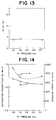
- Table 4 and Fig. 13 show the film compositions obtained as functions of the magnitudes of Ar pressure. The data are based on the assumption that the total amount of the main components Fe, Co, Zr, and Si is 100 at%. It is noted from Table 4 that the ratios of combination of Fe, Co, and Zr substantially coincided with those in the targets at the time of charging.
- Fig. 13 is a diagram showing the relation between the amount (at.%) of Si in the produced films and the Ar gas pressure. This diagram shows that the proportion of Si in the composition showed virtually no change relative to the Ar gas pressure. This fact indicates that the changes of the microstructure and the resistivity mentioned above were not brought about by changes in composition.
- Fig. 14 shows the saturation magnetization, M s , and the coercive force, H c , as functions of the Ar gas pressure. It is noted from the diagram that the saturation magnetization, M s , showed an inclination to decrease in proportion as the Ar gas pressure increased and the coercive force, H c , showed an inclination to decrease temporarily in proportion as the Ar gas pressure increased and an inclination to increase past the boundary of about 2 Pa with the continued increase of the Ar gas pressure. It is noted from this diagram that the soft magnetic character-istics necessary for a soft magnetic thin film to be used in a thin film magnetic element are retained even when the Ar gas pressure is increased to such an extent as to acquire a resistivity value exceeding 1000 ⁇ .cm.
- the soft magnetic thin film (produced by using an Ar gas pressure of 3.3 Pa) according to the present embodiment acquires high resistivity of not less than 1000 ⁇ cm and retains soft magnetic characteristics necessary for a thin film magnetic element.
- the thin film magnetic element in the embodiment 2 will be described below. Under the same conditions used for the mixed phase soft magnetic thin film as mentioned above, a soft magnetic film 12 part of a thin film inductor 11 shown in Figs. 9A and 9B was manufactured.
- the thin film inductor of this example acquired highly satisfactory properties as evinced by a substantially flat inductance up to 8 MHz and a quality factor, Q, of not less than 8 at 5 MHz.
- the thin film magnetic element of this invention can suppress the eddy current loss even at an operating frequency exceeding a high frequency zone of the level of MHz because it uses a soft magnetic thin film which simultaneously achieves high electric resistance and highly satisfactory saturation magnetic flux density.
- the thin film magnetic element of this invention When the thin film magnetic element of this invention is applied, for example, in a thin film magnetic head, it serves the purpose of enhancing the regeneration output of the magnetic head.
- a thin film inductor for example, it serves the purpose of improving the energy conversion efficiency.
Landscapes
- Engineering & Computer Science (AREA)
- Power Engineering (AREA)
- Microelectronics & Electronic Packaging (AREA)
- Thin Magnetic Films (AREA)
- Coils Or Transformers For Communication (AREA)
Applications Claiming Priority (3)
| Application Number | Priority Date | Filing Date | Title |
|---|---|---|---|
| JP7295595 | 1995-03-30 | ||
| JP72955/95 | 1995-03-30 | ||
| JP07295595A JP3759191B2 (ja) | 1995-03-30 | 1995-03-30 | 薄膜磁気素子 |
Publications (3)
| Publication Number | Publication Date |
|---|---|
| EP0735549A2 true EP0735549A2 (fr) | 1996-10-02 |
| EP0735549A3 EP0735549A3 (fr) | 1997-01-08 |
| EP0735549B1 EP0735549B1 (fr) | 2000-09-27 |
Family
ID=13504325
Family Applications (1)
| Application Number | Title | Priority Date | Filing Date |
|---|---|---|---|
| EP96302256A Expired - Lifetime EP0735549B1 (fr) | 1995-03-30 | 1996-03-29 | Film mince magnétiquement doux et élément magnétique à film mince l'utilisant |
Country Status (4)
| Country | Link |
|---|---|
| US (1) | US5750273A (fr) |
| EP (1) | EP0735549B1 (fr) |
| JP (1) | JP3759191B2 (fr) |
| DE (1) | DE69610453T2 (fr) |
Families Citing this family (13)
| Publication number | Priority date | Publication date | Assignee | Title |
|---|---|---|---|---|
| JPH09111419A (ja) * | 1995-10-16 | 1997-04-28 | Alps Electric Co Ltd | 磁気抵抗効果材料および磁気抵抗効果多層膜 |
| JPH1055916A (ja) * | 1996-08-08 | 1998-02-24 | Kiyoto Yamazawa | 薄型磁気素子およびトランス |
| JP3411194B2 (ja) * | 1997-07-29 | 2003-05-26 | アルプス電気株式会社 | 軟磁性膜及びこの軟磁性膜を用いたmr/インダクティブ複合型薄膜磁気ヘッド |
| JP3155234B2 (ja) * | 1997-09-17 | 2001-04-09 | アルプス電気株式会社 | 薄膜磁気ヘッドおよびその製造方法 |
| JPH11329837A (ja) * | 1998-03-10 | 1999-11-30 | Alps Electric Co Ltd | 磁性膜の成膜方法 |
| US6210544B1 (en) | 1999-03-08 | 2001-04-03 | Alps Electric Co., Ltd. | Magnetic film forming method |
| JP2001319314A (ja) * | 2000-02-29 | 2001-11-16 | Hitachi Ltd | 磁気記録媒体とその製法およびそれを用いた磁気記録装置 |
| US6815096B2 (en) | 2001-05-16 | 2004-11-09 | Tdk Corporation | Soft magnetic thin film and thin film magnetic head using the same |
| CA2577718A1 (fr) * | 2004-09-27 | 2006-04-06 | The Regents Of The University Of California | Acier amorphe economique |
| CN1331975C (zh) * | 2005-12-08 | 2007-08-15 | 南开大学 | 纳米晶铁锗颗粒薄膜磁敏材料 |
| TWI317954B (en) * | 2006-12-22 | 2009-12-01 | Ind Tech Res Inst | Soft magnetism thin film inductor and magnetic multi-element alloy film |
| US8986469B2 (en) | 2007-11-09 | 2015-03-24 | The Regents Of The University Of California | Amorphous alloy materials |
| CN101789488B (zh) * | 2010-03-12 | 2012-02-22 | 南开大学 | 用于霍尔元件的新型薄膜材料 |
Family Cites Families (5)
| Publication number | Priority date | Publication date | Assignee | Title |
|---|---|---|---|---|
| JPS6115941A (ja) * | 1984-06-30 | 1986-01-24 | Res Dev Corp Of Japan | 酸素を含む強磁性非晶質合金およびその製造法 |
| JPH0834154B2 (ja) * | 1986-11-06 | 1996-03-29 | ソニー株式会社 | 軟磁性薄膜 |
| JP2721562B2 (ja) * | 1989-03-08 | 1998-03-04 | アルプス電気株式会社 | 軟磁性合金膜 |
| JP2884599B2 (ja) * | 1989-06-30 | 1999-04-19 | ソニー株式会社 | 軟磁性非晶質膜 |
| JP2821627B2 (ja) * | 1989-09-20 | 1998-11-05 | ソニー株式会社 | 軟磁性非晶質合金薄膜 |
-
1995
- 1995-03-30 JP JP07295595A patent/JP3759191B2/ja not_active Expired - Fee Related
-
1996
- 1996-03-29 DE DE69610453T patent/DE69610453T2/de not_active Expired - Fee Related
- 1996-03-29 EP EP96302256A patent/EP0735549B1/fr not_active Expired - Lifetime
- 1996-03-29 US US08/623,529 patent/US5750273A/en not_active Expired - Fee Related
Also Published As
| Publication number | Publication date |
|---|---|
| JP3759191B2 (ja) | 2006-03-22 |
| US5750273A (en) | 1998-05-12 |
| DE69610453T2 (de) | 2001-05-10 |
| JPH08273930A (ja) | 1996-10-18 |
| EP0735549A3 (fr) | 1997-01-08 |
| DE69610453D1 (de) | 2000-11-02 |
| EP0735549B1 (fr) | 2000-09-27 |
Similar Documents
| Publication | Publication Date | Title |
|---|---|---|
| US6410170B1 (en) | High resistivity FeXN sputtered films for magnetic storage devices and method of fabrication | |
| EP0300511B1 (fr) | Tête magnétique | |
| EP0735549B1 (fr) | Film mince magnétiquement doux et élément magnétique à film mince l'utilisant | |
| JPH07268610A (ja) | 軟磁性合金薄膜 | |
| JPH07220922A (ja) | 平面型磁気素子および非晶質磁性薄膜 | |
| US6238492B1 (en) | Soft magnetic thin film, method for preparing same and magnetic head | |
| US5302469A (en) | Soft magnetic thin film | |
| JPH02229406A (ja) | 軟磁性合金膜 | |
| JPH0744108B2 (ja) | 軟磁性薄膜 | |
| EP0342922B1 (fr) | Alliage magnétique mou à base de fer et noyau en poudre fait à partir de celui-ci | |
| US5133814A (en) | Soft magnetic thin film | |
| JP2950917B2 (ja) | 軟磁性薄膜 | |
| US5786103A (en) | Soft magnetic film and magnetic head employing same | |
| US4743313A (en) | Amorphous alloy for use in magnetic heads | |
| JP2866911B2 (ja) | 磁気ヘッド | |
| US6303240B1 (en) | Soft magnetic thin film | |
| JP2925257B2 (ja) | 強磁性膜、その製造方法及び磁気ヘッド | |
| JP2784105B2 (ja) | 軟磁性薄膜 | |
| JPH0636928A (ja) | 軟磁性材料 | |
| JP2508462B2 (ja) | 軟磁性薄膜 | |
| JP3233538B2 (ja) | 軟磁性合金、軟磁性薄膜および多層膜 | |
| JP2522284B2 (ja) | 軟磁性薄膜 | |
| JP2808547B2 (ja) | 複合磁気ヘッド | |
| JPH0546922A (ja) | 軟磁性合金及びそれを用いた磁気ヘツド | |
| JPH07118054B2 (ja) | Mig型磁気ヘッドの製造方法 |
Legal Events
| Date | Code | Title | Description |
|---|---|---|---|
| PUAI | Public reference made under article 153(3) epc to a published international application that has entered the european phase |
Free format text: ORIGINAL CODE: 0009012 |
|
| 17P | Request for examination filed |
Effective date: 19960424 |
|
| AK | Designated contracting states |
Kind code of ref document: A2 Designated state(s): DE FR |
|
| PUAL | Search report despatched |
Free format text: ORIGINAL CODE: 0009013 |
|
| AK | Designated contracting states |
Kind code of ref document: A3 Designated state(s): DE FR |
|
| GRAG | Despatch of communication of intention to grant |
Free format text: ORIGINAL CODE: EPIDOS AGRA |
|
| GRAG | Despatch of communication of intention to grant |
Free format text: ORIGINAL CODE: EPIDOS AGRA |
|
| GRAH | Despatch of communication of intention to grant a patent |
Free format text: ORIGINAL CODE: EPIDOS IGRA |
|
| 17Q | First examination report despatched |
Effective date: 20000222 |
|
| GRAH | Despatch of communication of intention to grant a patent |
Free format text: ORIGINAL CODE: EPIDOS IGRA |
|
| GRAA | (expected) grant |
Free format text: ORIGINAL CODE: 0009210 |
|
| AK | Designated contracting states |
Kind code of ref document: B1 Designated state(s): DE FR |
|
| RIN1 | Information on inventor provided before grant (corrected) |
Inventor name: FUKE, HIROMI, C/O K.K. TOSHIBA I.P.D. Inventor name: MIZOGUCHI, TETSUHIKO, C/O K.K. TOSHIBA I.P.D. Inventor name: TOMITA, HIROSHI, C/O K.K. TOSHIBA I.P.D. Inventor name: INOUE, TETSUO, C/O K.K TOSHIBA I.P.D. |
|
| ET | Fr: translation filed | ||
| REF | Corresponds to: |
Ref document number: 69610453 Country of ref document: DE Date of ref document: 20001102 |
|
| PLBE | No opposition filed within time limit |
Free format text: ORIGINAL CODE: 0009261 |
|
| STAA | Information on the status of an ep patent application or granted ep patent |
Free format text: STATUS: NO OPPOSITION FILED WITHIN TIME LIMIT |
|
| 26N | No opposition filed | ||
| PGFP | Annual fee paid to national office [announced via postgrant information from national office to epo] |
Ref country code: DE Payment date: 20090327 Year of fee payment: 14 |
|
| PGFP | Annual fee paid to national office [announced via postgrant information from national office to epo] |
Ref country code: FR Payment date: 20090316 Year of fee payment: 14 |
|
| REG | Reference to a national code |
Ref country code: FR Ref legal event code: ST Effective date: 20101130 |
|
| PG25 | Lapsed in a contracting state [announced via postgrant information from national office to epo] |
Ref country code: FR Free format text: LAPSE BECAUSE OF NON-PAYMENT OF DUE FEES Effective date: 20100331 |
|
| PG25 | Lapsed in a contracting state [announced via postgrant information from national office to epo] |
Ref country code: DE Free format text: LAPSE BECAUSE OF NON-PAYMENT OF DUE FEES Effective date: 20101001 |