EP0735560B1 - Breitbandige Wanderfeldröhre - Google Patents
Breitbandige Wanderfeldröhre Download PDFInfo
- Publication number
- EP0735560B1 EP0735560B1 EP96105138A EP96105138A EP0735560B1 EP 0735560 B1 EP0735560 B1 EP 0735560B1 EP 96105138 A EP96105138 A EP 96105138A EP 96105138 A EP96105138 A EP 96105138A EP 0735560 B1 EP0735560 B1 EP 0735560B1
- Authority
- EP
- European Patent Office
- Prior art keywords
- waveguide
- helix
- wave
- broad
- spacers
- Prior art date
- Legal status (The legal status is an assumption and is not a legal conclusion. Google has not performed a legal analysis and makes no representation as to the accuracy of the status listed.)
- Expired - Lifetime
Links
- 125000006850 spacer group Chemical group 0.000 claims description 28
- 230000000994 depressogenic effect Effects 0.000 claims 2
- 230000003993 interaction Effects 0.000 description 19
- 238000010894 electron beam technology Methods 0.000 description 15
- 230000000694 effects Effects 0.000 description 10
- 239000000696 magnetic material Substances 0.000 description 5
- 230000007423 decrease Effects 0.000 description 3
- 230000003247 decreasing effect Effects 0.000 description 3
- XEEYBQQBJWHFJM-UHFFFAOYSA-N Iron Chemical compound [Fe] XEEYBQQBJWHFJM-UHFFFAOYSA-N 0.000 description 2
- ZOKXTWBITQBERF-UHFFFAOYSA-N Molybdenum Chemical compound [Mo] ZOKXTWBITQBERF-UHFFFAOYSA-N 0.000 description 2
- 230000005672 electromagnetic field Effects 0.000 description 2
- 229910052751 metal Inorganic materials 0.000 description 2
- 239000002184 metal Substances 0.000 description 2
- 238000000034 method Methods 0.000 description 2
- 229910052750 molybdenum Inorganic materials 0.000 description 2
- 239000011733 molybdenum Substances 0.000 description 2
- WFKWXMTUELFFGS-UHFFFAOYSA-N tungsten Chemical compound [W] WFKWXMTUELFFGS-UHFFFAOYSA-N 0.000 description 2
- 229910052721 tungsten Inorganic materials 0.000 description 2
- 239000010937 tungsten Substances 0.000 description 2
- 230000003321 amplification Effects 0.000 description 1
- 230000008901 benefit Effects 0.000 description 1
- 238000005219 brazing Methods 0.000 description 1
- 230000008859 change Effects 0.000 description 1
- 230000001419 dependent effect Effects 0.000 description 1
- 238000012938 design process Methods 0.000 description 1
- 238000011161 development Methods 0.000 description 1
- 230000018109 developmental process Effects 0.000 description 1
- 230000004927 fusion Effects 0.000 description 1
- 238000010438 heat treatment Methods 0.000 description 1
- 230000006872 improvement Effects 0.000 description 1
- 229910052742 iron Inorganic materials 0.000 description 1
- 238000004519 manufacturing process Methods 0.000 description 1
- 238000005259 measurement Methods 0.000 description 1
- 238000012986 modification Methods 0.000 description 1
- 230000004048 modification Effects 0.000 description 1
- 238000003199 nucleic acid amplification method Methods 0.000 description 1
- 239000002245 particle Substances 0.000 description 1
- 230000004044 response Effects 0.000 description 1
Images


Classifications
-
- H—ELECTRICITY
- H01—ELECTRIC ELEMENTS
- H01J—ELECTRIC DISCHARGE TUBES OR DISCHARGE LAMPS
- H01J23/00—Details of transit-time tubes of the types covered by group H01J25/00
- H01J23/16—Circuit elements, having distributed capacitance and inductance, structurally associated with the tube and interacting with the discharge
- H01J23/24—Slow-wave structures, e.g. delay systems
- H01J23/26—Helical slow-wave structures; Adjustment therefor
Definitions
- the present invention relates to a travelling-wave tube and more particularly, to a broad-band travelling-wave tube that is effectively used for power amplification at microwave frequencies.
- the microwave power is in wide spread use in such a variety of application fields as communications, Electro Counter Measure (ECM), radar, industrial heating, particle accelerator, radio astronomy, and nuclear fusion.
- ECM Electro Counter Measure
- radar To meet the demand of society for realizing a high-level of information society for the coming century, the field of communications among the above various fields has been increasingly becoming important in application of microwave power.
- a "traveling-wave tube” that uses an electron beam to amplify microwave power is available.
- the traveling-wave tube has a slow-wave structure that provides an interaction between a microwave input signal and an electron beam.
- a typical slow-wave structure is a helix, which is coaxially arranged in a cylindrical waveguide.
- the helix is held by dielectric supports not to be contacted with the waveguide.
- the helix provides such features as simple structure, easy fabrication, and broad-band functioning capability and therefore, it has been widely applied.
- FIG. 1 An example of the conventional traveling-wave tubes equipped with the helix-type slow-wave structure is shown in Fig. 1.
- this travelling-wave tube is partitioned into three sections, i.e., an electron beam (E-beam) source section 10, an interaction section 20, and a collector section 30.
- E-beam electron beam
- the interaction section 20 an interaction between the electron beam EB emitted from the source section 10 and a radio-frequency (RF) electro-magnetic field caused by an applied microwave input signal takes place.
- RF radio-frequency
- the traveling-wave tube has a cylindrical vacuum envelope 1, an electron gun 11 fixed to one end of the envelope 1, and a collector 31 fixed to the other end thereof.
- a focusing electrode 12 is fixed to focus or narrow the electron beam EB emitted from the gun 11.
- the electron gun 11 and the focusing electrode 12 constitute the E-beam source section 10.
- a conductive helix 21 forming a slow-wave structure is provided in a cylindrical waveguide 26 to be coaxial therewith.
- the helix 21 is made of a metal such as molybdenum (Mo) or tungsten (W).
- Mo molybdenum
- W tungsten
- the helix 21 is held by dielectric supports 22 placed between the helix 21 and the inner wall of the waveguide 26.
- Both ends of the helix 21 protrude outside from the vacuum envelope 1.
- a microwave input signal is supplied to the helix 21 through its one end.
- the input signal is amplified in the interaction section 20 due to the interaction between the traveling electron beam EB and the RF field caused by the input signal and then, it is taken out through the other end.
- the waveguide 26 is made of a plurality of pole pieces 23 and a plurality of spacers 24 which are alternately arranged along the axis of the cylindrical vacuum envelope 1 and which are coupled together.
- the pole pieces 23 are made of a magnetic material.
- the spacers 24 are made of a non-magnetic material.
- the pole pieces 23 are of a circular ring shape and have cylindrical cavities therein.
- the spacers 24 are also of a circular ring shape and have cylindrical cavities therein. The pole pieces 23 and the spacers 24 are connected together to couple their cavities with each other, thereby producing the cylindrical waveguide 26.
- the magnet pieces 25 are arranged at regular intervals along the axis of the waveguide 26.
- the magnet pieces 25 and the pole pieces 23 produce a focusing magnetic field that focuses the electron beam EB travelling through the waveguide 26.
- the interaction section 20 contains the helix 21, supports 22, pole pieces 23, spacers 24 and magnet pieces 25.
- the interaction section 20 is further partitioned into an input subsection 20a and an output subsection 20b. Electric power is given to the microwave input signal in the input subsection 20a, and the electric power thus given is taken out in the output subsection 20b.
- the electron beam EB having passed through the waveguide 26 in the interaction section 20 is collected by a collector 31 disposed in the collector section 30.
- the slow-wave structure With the conventional traveling-wave tube shown in Fig. 1, to make the slow-wave structure suitable for broad-band applications such as communications, the slow-wave structure must have a response as flat as possible over a wide range of microeave frequencies. Especially, in recent years, the operation band of the traveling-wave tube has been required to be ultra broad for use in such applications as communications, ECM, and radar. However, the interaction between the electron beam EB and the RF field tends to greatly vary depending upon the frequency and consequently, it is difficult for the slow-wave structure of the above conventional tube to realize a broad-band functioning capability.
- vanes 27 are fixed onto the inner wall 26a of the waveguide 26, thereby forming offsets on the wall 26a.
- the phase velocity of a traveling wave through the slow-wave structure can be made substantially uniform for frequency.
- this improved structure is effective for providing a broad-band functioning capability.
- the Japanese Non-Examined Utility-Model Publication No. 4-85637 also disclosed the structure as shown in Fig. 3, where projections 28 are formed on the inner wall 16a of the waveguide 26 instead of the vanes 27.
- the projections 28 are made by deforming the wall 26a toward inside. This variation can provide the same effect as that of Fig. 2.
- phase velocity of a wave traveling through the slow-wave structure tends to slightly decrease with the decreasing value of the ratio (a v /a). This phase-velocity decreasing effect is more conspicuous at lower frequencies.
- the value of the ratio (a v /a) is greater than a certain value, the phase velocity scarcely varies even with the frequency change.
- the value of the ratio (a v /a) is reduced to the certain value or less, the phase velocity tends to decrease with lowering the frequency.
- vanes 27 tends to be more conspicuous as the value of ⁇ t increases. Accordingly, in the actual design process, a compromise between the values of (a v /a) and ⁇ t is found to thereby provide a phase velocity as uniform as possible over a wide frequency range, thus making the microwave tube suitable for use in broad-band applications.
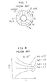
- Fig. 6 shows the relationship between the frequency f and the phase velocity v p disclosed in the above article, where the frequency f is normalized by the frequency f 0 and the phase velocity v p is normalized by the light speed c.
- the curve A shows the relationship obtained by actual measurement and the curve B shows the relationship obtained by calculation.
- the average radius of the helix 21 is approximately 1.5 mm
- the bore diameter of the vanes 27 is approximately 2 mm
- the angular periodicity ⁇ t is 40° to 70°
- the angular thickness of the dielectric supports 22 is approximately 0.5 mm.
- the angular thickness of the vanes 27 becomes approximately 1.5 mm.
- a broad-band travelling-wave tube according to the preamble of claim 1 is disclosed in Patents Abstracts of Japan JP-A-63218123.
- This tube comprises non-magnetic cylinders and pole pieces arranged alternately along the longitudinal axis of the tube, wherein the inner wall of the non-magnetic cylinders have smaller diameters than the pole pieces and wherein grooves extending in axial direction are provided in the non-magnetic cylinders in which axial extending helix holding rods are inserted.
- Another object of the present invention is to provide a broad-band travelling-wave tube that can be fabricated even for use in the milimeter wave-band.
- a broad-band traveling-wave tube contains a waveguide made of a plurality of pole pieces and a plurality of spacers which are alternately arranged along the axis of the waveguide.
- the inner wall of the waveguide has a plurality of offsets arranged at intervals along the axis of the waveguide.
- the inner wall of the waveguide which is made of the plurality of pole pieces and the plurality of spacers, has a plurality of offsets arranged at intervals along the axis of the waveguide. Therefore, an equivalent effect to that of the conventional vanes is obtained. This means that a broad-band traveling-wave tube can be obtained without using the conventional vanes.
- the broad-band traveling-wave tube according to the invention uses no vanes and therefore, a broad-band traveling-wave tube for use in the millimeter wave band can be fabricated.
- Fig. 1 is a schematic, axial cross-sectional view of a conventional traveling-wave tube.
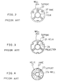
- Fig. 2 is a schematic, radial cross-sectional view of a first example of conventional slow-wave structures.
- Fig. 3 is a schematic, radial cross-sectional view of a second example of conventional slow-wave structures.
- Fig. 4 is a schematic radial cross-sectional view of a third example of conventional slow-wave structures.
- Fig. 5 is a schematic, radial cross-sectional view of a fourth example of conventional slow-wave structures.
- Fig. 6 is a graph showing the relationship of the phase velocity with the frequency for a conventional broad-band traveling-wave tube.
- Fig. 7 is a schematic, radial cross-sectional view of the first example of conventional slow-wave structures.
- Fig. 8 is a graph showing the relationship between the phase velocity and the frequency for the conventional broad-band traveling-wave tube.
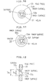
- Fig. 9 is a schematic, axial cross-sectional view of a waveguide for a slow-wave structure according to a first embodiment of the invention.
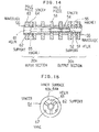
- Fig. 10 is a schematic, radial cross-sectional view of the pole piece, which is used for the waveguide according to the first embodiment.
- Fig. 11 is a schematic, radial cross-sectional view of the spacer, which is used for the waveguide according to the first embodiment.
- Fig. 12 is a schematic, axial cross-sectional view of the pole piece, which is used for the waveguide according to the first embodiment.
- Fig. 13 is a schematic, axial cross-sectional view of the spacer, which is used for the waveguide according to the first embodiment.
- Fig. 14 is a schematic, axial cross-sectional view of a waveguide for a slow-wave structure according to a second embodiment of the invention.
- Fig. 15 is a schematic, radial cross-sectional view of the spacer placed in the input subsection, which is used for the waveguide according to the second embodiment.
- a broad-band traveling-wave tube according to a first embodiment of the present invention has the same basic structure as that of the conventional one shown in Fig. 1. Therefore, the description relating to the same structure is omitted here for the sake of simplicity and only the different structures from the conventional one are explained below.
- the traveling-wave tube according to the first embodiment is equipped with a waveguide 56 as shown in Fig. 9 in the interaction section 20.
- the waveguide 56 is composed of a plurality of pole pieces 53 and a plurality of spacers 54, which are alternately arranged along the axis of the cylindrical vacuum envelope 1 and which are coupled together by brazing.
- the pole pieces 53 are made of a magnetic material.
- the spacers 54 are made of a non-magnetic material.
- Each of the pole pieces 53 has a circular ring shape and an approximately cylindrical cavity therein.
- Each of the spacers 54 also has a circular ring shape and an approximately cylindrical cavity therein. The cavities of the pole pieces 53 and those of the spacers 54 are connected together to thereby produce the cylindrical waveguide 56.
- a plurality of permanent magnet pieces 55 which have a circular ring shape, are placed outside the respective spacers 54.
- the magnet pieces 55 are arranged at regular intervals along the axis of the waveguide 56.
- the magnet pieces 55 and the pole pieces 53 produce a focusing magnetic field that focuses the electron beam EB travelling through the waveguide 56.
- a conductive helix 51 forming a slow-wave structure is provided in the waveguide 56 to be coaxial therewith.
- the helix 51 is made of a metal such as molybdenum (Mo) or tungsten (W).
- Mo molybdenum
- W tungsten
- the helix 51 is held by three dielectric supports 52 placed between the helix 51 and the inner wall of the waveguide 56.
- the supports 52 which have a shape of a straight bar, extend along the axis of the helix 51 from one end of the helix 51 to the other end thereof.
- Both ends of the helix 51 protrude outside from the vacuum envelope 1.
- a microwave input signal is supplied to the helix 51 through its one end.
- the input signal is amplified in the interaction section 20 due to the interaction between the traveling electron beam EB and the RF field caused by the input signal and then, it is taken out through the other end.
- each of the pole pieces 53 has two circumferential grooves or depressions 53c at each end.
- the inner surface 53a of the piece 53 has a relatively smaller diameter D p1 .
- the inner surface 53b of the piece 53, which is the bottom of the groove 53c, has a relatively larger diameter D p2 .
- each of the spacers 54 has two circumferential grooves or depressions 54c formed at regular intervals along the axis of the spacer 54.
- the traveling-wave tube according to the first embodiment since the grooves 53c and 54c are periodically arranged along the axis of the waveguide 56 to thereby produce a plurality of offsets on the inner wall of the waveguide 56, an equivalent effect to that of the conventional vanes is obtained. As a result, a broad-band traveling-wave tube can be obtained without using the conventional vanes.
- the broad-band traveling-wave tube according to the first embodiment uses no vanes and therefore, a broad-band traveling-wave tube for use in the millimeter wave band can be fabricated.
- the equivalent effect is due to hollow spaces generated by the offsets.
- the waveguide is divided into three sets of four different regions R 1 , R 2 , R 3 and R 4 , which are arranged at angular intervals of 120°, as shown in Fig. 7.
- the region R 1 the vane exists and therefore, the inner diameter of the bore is relatively small.
- the region R 2 no vane and no support exist and therefore, the inner diameter of the bore is relatively large.
- the region R 3 the support exists.
- the region R 4 no vane and no support exist and therefore, the inner diameter of the bore is relatively large, which is identical with the region R 2 .
- phase velocity of a wave traveling through the interaction section 20 for frequency provides the relationship of Fig. 8. From Fig. 8, it is seen that, depending upon the selected value of (a v /a), the phase velocity can be made substantially uniform with the changing frequency, and thus the broad-band functioning capability can be provided. This tendency also depends upon the selected value of the angular periodicity ⁇ t of the vane.
- the slow-wave circuit including the vanes is treated as a model in which the helix is developed along a linear line and the helix supports are arranged in parallel to the linear line with respect to the electro-magnetic field that travels along the helix, while rotating.
- the present invention utilizes this principle and consequently, the same effects as those by the conventional tube can be obtained.
- the smaller bore diameter must be specified to be approximately 1.5 to 2 times the average radius of the helix 51 so that the phase velocity is substantially uniform with respect to the frequency, while the larger bore diameter must be 2 to 3 times as large as the average radius of the helix 51.
- the reasons why such smaller and larger bore diameters are specified are that, if the larger bore diameter exceeds the above upper limit, the required bore diameter of the electron-beam focusing magnet 55 increases, resulting in the required magnetic field being not achieved, and thus focusing the electron beam being difficult, and that, if the smaller bore diameter is under the lower limit, the impedance of the interaction section 20 decreases, resulting in the lowered efficiency of the microwave tube.
- the pole pieces 53 are preferably made of iron, and are approximately half as thick as the spacers 54, which is made of a non-magnetic material. In addition, the thickness of the pole pieces 53 and that of the spacers 54 is preferably minimized so long as the proper magnetic field for focusing can be obtained.
- FIGs. 14 and 15 A broad-band traveling-wave tube according to a second embodiment of the present invention is shown in Figs. 14 and 15.
- the difference of the second embodiment from the first embodiment is that only the waveguide 56 for the output subsection 20b of the interaction section 20 contains the offsets while a waveguide 66 for the input subsection 20a does not contain offsets.
- the waveguide 66 has conventional vanes (not shown).
- the other structure is the same as that of the first embodiment.
- the second embodiment is equivalent to a tube which is obtained by applying the present invention to a vane-loaded traveling-wave tube.
Landscapes
- Microwave Tubes (AREA)
Claims (3)
- Breitband-Wanderfeldröhre mit:dadurch gekennzeichnet, daßeinem Wellenleiter (56, 66) aus einer Anzahl von Polstükken (53, 63) und einer Anzahl von Abstandshaltern (54, 64), die abwechselnd entlang der Achse des Wellenleiters angeordnet sind,einer Wendel (51, 61), die in dem Wellenleiter entlang der Achse des Wellenleiters angeordnet ist, undeinem Wendelträger (52, 62) zum Tragen der Wendel, wobei der Wendelträger zwischen der Innenwand des Wellenleiters und der Wendel angeordnet ist,die Innenwand des Wellenleiters eine Anzahl von Umfangsabsätzen (53c, 54c) aufweist, die in Intervallen entlang der Achse des Wellenleiters angeordnet sind,wobei die Umfangsabsätze durch nach außen eingerückte Bereiche oder nach innen vorstehende Bereiche gebildet sind, die auf den Innenflächen der Polstücke (53) und solchen der Abstandshalter (54) gebildet sind.
- Röhre nach Anspruch 1,
wobei der Wellenleiter in einen ersten Teil (20a) für einen Eingabe-Unterabschnitt und einen zweiten Teil (20b) für einen Ausgabeunterabschnitt unterteilt ist und wobei nur der zweite Teil (20b) die Absätze aufweist. - Röhre nach Anspruch 1,
wobei die Innenflächen der Polstücke (53, 63) im wesentlichen gleichen Durchmesser wie die Innenflächen der Abstandshalter (54) aufweisen und wobei die nach außen eingerückten Bereiche oder die nach innen vorstehenden Bereiche der Polstücke im wesentlichen den gleichen Durchmesser wie die Abstandshalter aufweisen.
Applications Claiming Priority (3)
| Application Number | Priority Date | Filing Date | Title |
|---|---|---|---|
| JP7512395 | 1995-03-31 | ||
| JP75123/95 | 1995-03-31 | ||
| JP7075123A JP2739833B2 (ja) | 1995-03-31 | 1995-03-31 | 広帯域進行波管 |
Publications (2)
| Publication Number | Publication Date |
|---|---|
| EP0735560A1 EP0735560A1 (de) | 1996-10-02 |
| EP0735560B1 true EP0735560B1 (de) | 2000-08-16 |
Family
ID=13567119
Family Applications (1)
| Application Number | Title | Priority Date | Filing Date |
|---|---|---|---|
| EP96105138A Expired - Lifetime EP0735560B1 (de) | 1995-03-31 | 1996-03-29 | Breitbandige Wanderfeldröhre |
Country Status (4)
| Country | Link |
|---|---|
| US (1) | US5754006A (de) |
| EP (1) | EP0735560B1 (de) |
| JP (1) | JP2739833B2 (de) |
| DE (1) | DE69609752T2 (de) |
Cited By (1)
| Publication number | Priority date | Publication date | Assignee | Title |
|---|---|---|---|---|
| CN112349566A (zh) * | 2020-09-23 | 2021-02-09 | 电子科技大学 | 一种改善毫米波螺旋线行波管驻波系数的装置 |
Families Citing this family (5)
| Publication number | Priority date | Publication date | Assignee | Title |
|---|---|---|---|---|
| US6747412B2 (en) * | 2001-05-11 | 2004-06-08 | Bernard K. Vancil | Traveling wave tube and method of manufacture |
| US6917162B2 (en) * | 2002-02-13 | 2005-07-12 | Genvac Aerospace Corporation | Traveling wave tube |
| US7315126B2 (en) * | 2004-11-04 | 2008-01-01 | L-3 Communications Corporation | Folded waveguide traveling wave tube having polepiece-cavity coupled-cavity circuit |
| KR101697039B1 (ko) * | 2007-02-21 | 2017-01-16 | 테라피직스 코포레이션 | 고주파 나선 증폭기와 발진기 |
| CN102917529B (zh) * | 2012-10-24 | 2016-01-13 | 中国科学院近代物理研究所 | 螺旋型多间隙高频谐振装置及聚束和加速方法 |
Family Cites Families (12)
| Publication number | Priority date | Publication date | Assignee | Title |
|---|---|---|---|---|
| US3293478A (en) * | 1963-03-28 | 1966-12-20 | Gen Electric | Traveling wave tube with longitudinal recess |
| US3398314A (en) * | 1964-11-18 | 1968-08-20 | Westinghouse Electric Corp | Traveling wave tube having means for removing slow electrons from electron beam |
| US3551729A (en) * | 1969-06-25 | 1970-12-29 | Bell Telephone Labor Inc | Traveling wave tube helix support structure |
| US3654509A (en) * | 1970-12-14 | 1972-04-04 | Varian Associates | Dielectrically supported helix derived slow wave circuit |
| GB1451956A (en) * | 1973-02-16 | 1976-10-06 | English Electric Valve Co Ltd | Travelling wave tubes |
| US3809949A (en) * | 1973-02-20 | 1974-05-07 | Varian Associates | Apparatus for increasing rf conversion efficiency of a traveling wave tube |
| JPS63218123A (ja) * | 1987-03-05 | 1988-09-12 | Toshiba Corp | 進行波管 |
| JPH03116634A (ja) * | 1989-09-28 | 1991-05-17 | Nec Corp | マイクロ波管 |
| JPH0485637A (ja) * | 1990-07-30 | 1992-03-18 | Fujitsu Ltd | 動的領域管理方式 |
| JPH0498737A (ja) * | 1990-08-15 | 1992-03-31 | Nec Corp | ヘリックス形遅波回路 |
| JPH0498736A (ja) * | 1990-08-15 | 1992-03-31 | Nec Corp | ヘリックス形進行波管の製造方法 |
| JPH05205645A (ja) * | 1992-01-27 | 1993-08-13 | Toshiba Corp | 進行波管の遅波回路構造体の製造方法 |
-
1995
- 1995-03-31 JP JP7075123A patent/JP2739833B2/ja not_active Expired - Fee Related
-
1996
- 1996-03-29 EP EP96105138A patent/EP0735560B1/de not_active Expired - Lifetime
- 1996-03-29 DE DE69609752T patent/DE69609752T2/de not_active Expired - Fee Related
- 1996-04-01 US US08/617,729 patent/US5754006A/en not_active Expired - Lifetime
Cited By (2)
| Publication number | Priority date | Publication date | Assignee | Title |
|---|---|---|---|---|
| CN112349566A (zh) * | 2020-09-23 | 2021-02-09 | 电子科技大学 | 一种改善毫米波螺旋线行波管驻波系数的装置 |
| CN112349566B (zh) * | 2020-09-23 | 2022-02-01 | 电子科技大学 | 一种改善毫米波螺旋线行波管驻波系数的装置 |
Also Published As
| Publication number | Publication date |
|---|---|
| DE69609752T2 (de) | 2001-04-12 |
| EP0735560A1 (de) | 1996-10-02 |
| DE69609752D1 (de) | 2000-09-21 |
| US5754006A (en) | 1998-05-19 |
| JP2739833B2 (ja) | 1998-04-15 |
| JPH08273549A (ja) | 1996-10-18 |
Similar Documents
| Publication | Publication Date | Title |
|---|---|---|
| US4851788A (en) | Mode suppressors for whispering gallery gyrotron | |
| US4229676A (en) | Helical slow-wave structure assemblies and fabrication methods | |
| US2957103A (en) | High power microwave tube | |
| EP0735560B1 (de) | Breitbandige Wanderfeldröhre | |
| EP0660363B1 (de) | Linearstrahl-Hohlräumeschaltungen mit nicht resonanten RF-Dämpfungsplatten | |
| US3069594A (en) | Electron discharge devices | |
| US4912366A (en) | Coaxial traveling wave tube amplifier | |
| US3413512A (en) | Undulating, slow wave structure for an electron discharge device | |
| US3886397A (en) | Hybrid slow wave circuit | |
| US4621219A (en) | Electron beam scrambler | |
| US4481444A (en) | Traveling wave tubes having backward wave suppressor devices | |
| US5315210A (en) | Klystron resonant cavity operating in TM01X mode, where X is greater than zero | |
| US4866343A (en) | Re-entrant double-staggered ladder circuit | |
| US4513223A (en) | Electron tube with transverse cyclotron interaction | |
| CN115083866B (zh) | 一种正弦型曲折波导慢波组件及行波管 | |
| JPH0320933A (ja) | らせん遅延線の構成法およびこの構成モードによる進行波管 | |
| US4531103A (en) | Multidiameter cavity for reduced mode competition in gyrotron oscillator | |
| US4742271A (en) | Radial-gain/axial-gain crossed-field amplifier (radaxtron) | |
| JP2000215820A (ja) | ヘリックス型遅波回路 | |
| CA2013366A1 (en) | Klystron with reduced length | |
| US3054018A (en) | Traveling wave amplifier tube | |
| JPH08129960A (ja) | 多空胴クライストロン | |
| Pchelnikov | Old Know‐How in Helix TWT Development in the USSR | |
| JP2551351B2 (ja) | クライストロン | |
| US3278792A (en) | Apparatus for suppression of backward wave oscillation in traveling wave tubes having bifilar helical wave structure |
Legal Events
| Date | Code | Title | Description |
|---|---|---|---|
| PUAI | Public reference made under article 153(3) epc to a published international application that has entered the european phase |
Free format text: ORIGINAL CODE: 0009012 |
|
| AK | Designated contracting states |
Kind code of ref document: A1 Designated state(s): DE FR GB |
|
| 17P | Request for examination filed |
Effective date: 19960820 |
|
| 17Q | First examination report despatched |
Effective date: 19971104 |
|
| GRAG | Despatch of communication of intention to grant |
Free format text: ORIGINAL CODE: EPIDOS AGRA |
|
| GRAG | Despatch of communication of intention to grant |
Free format text: ORIGINAL CODE: EPIDOS AGRA |
|
| GRAH | Despatch of communication of intention to grant a patent |
Free format text: ORIGINAL CODE: EPIDOS IGRA |
|
| GRAH | Despatch of communication of intention to grant a patent |
Free format text: ORIGINAL CODE: EPIDOS IGRA |
|
| GRAA | (expected) grant |
Free format text: ORIGINAL CODE: 0009210 |
|
| AK | Designated contracting states |
Kind code of ref document: B1 Designated state(s): DE FR GB |
|
| REF | Corresponds to: |
Ref document number: 69609752 Country of ref document: DE Date of ref document: 20000921 |
|
| ET | Fr: translation filed | ||
| PLBE | No opposition filed within time limit |
Free format text: ORIGINAL CODE: 0009261 |
|
| STAA | Information on the status of an ep patent application or granted ep patent |
Free format text: STATUS: NO OPPOSITION FILED WITHIN TIME LIMIT |
|
| 26N | No opposition filed | ||
| REG | Reference to a national code |
Ref country code: GB Ref legal event code: IF02 |
|
| REG | Reference to a national code |
Ref country code: GB Ref legal event code: 732E |
|
| REG | Reference to a national code |
Ref country code: FR Ref legal event code: TP |
|
| PGFP | Annual fee paid to national office [announced via postgrant information from national office to epo] |
Ref country code: DE Payment date: 20070322 Year of fee payment: 12 |
|
| PGFP | Annual fee paid to national office [announced via postgrant information from national office to epo] |
Ref country code: GB Payment date: 20070328 Year of fee payment: 12 |
|
| GBPC | Gb: european patent ceased through non-payment of renewal fee |
Effective date: 20080329 |
|
| PG25 | Lapsed in a contracting state [announced via postgrant information from national office to epo] |
Ref country code: DE Free format text: LAPSE BECAUSE OF NON-PAYMENT OF DUE FEES Effective date: 20081001 |
|
| PG25 | Lapsed in a contracting state [announced via postgrant information from national office to epo] |
Ref country code: GB Free format text: LAPSE BECAUSE OF NON-PAYMENT OF DUE FEES Effective date: 20080329 |
|
| PGFP | Annual fee paid to national office [announced via postgrant information from national office to epo] |
Ref country code: FR Payment date: 20100324 Year of fee payment: 15 |
|
| REG | Reference to a national code |
Ref country code: FR Ref legal event code: TP |
|
| REG | Reference to a national code |
Ref country code: FR Ref legal event code: ST Effective date: 20111130 |
|
| PG25 | Lapsed in a contracting state [announced via postgrant information from national office to epo] |
Ref country code: FR Free format text: LAPSE BECAUSE OF NON-PAYMENT OF DUE FEES Effective date: 20110331 |