EP0735598A2 - Dispositif émetteur de lumière à composé semi-conducteur et méthode de fabrication - Google Patents
Dispositif émetteur de lumière à composé semi-conducteur et méthode de fabrication Download PDFInfo
- Publication number
- EP0735598A2 EP0735598A2 EP96103584A EP96103584A EP0735598A2 EP 0735598 A2 EP0735598 A2 EP 0735598A2 EP 96103584 A EP96103584 A EP 96103584A EP 96103584 A EP96103584 A EP 96103584A EP 0735598 A2 EP0735598 A2 EP 0735598A2
- Authority
- EP
- European Patent Office
- Prior art keywords
- layer
- light emitting
- compound semiconductor
- substrate
- gan
- Prior art date
- Legal status (The legal status is an assumption and is not a legal conclusion. Google has not performed a legal analysis and makes no representation as to the accuracy of the status listed.)
- Withdrawn
Links
Images


Classifications
-
- H—ELECTRICITY
- H10—SEMICONDUCTOR DEVICES; ELECTRIC SOLID-STATE DEVICES NOT OTHERWISE PROVIDED FOR
- H10H—INORGANIC LIGHT-EMITTING SEMICONDUCTOR DEVICES HAVING POTENTIAL BARRIERS
- H10H20/00—Individual inorganic light-emitting semiconductor devices having potential barriers, e.g. light-emitting diodes [LED]
- H10H20/01—Manufacture or treatment
- H10H20/011—Manufacture or treatment of bodies, e.g. forming semiconductor layers
- H10H20/013—Manufacture or treatment of bodies, e.g. forming semiconductor layers having light-emitting regions comprising only Group III-V materials
- H10H20/0137—Manufacture or treatment of bodies, e.g. forming semiconductor layers having light-emitting regions comprising only Group III-V materials the light-emitting regions comprising nitride materials
-
- H—ELECTRICITY
- H10—SEMICONDUCTOR DEVICES; ELECTRIC SOLID-STATE DEVICES NOT OTHERWISE PROVIDED FOR
- H10H—INORGANIC LIGHT-EMITTING SEMICONDUCTOR DEVICES HAVING POTENTIAL BARRIERS
- H10H20/00—Individual inorganic light-emitting semiconductor devices having potential barriers, e.g. light-emitting diodes [LED]
- H10H20/80—Constructional details
- H10H20/81—Bodies
- H10H20/815—Bodies having stress relaxation structures, e.g. buffer layers
-
- H—ELECTRICITY
- H10—SEMICONDUCTOR DEVICES; ELECTRIC SOLID-STATE DEVICES NOT OTHERWISE PROVIDED FOR
- H10H—INORGANIC LIGHT-EMITTING SEMICONDUCTOR DEVICES HAVING POTENTIAL BARRIERS
- H10H20/00—Individual inorganic light-emitting semiconductor devices having potential barriers, e.g. light-emitting diodes [LED]
- H10H20/80—Constructional details
- H10H20/81—Bodies
- H10H20/822—Materials of the light-emitting regions
- H10H20/824—Materials of the light-emitting regions comprising only Group III-V materials, e.g. GaP
- H10H20/825—Materials of the light-emitting regions comprising only Group III-V materials, e.g. GaP containing nitrogen, e.g. GaN
-
- Y—GENERAL TAGGING OF NEW TECHNOLOGICAL DEVELOPMENTS; GENERAL TAGGING OF CROSS-SECTIONAL TECHNOLOGIES SPANNING OVER SEVERAL SECTIONS OF THE IPC; TECHNICAL SUBJECTS COVERED BY FORMER USPC CROSS-REFERENCE ART COLLECTIONS [XRACs] AND DIGESTS
- Y10—TECHNICAL SUBJECTS COVERED BY FORMER USPC
- Y10S—TECHNICAL SUBJECTS COVERED BY FORMER USPC CROSS-REFERENCE ART COLLECTIONS [XRACs] AND DIGESTS
- Y10S438/00—Semiconductor device manufacturing: process
- Y10S438/914—Doping
- Y10S438/925—Fluid growth doping control, e.g. delta doping
Definitions
- the present invention relates to a compound semiconductor light emitting device and a method of preparing the same, and more particularly, it relates to a GaN compound semiconductor light emitting device employing a substrate of GaAs, GaP, InAs or InP and a method of preparing the same.
- Fig. 5 is a sectional view showing the structure of a blue and green light emitting device (LED) employing a sapphire substrate, described in Nikkei Science, October 1994, P. 44, for example, which is now put on the market.
- LED blue and green light emitting device
- a clad layer 14, a light emitting layer 15, a clad layer 16 and a GaN epitaxial layer 17 are successively formed on an epitaxial wafer which is formed by a sapphire substrate 11, a gallium nitride (GaN) buffer layer 12 formed on the substrate 11, and a hexagonal GaN epitaxial layer 13 formed on the GaN buffer layer 12 in this blue and green light emitting device, while ohmic electrodes 18 and 19 are formed on the GaN epitaxial layers 13 and 17 respectively.
- the GaN buffer layer 12 is adapted to relax distortion resulting from the difference between lattice constants of the sapphire substrate 1 and the GaN epitaxial layer 13.
- this blue and green light emitting device employs insulating sapphire as the material for the substrate 11, and hence two types of electrodes must be formed on the same surface side, in order to prepare the device with formation of the electrodes.
- patterning by photolithography must be performed at least twice and the nitride layer must be etched by reactive ion etching, leading to requirement for complicated steps.
- the substrate is hard to treat in element isolation, due to hardness of sapphire.
- the sapphire substrate is disadvantageously inapplicable to a laser diode having an optical resonator defined by a cleavage plane, since sapphire is uncleavable.
- the growth temperature is so high that growth of a high In composition ratio cannot be attained in an InGaN layer which is an active layer, and hence a blue-green light emitting device is hard to prepare. Further, introduction of zinc (Zn) for serving as an emission center is inevitably required, leading to technical problems in application as a device such that the emission wavelength is broad and performance in full color display is deteriorated.
- this epitaxial wafer comprises a GaAs substrate 21, a GaAs buffer layer 22 which is formed on the substrate 21, a GaN coating 23 which is obtained by nitriding a surface of the GaAs buffer layer 22 thereby replacing arsenic (As) with nitrogen (N), and a GaN epitaxial layer 24 which is formed on the GaN coating 23.
- the GaN epitaxial layer 24 is formed by OMVPE (organic metal vapor phase epitaxy).
- OMVPE organic metal vapor phase epitaxy
- This OMVPE is adapted to grow a GaN epitaxial layer on a substrate in a vapor phase by introducing a first gas including trimethylgallium (TMGa) and a second gas including ammonia (NH 3 ) into a reaction chamber while heating only the substrate in the reaction chamber by high-frequency heating.
- TMGa trimethylgallium
- NH 3 ammonia
- a cubic GaN epitaxial layer 33 is formed on a substrate 31 which is previously provided on its surface with a cubic GaN buffer layer 32 by GS-MBE (gas source molecular beam epitaxy).
- the GaN epitaxial layer 33 is formed by hydride VPE (vapor phase epitaxy).
- This hydride VPE is adapted to set a substrate and a source boat containing Ga metal in a reaction chamber and to introduce a first gas including hydrogen chloride (HCl) and a second gas including ammonia (NH 3 ) into the reaction chamber while heating the overall reaction chamber with a resistance heater from the exterior, thereby growing a GaN epitaxial layer on the substrate in a vapor phase.
- HCl hydrogen chloride
- NH 3 ammonia
- the GaN epitaxial layer is grown by the OMVPE, as described above.
- the film growth rate is extremely reduced as compared with the case of growing the layer on a sapphire substrate.
- the film forming rate for forming a film on a GaAs substrate is reduced to about 0.15 ⁇ m/h., although a film forming rate of about 3 ⁇ m/h. is attained in the case of forming a film on a sapphire substrate under the same conditions.
- a GaN epitaxial layer of about 4 ⁇ m in thickness must be formed in order to apply the epitaxial wafer to a light emitting device, for example, while almost one day is required for preparation in this method.
- preparation of an epitaxial wafer by this method is unsatiable for industrialization, due to incapability of cost reduction.
- the treatment temperature cannot be much increased for growing the GaN epitaxial layer. Therefore, improvement of the characteristics of the obtained GaN epitaxial layer is limited.
- p. 1687 it is calculated from the values of quantities of raw material introduction in growth that the V/III ratio in GaN growth on a sapphire substrate is up to 6.0 x 10 3 and that in GaInN growth is up to 1.1 x 10 4 .
- the OPMVPE leads to enormous raw material consumption, and hence no epitaxial wafer can be prepared at a low cost.
- epitaxy is made at a high temperature of at least 800°C, in order to facilitate decomposition of ammonia which is employed as the group V raw material.
- a GaInN layer of high In composition is hard to form, as described above.
- a substrate which is previously provided on its surface with a GaN buffer by GS-MBE must be prepared, in order to form a GaN epitaxial layer.
- the growth rate is so slow that formation of the GaN buffer layer on the GaAs substrate by GS-MBE is unsatiable for industrialization.
- An object of the present invention is to provide a compound semiconductor light emitting device of high performance solving the aforementioned problems and a method which can industrially prepare the same.
- a compound semiconductor light emitting device includes a substrate of a compound semiconductor which is selected from a group consisting of GaAs, GaP, InAs and InP, a buffer layer consisting of GaN, having a thickness of 10 nm to 80 nm, which is formed on the substrate, an epitaxial layer consisting of Al x Ga 1-x N (0 ⁇ x ⁇ 1) which is formed on the buffer layer, an incommensurate plane which is located on the interface between the buffer layer and the epitaxial layer, a light emitting layer which is formed on the epitaxial layer, and a clad layer which is formed on the light emitting layer.
- the incommensurate plane which is located on the interface between the buffer layer and the epitaxial layer may conceivably result from deviation of crystal lattices caused by the difference between growth temperatures of the buffer layer and the epitaxial layer, for example.
- This incommensurate plane can be observed as the difference in contrast between the buffer layer and the epitaxial layer through sectional observation with a transmission electron microscope.
- the epitaxial layer consists of Al x Ga 1-x N (0 ⁇ x ⁇ 1) having a first conductivity type
- the light emitting layer consists of In y Ga 1-y N (0 ⁇ y ⁇ 1)
- the clad layer consists of Al z Ga 1-z N (0 ⁇ z ⁇ 1) having a second conductivity type which is different from the first conductivity type.
- the light emitting layer consisting of In y Ga 1-y N is not doped with an emission center such as Zn, band-edge emission of luminescent colors of violet, blue, green and yellow, i.e., sharp emission spectra, are obtained in the ranges of 0 ⁇ y ⁇ 0.4, 0.4 ⁇ y ⁇ 0.7, 0.7 ⁇ y ⁇ 0.9 and 0.9 ⁇ y ⁇ 1 respectively.
- the light emitting layer consisting of In y Ga 1-y N is doped with Mg.
- the thickness of the buffer layer is 20 nm to 60 nm in the compound semiconductor light emitting device.
- a method of preparing a compound semiconductor light emitting device comprises the steps of forming a buffer layer consisting of GaN on a substrate of a compound semiconductor which is selected from a group consisting of GaAs, GaP, InAs and InP at a first temperature by a method of introducing a first gas including an organic metal raw material containing hydrogen chloride and gallium and a second gas including ammonia into a reaction chamber while heating the overall reaction chamber from the exterior for making vapor phase epitaxy on the substrate which is set in the reaction chamber, forming an epitaxial layer consisting of Al x Ga 1-x N (0 ⁇ x ⁇ 1) on the buffer layer at a temperature which is higher than the first temperature by the method of introducing a first gas including an organic metal raw material containing hydrogen chloride and gallium and a second gas including ammonia into the reaction chamber while heating the overall reaction chamber from the exterior for making vapor phase epitaxy on the substrate which is set in the reaction chamber, forming
- the organic metal raw material containing gallium is prepared from trimethylgallium or triethylgallium, for example.
- the epitaxial layer consists of Al x Ga 1-x N (0 ⁇ x ⁇ 1) having a first conductivity type
- the light emitting layer consists of In y Ga 1-y N (0 ⁇ y ⁇ 1)
- the clad layer consists of Al z Ga 1-z N (0 ⁇ z ⁇ 1) having a second conductivity type which is different from the first conductivity type.
- the light emitting layer consisting of In y Ga 1-y N is doped with Mg.
- the first temperature is 300°C to 700°C and the second temperature is at least 750°C in the method of preparing a compound semiconductor light emitting device.
- the first temperature is 400°C to 600°C.
- the compound semiconductor light emitting device has a buffer layer consisting of GaN having a thickness of 10 nm to 80 nm.
- the conventional blue and green light emitting device employing a sapphire substrate is also provided with a buffer layer consisting of GaN
- this buffer layer is mainly adapted to relax distortion caused by the difference between the lattice constants of the sapphire substrate and the GaN epitaxial layer.
- the buffer layer provided in the present invention also serves as a heat-resistant coating, in addition to the function of relaxing distortion.
- GaN must be epitaxially grown at an extremely high temperature of 800°C to 1100°C in general, GaN and the sapphire substrate are not thermally damaged by such a high temperature exceeding 800°C.
- a substrate of GaAs, GaP, InAs or InP cannot serve as a substrate at a high temperature exceeding 800°C, since As or P is lost.
- the GaN buffer layer which is formed at a lower temperature than the GaN epitaxial layer serves as such a heat-resistant coating.
- this GaN buffer layer is 10 nm to 80 nm. If the thickness is smaller than 10 nm, the buffer layer is partially broken during temperature increase for forming the epitaxial layer, to inevitably separate the epitaxial layer which is formed thereon. If the thickness is larger than 80 nm, on the other hand, nuclear growth is mixed into low-temperature growth of a flat buffer layer, to disadvantageously grow the epitaxial layer in the form of a pyramid about such nucleus.
- band-edge emission can be implemented when the light emitting layer consists of In y Ga 1-y N (0 ⁇ y ⁇ 1) which is doped with Mg.
- the emission wavelength is broad since blue emission is attained by introducing a deep center of Zn as an emission center.
- formation of a GaInN layer of high In composition is enabled by employing a substrate of GaAs, GaP, InAs or InP. Consequently, band-edge emission having a sharp emission wavelength can be implemented by Mg doping, thereby enabling wide-ranging application to a laser diode and the like.
- the GaN buffer layer is formed on the substrate of the compound semiconductor which is selected from the group consisting of GaAs, GaP, InAs and InP at a temperature lower than the growth temperature of the GaN epitaxial layer.
- a cubic GaN epitaxial layer of high quality can be grown with no damage on the substrate crystals.
- the temperature for forming the buffer layer consisting of GaN is preferably 300°C to 700°C. If the temperature is lower than 300°C, no buffer layer consisting of GaN is grown. If the temperature is higher than 700°C, on the other hand, the substrate is thermally damaged to disadvantageously separate the epitaxial layer which is formed thereon.
- organic metal chloride vapor phase epitaxy the method (hereinafter referred to as "organic metal chloride vapor phase epitaxy") of introducing a first gas including an organic metal raw material containing hydrogen chloride and gallium and a second gas including ammonia into the reaction chamber while heating the overall reaction chamber from the exterior for making vapor phase epitaxy on the substrate which is set in the reaction chamber is employed for forming the GaN buffer layer and the GaN epitaxial layer.
- This organic metal chloride vapor phase epitaxy is at a high growth rate, and can obtain a steep hetero interface.
- the buffer layer and the epitaxial layer are formed by the same organic metal chloride vapor phase epitaxy.
- these layers can be consistently formed in the same chamber.
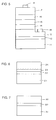
- Fig. 1 is a sectional view showing an exemplary structure of a compound semiconductor light emitting device according to the present invention.
- a light emitting layer 4 consisting of In 0.2 Ga 0.8 N and a clad layer 5 consisting of p-type GaN are successively formed on an epitaxial wafer formed by a GaAs substrate 1, a buffer layer 2 consisting of GaN which is formed on the substrate 1, and an epitaxial layer 3 consisting of cubic n-type GaN which is formed on the buffer layer 2 in this blue light emitting device.
- Electrodes 6 and 7 are formed on an upper part of the clad layer 5 and a rear surface of the substrate 1 respectively.
- an incommensurate plane 8 is located on the interface between the buffer layer 2 and the epitaxial layer 3.
- Fig. 2 schematically illustrates the structure of a vapor phase epitaxy device which is employed for preparing an epitaxial wafer through organic metal chloride vapor phase epitaxy according to the present invention.
- this device is formed by a reaction chamber 54 having first and second gas inlet ports 51 and 52 and an exhaust port 53, and a resistance heater 55 for heating the overall reaction chamber 54 from the exterior.
- a blue light emitting device was prepared in the following manner:
- a gallium arsenide (GaAs) (100) plane substrate 1 which was pretreated with an ordinary H 2 SO 4 etching solution was first set in the reaction chamber 54 of quartz.
- the overall reaction chamber 54 was heated with the resistance heater 55 from the exterior to maintain the substrate 1 at a temperature of 500°C, for introducing trimethylgallium (TMGa) and hydrogen chloride (HCl) as group III raw materials from the first gas inlet port 51 at partial pressures of 8 x 10 -4 atm. and 8 x 10 -4 atm. respectively, while introducing ammonia gas (NH 3 ) as a group V raw material from the second gas inlet port 52 at a partial pressure of 1.6 x 10 -1 atm. Under such conditions, epitaxy was made for 15 minutes, thereby forming a buffer layer 2 consisting of n-type GaN having a thickness of 30 nm. Due to such interposition of the buffer layer 2, it was possible to remarkably improve crystallinity of an epitaxial layer which was formed thereon.
- TMGa trimethylgallium
- HCl hydrogen chloride
- the temperature of the substrate 1 which was provided with the buffer layer 2 consisting of n-type GaN was increased by the resistance heater 55 to 750°C to 800°C, and thereafter epitaxy was made for 60 minutes under such conditions that partial pressures of TMGa, HCl and NH 3 were 8 x 10 -4 atm., 8 x 10 -4 atm. and 1.6 x 10 -1 atm. respectively.
- the temperature of the substrate 1 which was provided with the buffer layer 2 and the epitaxial layer 3 was reduced to the range of 500°C to 700°C by the resistance heater 55, TMGa, trimethylindium (TMIn), HCl and NH 3 were introduced under such conditions that the partial pressure of TMiN was 10 times that of TMGa, and epitaxy was made for 10 minutes.
- a light emitting layer 4 consisting of In 0.2 Ga 0.8 N was formed on the epitaxial layer 3.
- the dopant for the n-type GaN layer was prepared from Si or S, and that for the p-type GaN layer was prepared from Mg. Further, the dopant for the n-type InGaN layer was prepared from Si or S, and that for the n-type InGaN layer was prepared from Zn.
- electrodes 6 and 7 were formed on the clad layer 5 and on the rear surface of the substrate 1 respectively, thereby completing a blue light emitting device.
- a light emitting layer 4 consisting of In 0.5 Ga 0.5 N was formed under the same conditions.
- the light emitting layer was not doped. Consequently, a blue light emitting device having superior wavelength purity to the aforementioned device provided with the light emitting layer of In 0.2 Ga 0.8 N was obtained.
- TMIn When the partial pressure of TMIn was adjusted to be 50 times that of TMGa and the substrate temperature was adjusted in the range of 450°C to 650°C, a light emitting layer 4 consisting of In 0.8 Ga 0.2 N was formed under the same conditions. In 0.8 Ga 0.2 N was not doped. Consequently, a green light emitting device having excellent wavelength purity was obtained.
- a buffer layer 2 consisting of n-type GaN having a thickness of 30 nm was formed on a GaAs (100) plane substrate 1.
- the temperature of the substrate 1 provided with the buffer layer 2 was increased in the range of 800°C to 850°C by the resistance heater 55, and thereafter TMGa, trimethylaluminum (TMAl), HCl and NH 3 were introduced so that TMGa and TMAl were at equal partial pressure ratios to each other, for making epitaxy for 10 minutes.
- TMGa trimethylaluminum
- TMAl trimethylaluminum
- an epitaxial layer 3 consisting of n-type Al 0.1 Ga 0.9 N was formed on the buffer layer 2.
- the temperature of the substrate 1 provided with the buffer layer 2 and the epitaxial layer 3 was reduced in the range of 500°C to 700°C by the resistance heater 55, and thereafter TMGa, TMIn, HCl and NH 3 were introduced so that the partial pressure of TMIn was 10 times that of TMGa, for making epitaxy for 10 minutes.
- a light emitting layer 4 consisting of In 0.2 Ga 0.8 N was formed on the epitaxial layer 3.
- the dopant for the n-type AlGaN layer was prepared from Si or S, and that for the p-type AlGaN layer was prepared from Mg. Further, the dopant for the n-type InGaN layer was prepared from Si or S, and that for the n-type InGaN layer was prepared from Zn.
- electrodes 6 and 7 were formed on the clad layer 5 and on the rear surface of the substrate 1 respectively, thereby completing a blue light emitting device.
- a light emitting layer 4 consisting of In 0.5 Ga 0.5 N was formed under the same conditions.
- the light emitting layer was not doped. Consequently, a blue light emitting device having superior wavelength purity to the device provided with the light emitting layer of In 0.2 Ga 0.8 N was obtained.
- TMIn When the partial pressure of TMIn was adjusted to be 50 times that of TMGa and the substrate temperature was adjusted in the range of 450°C to 650°C, a light emitting layer 4 consisting of In 0.8 Ga 0.2 N was formed under the same conditions. In 0.8 Ga 0.2 N was not doped. Consequently, a green light emitting device having excellent wavelength purity was obtained.
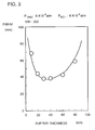
- GaN buffer layers of various thicknesses were formed on GaAs substrates, and GaN epitaxial layers were grown thereon for measuring characteristics of the obtained GaN epitaxial layers.
- the GaN buffer layers and the GaN epitaxial layers were grown under conditions similar to those of Example 1.
- Fig. 3 illustrates the relations between the thicknesses of the GaN buffer layers and full width half maximums (FWHM) of X-ray peaks of the GaN epitaxial layers.
- the axis of abscissas shows the thicknesses (nm) of the GaN buffer layers
- the axis of ordinates shows the full width half maximums (FWHM) (min.) of the X-ray peaks.
- Fig. 4 illustrates the relations between the thicknesses of the GaN buffer layers and the surface irregularities of the GaN epitaxial layers.
- the axis of abscissas shows the thicknesses (nm) of the GaN buffer layers
- the axis of ordinates shows the surface irregularities ( ⁇ m).
- the surface irregularities are defined by the differences between uppermost points of convex portions and lowermost points of concave portions.
- the thickness of the GaN buffer layer is preferably 10 pm to 80 nm, and more preferably 20 nm to 60 nm.
- TMGa triethylgallium
- a compound semiconductor light emitting device was prepared similarly to Example 1, by employing Mg as a dopant for an InGaN layer in place of Si, S or Zn. Other preparation conditions were absolutely similar to those of Example 1, and hence redundant description is omitted.
- This violet light emitting device is absolutely similar in structure to Example 1 shown in Fig. 1 except that the light emitting layer 4 consists of In 0.2 Ga 0.8 N which is doped with Mg, and hence redundant description is omitted.
- TMIn When the partial pressure of TMIn was adjusted to be 50 times that of TMGa and the substrate temperature was adjusted in the range of 450°C to 650°C, a light emitting layer 4 consisting of In 0.8 Ga 0.2 N doped with Mg was formed under the same conditions. Consequently, it was confirmed that a green light emitting device of high performance was obtained.
- a compound semiconductor light emitting device was prepared similarly to Example 2, by employing Mg as a dopant for an InGaN layer in place of Si, S or Zn. At the time of growing a light emitting layer consisting of InGaN, TMGa, TMIn, HCl and NH 3 were introduced so that the partial pressure of IMIn was 20 times that of TMGa. Other preparation conditions were absolutely similar to those of Example 2, and hence redundant description is omitted.
- TMIn When the partial pressure of TMIn was adjusted to be 50 times that of TMGa in the InGaN layer and the substrate temperature was adjusted in the range of 450°C to 650°C, a light emitting layer 4 consisting of In 0.8 Ga 0.2 N doped with Mg was formed under the same conditions. Consequently, it was confirmed that a green light emitting device of high performance was obtained.
- a compound semiconductor light emitting device of high performance can be readily prepared with a substrate of GaAs, GaP, InAs or InP at a low cost.
- band-edge emission can be implemented by Mg doping, whereby wide-ranging application to a laser diode etc. is enabled.
- the method according to the present invention is sufficiently applicable to industrial production.
Landscapes
- Led Devices (AREA)
Applications Claiming Priority (4)
| Application Number | Priority Date | Filing Date | Title |
|---|---|---|---|
| JP6804795A JPH08264835A (ja) | 1995-03-27 | 1995-03-27 | 化合物半導体発光素子およびその製造方法 |
| JP68047/95 | 1995-03-27 | ||
| JP6805195A JPH08264836A (ja) | 1995-03-27 | 1995-03-27 | 化合物半導体発光素子およびその製造方法 |
| JP68051/95 | 1995-03-27 |
Publications (2)
| Publication Number | Publication Date |
|---|---|
| EP0735598A2 true EP0735598A2 (fr) | 1996-10-02 |
| EP0735598A3 EP0735598A3 (fr) | 1998-09-23 |
Family
ID=26409291
Family Applications (1)
| Application Number | Title | Priority Date | Filing Date |
|---|---|---|---|
| EP96103584A Withdrawn EP0735598A3 (fr) | 1995-03-27 | 1996-03-07 | Dispositif émetteur de lumière à composé semi-conducteur et méthode de fabrication |
Country Status (6)
| Country | Link |
|---|---|
| US (2) | US5665986A (fr) |
| EP (1) | EP0735598A3 (fr) |
| KR (1) | KR960036160A (fr) |
| CN (1) | CN1082255C (fr) |
| CA (1) | CA2170922C (fr) |
| TW (1) | TW290743B (fr) |
Cited By (2)
| Publication number | Priority date | Publication date | Assignee | Title |
|---|---|---|---|---|
| DE19725900C2 (de) * | 1997-06-13 | 2003-03-06 | Dieter Bimberg | Verfahren zur Abscheidung von Galliumnitrid auf Silizium-Substraten |
| CN106328771A (zh) * | 2015-07-04 | 2017-01-11 | 东莞市中镓半导体科技有限公司 | 一种在金属氮化镓复合衬底上外延无裂纹高晶体质量led外延层的方法 |
Families Citing this family (27)
| Publication number | Priority date | Publication date | Assignee | Title |
|---|---|---|---|---|
| US5909040A (en) * | 1994-03-09 | 1999-06-01 | Kabushiki Kaisha Toshiba | Semiconductor device including quaternary buffer layer with pinholes |
| JP3771952B2 (ja) * | 1995-06-28 | 2006-05-10 | ソニー株式会社 | 単結晶iii−v族化合物半導体層の成長方法、発光素子の製造方法およびトランジスタの製造方法 |
| JPH0983017A (ja) * | 1995-09-08 | 1997-03-28 | Sumitomo Electric Ind Ltd | エピタキシャルウェハおよびその製造方法 |
| JP2925004B2 (ja) * | 1996-03-22 | 1999-07-26 | 日本電気株式会社 | 窒化ガリウムの結晶成長方法 |
| JP3164016B2 (ja) * | 1996-05-31 | 2001-05-08 | 住友電気工業株式会社 | 発光素子および発光素子用ウエハの製造方法 |
| US6030848A (en) * | 1996-06-28 | 2000-02-29 | Kabushiki Kaisha Toshiba | Method for manufacturing a GaN-based compound semiconductor light emitting device |
| US5684309A (en) * | 1996-07-11 | 1997-11-04 | North Carolina State University | Stacked quantum well aluminum indium gallium nitride light emitting diodes |
| JPH111399A (ja) * | 1996-12-05 | 1999-01-06 | Lg Electron Inc | 窒化ガリウム半導体単結晶基板の製造方法並びにその基板を用いた窒化ガリウムダイオード |
| US6091083A (en) * | 1997-06-02 | 2000-07-18 | Sharp Kabushiki Kaisha | Gallium nitride type compound semiconductor light-emitting device having buffer layer with non-flat surface |
| US6559467B2 (en) * | 1997-11-18 | 2003-05-06 | Technologies And Devices International, Inc. | P-n heterojunction-based structures utilizing HVPE grown III-V compound layers |
| JP4166885B2 (ja) | 1998-05-18 | 2008-10-15 | 富士通株式会社 | 光半導体装置およびその製造方法 |
| US6194742B1 (en) | 1998-06-05 | 2001-02-27 | Lumileds Lighting, U.S., Llc | Strain engineered and impurity controlled III-V nitride semiconductor films and optoelectronic devices |
| KR100495215B1 (ko) * | 2002-12-27 | 2005-06-14 | 삼성전기주식회사 | 수직구조 갈륨나이트라이드 발광다이오드 및 그 제조방법 |
| JP3841092B2 (ja) | 2003-08-26 | 2006-11-01 | 住友電気工業株式会社 | 発光装置 |
| JP2005191530A (ja) * | 2003-12-03 | 2005-07-14 | Sumitomo Electric Ind Ltd | 発光装置 |
| WO2005106985A2 (fr) * | 2004-04-22 | 2005-11-10 | Cree, Inc. | Structure tampon pour substrat amelioree pour dispositifs de nitrure du groupe iii |
| JP2008545266A (ja) * | 2005-07-06 | 2008-12-11 | エルジー イノテック カンパニー リミテッド | 窒化物半導体led及びその製造方法 |
| CN101656288B (zh) * | 2005-07-06 | 2013-06-12 | Lg伊诺特有限公司 | 氮化物半导体led |
| US7585769B2 (en) * | 2006-05-05 | 2009-09-08 | Applied Materials, Inc. | Parasitic particle suppression in growth of III-V nitride films using MOCVD and HVPE |
| TWI309439B (en) * | 2006-09-05 | 2009-05-01 | Ind Tech Res Inst | Nitride semiconductor and method for forming the same |
| US9064706B2 (en) * | 2006-11-17 | 2015-06-23 | Sumitomo Electric Industries, Ltd. | Composite of III-nitride crystal on laterally stacked substrates |
| US20100025796A1 (en) * | 2008-08-04 | 2010-02-04 | Amir Massoud Dabiran | Microchannel plate photocathode |
| JP5378829B2 (ja) * | 2009-02-19 | 2013-12-25 | 住友電気工業株式会社 | エピタキシャルウエハを形成する方法、及び半導体素子を作製する方法 |
| WO2011125290A1 (fr) * | 2010-04-02 | 2011-10-13 | パナソニック株式会社 | Élément semi-conducteur de nitrure et procédé de fabrication de celui-ci |
| DE102011002146B4 (de) * | 2011-04-18 | 2023-03-09 | Aixtron Se | Vorrichtung und Verfahren zum Abscheiden von Halbleiterschichten mit HCI-Zugabe zur Unterdrückung parasitären Wachstums |
| DE102011002145B4 (de) * | 2011-04-18 | 2023-02-09 | Aixtron Se | Vorrichtung und Verfahren zum großflächigen Abscheiden von Halbleiterschichten mit gasgetrennter HCI-Einspeisung |
| CN103258722A (zh) * | 2013-04-27 | 2013-08-21 | 中国电子科技集团公司第十三研究所 | GaAs衬底采用AlGaInN缓冲层生长三族氮化物的方法 |
Family Cites Families (11)
| Publication number | Priority date | Publication date | Assignee | Title |
|---|---|---|---|---|
| US5218216A (en) * | 1987-01-31 | 1993-06-08 | Toyoda Gosei Co., Ltd. | Gallium nitride group semiconductor and light emitting diode comprising it and the process of producing the same |
| US5278433A (en) * | 1990-02-28 | 1994-01-11 | Toyoda Gosei Co., Ltd. | Light-emitting semiconductor device using gallium nitride group compound with double layer structures for the n-layer and/or the i-layer |
| US5281830A (en) * | 1990-10-27 | 1994-01-25 | Toyoda Gosei Co., Ltd. | Light-emitting semiconductor device using gallium nitride group compound |
| JPH088217B2 (ja) * | 1991-01-31 | 1996-01-29 | 日亜化学工業株式会社 | 窒化ガリウム系化合物半導体の結晶成長方法 |
| DE69229265T2 (de) * | 1991-03-18 | 1999-09-23 | Trustees Of Boston University, Boston | Verfahren zur herstellung und dotierung hochisolierender dünner schichten aus monokristallinem galliumnitrid |
| EP0548368A4 (en) * | 1991-07-05 | 1994-10-19 | Mitsubishi Chem Ind | Compound semiconductor and manufacturing method therefor |
| JP2666228B2 (ja) * | 1991-10-30 | 1997-10-22 | 豊田合成株式会社 | 窒化ガリウム系化合物半導体発光素子 |
| US5400740A (en) * | 1992-02-06 | 1995-03-28 | Mitsubishi Chemical Corporation | Method of preparing compound semiconductor |
| JP3247437B2 (ja) * | 1992-03-10 | 2002-01-15 | 旭化成株式会社 | 窒化物系半導体素子およびその製造方法 |
| US5578839A (en) * | 1992-11-20 | 1996-11-26 | Nichia Chemical Industries, Ltd. | Light-emitting gallium nitride-based compound semiconductor device |
| US5523589A (en) * | 1994-09-20 | 1996-06-04 | Cree Research, Inc. | Vertical geometry light emitting diode with group III nitride active layer and extended lifetime |
-
1996
- 1996-02-23 TW TW085102056A patent/TW290743B/zh not_active IP Right Cessation
- 1996-03-04 CA CA002170922A patent/CA2170922C/fr not_active Expired - Fee Related
- 1996-03-07 EP EP96103584A patent/EP0735598A3/fr not_active Withdrawn
- 1996-03-07 US US08/614,837 patent/US5665986A/en not_active Expired - Lifetime
- 1996-03-12 KR KR1019960006429A patent/KR960036160A/ko not_active Ceased
- 1996-03-27 CN CN96104423A patent/CN1082255C/zh not_active Expired - Fee Related
-
1997
- 1997-05-15 US US08/856,911 patent/US5756374A/en not_active Expired - Lifetime
Cited By (3)
| Publication number | Priority date | Publication date | Assignee | Title |
|---|---|---|---|---|
| DE19725900C2 (de) * | 1997-06-13 | 2003-03-06 | Dieter Bimberg | Verfahren zur Abscheidung von Galliumnitrid auf Silizium-Substraten |
| CN106328771A (zh) * | 2015-07-04 | 2017-01-11 | 东莞市中镓半导体科技有限公司 | 一种在金属氮化镓复合衬底上外延无裂纹高晶体质量led外延层的方法 |
| CN106328771B (zh) * | 2015-07-04 | 2018-08-17 | 东莞市中镓半导体科技有限公司 | 一种在金属氮化镓复合衬底上外延无裂纹高晶体质量led外延层的方法 |
Also Published As
| Publication number | Publication date |
|---|---|
| CA2170922A1 (fr) | 1996-09-28 |
| CN1082255C (zh) | 2002-04-03 |
| US5665986A (en) | 1997-09-09 |
| US5756374A (en) | 1998-05-26 |
| CA2170922C (fr) | 2000-02-01 |
| EP0735598A3 (fr) | 1998-09-23 |
| KR960036160A (ko) | 1996-10-28 |
| TW290743B (fr) | 1996-11-11 |
| CN1137690A (zh) | 1996-12-11 |
Similar Documents
| Publication | Publication Date | Title |
|---|---|---|
| US5756374A (en) | Compound semiconductor light emitting device and method of preparing the same | |
| US5843590A (en) | Epitaxial wafer and method of preparing the same | |
| JP5792209B2 (ja) | 有機金属化学気相成長法による、高品質のN面GaN、InNおよびAlNならびにそれらの合金のヘテロエピタキシャル成長の方法 | |
| US5006908A (en) | Epitaxial Wurtzite growth structure for semiconductor light-emitting device | |
| US7655090B2 (en) | Method of controlling stress in gallium nitride films deposited on substrates | |
| US7998773B2 (en) | Method of growing semiconductor heterostructures based on gallium nitride | |
| US6146916A (en) | Method for forming a GaN-based semiconductor light emitting device | |
| US6420283B1 (en) | methods for producing compound semiconductor substrates and light emitting elements | |
| EP0865088B1 (fr) | Procédé de fabrication d'une plaquette epitaxiale comprenant une couche épitaxiale de GaN sur un substrat de GaAs | |
| US20110003420A1 (en) | Fabrication method of gallium nitride-based compound semiconductor | |
| JP3279528B2 (ja) | 窒化物系iii−v族化合物半導体の製造方法 | |
| US6648966B2 (en) | Wafer produced thereby, and associated methods and devices using the wafer | |
| KR20040016724A (ko) | 질화물 반도체 및 그 제조방법 | |
| JPH11135889A (ja) | 結晶成長用基板及びそれを用いた発光装置 | |
| US5864573A (en) | Epitaxial wafer and compound semiconductor light emitting device, and method of fabricating the same | |
| KR100571225B1 (ko) | 질화물계 화합물 반도체의 성장방법 | |
| US6031252A (en) | Epitaxial wafer and method of preparing the same | |
| JPH08293625A (ja) | 三原色発光素子およびその製造方法 | |
| JP3743013B2 (ja) | エピタキシャルウェハの製造方法 | |
| JPH08264835A (ja) | 化合物半導体発光素子およびその製造方法 | |
| JPH08264836A (ja) | 化合物半導体発光素子およびその製造方法 | |
| JPH08264886A (ja) | 半導体レーザ素子およびその製造方法 | |
| JPH08264829A (ja) | 化合物半導体構造およびその製造方法 | |
| JPH08188498A (ja) | エピタキシャルウェハおよびその製造方法 | |
| JP2853631B2 (ja) | 窒化ガリウム単結晶薄膜の製造方法 |
Legal Events
| Date | Code | Title | Description |
|---|---|---|---|
| PUAI | Public reference made under article 153(3) epc to a published international application that has entered the european phase |
Free format text: ORIGINAL CODE: 0009012 |
|
| AK | Designated contracting states |
Kind code of ref document: A2 Designated state(s): DE FR GB |
|
| PUAL | Search report despatched |
Free format text: ORIGINAL CODE: 0009013 |
|
| AK | Designated contracting states |
Kind code of ref document: A3 Designated state(s): DE FR GB |
|
| 17P | Request for examination filed |
Effective date: 19981102 |
|
| 17Q | First examination report despatched |
Effective date: 20040809 |
|
| STAA | Information on the status of an ep patent application or granted ep patent |
Free format text: STATUS: THE APPLICATION IS DEEMED TO BE WITHDRAWN |
|
| 18D | Application deemed to be withdrawn |
Effective date: 20060104 |