EP0735676A1 - Vortreiberschaltung für Hochstromlasten - Google Patents
Vortreiberschaltung für Hochstromlasten Download PDFInfo
- Publication number
- EP0735676A1 EP0735676A1 EP95305642A EP95305642A EP0735676A1 EP 0735676 A1 EP0735676 A1 EP 0735676A1 EP 95305642 A EP95305642 A EP 95305642A EP 95305642 A EP95305642 A EP 95305642A EP 0735676 A1 EP0735676 A1 EP 0735676A1
- Authority
- EP
- European Patent Office
- Prior art keywords
- current
- load
- pull
- circuit
- pull down
- Prior art date
- Legal status (The legal status is an assumption and is not a legal conclusion. Google has not performed a legal analysis and makes no representation as to the accuracy of the status listed.)
- Granted
Links
- 230000008859 change Effects 0.000 claims abstract description 6
- 238000000034 method Methods 0.000 claims description 11
- 230000008569 process Effects 0.000 description 5
- 238000010586 diagram Methods 0.000 description 4
- 239000011159 matrix material Substances 0.000 description 4
- 230000007704 transition Effects 0.000 description 4
- 238000013459 approach Methods 0.000 description 3
- 230000008901 benefit Effects 0.000 description 3
- 230000001965 increasing effect Effects 0.000 description 2
- 238000012986 modification Methods 0.000 description 2
- 230000004048 modification Effects 0.000 description 2
- 230000006978 adaptation Effects 0.000 description 1
- 230000001351 cycling effect Effects 0.000 description 1
- 230000001934 delay Effects 0.000 description 1
- 230000001419 dependent effect Effects 0.000 description 1
- 230000001939 inductive effect Effects 0.000 description 1
- 230000009467 reduction Effects 0.000 description 1
Images


Classifications
-
- H—ELECTRICITY
- H03—ELECTRONIC CIRCUITRY
- H03K—PULSE TECHNIQUE
- H03K17/00—Electronic switching or gating, i.e. not by contact-making and –breaking
- H03K17/16—Modifications for eliminating interference voltages or currents
- H03K17/161—Modifications for eliminating interference voltages or currents in field-effect transistor switches
- H03K17/162—Modifications for eliminating interference voltages or currents in field-effect transistor switches without feedback from the output circuit to the control circuit
- H03K17/163—Soft switching
- H03K17/164—Soft switching using parallel switching arrangements
-
- H—ELECTRICITY
- H03—ELECTRONIC CIRCUITRY
- H03K—PULSE TECHNIQUE
- H03K19/00—Logic circuits, i.e. having at least two inputs acting on one output; Inverting circuits
- H03K19/003—Modifications for increasing the reliability for protection
- H03K19/00346—Modifications for eliminating interference or parasitic voltages or currents
- H03K19/00361—Modifications for eliminating interference or parasitic voltages or currents in field effect transistor circuits
Definitions
- the present invention generally relates to driver circuits for loads which draw a large current (such as light emitting diode drivers) and the reduction of electromagnetic inductance noise emissions caused by high current switching through wires to current loads.
- EMI emissions are considered a hazard and are thus controlled under various standards and government regulations. Therefore, there is a need for devices to control emissions.
- the rate at which the current is being supplied to the load In order to reduce di/dt noise from driving higher current loads, one can control the rate at which the current is being supplied to the load. In general, it is common to slow down the rate at which a driver cycles a heavy current load by providing a predriver circuit sized (that is, chosen to have predetermined operating characteristics) to slow down the rate at which the predriver affects the drive current. However, if the turn on or off rate is high enough to achieve a desired speed of operation, the di/dt noise is also still relatively high. On the other hand, if the predriver turn on or off rate is kept low to reduce noise emissions, it may take too long to drive the load to its new state.
- Anderson switches between two output drivers dependent upon pad noise levels where one driver may be disconnected if the particular application is effected by the increased noise level.
- the present invention provides a current control circuit device for a high current load, having a driver circuit, in a circuit having a power supply and a signal generator for generating a signal to the load.
- the current control circuit device includes: an input connected to the signal generator; an output connected to the driver circuit; a pull up circuit connected between the device input and the output for controlling the rate of current change through the load, having a weak pull up device and a strong pull up device connected in parallel; and a pull down device connected between the device input and output for controlling the rate of current change through the load, having a weak pull down device and a strong pull down device connected in parallel.
- the present invention as shown in FIGURE 1 is adapted to a high current load 101 to control the rate of current switching through a source (PMOS) or sink (NMOS) in order to suppress the noise generated by a current change, di/dt, as the load is cycled, e.g., a matrix of LED indicators in a control panel apparatus in which LED's are selectively turned on and off.
- a matrix of LED indicators in a control panel apparatus in which LED's are selectively turned on and off.
- Each LED has a source driver 103 and a sink driver 105 as would be known in the art.
- the matrix would be adapted to have plurality of addressable column drivers 103 and field drivers 105 to control the selection of LED's to be switched in accordance with predetermined operational user indications, namely by a particular column and field driver set being switched by the control signal.
- a field predriver circuit 107 for the field driver(s) 105 and a column predriver circuit 109 are provided.
- the field predriver circuit 107 of the present invention as shown in FIGURE 1 is shown and detailed in FIGURE 2.
- the implementation is for a pull down NMOS driver 105, or a current sink.
- the control signal for the field select is shown a Vin107 and will generally be, for example, a HIGH (or digital 1) or a LOW (or a digital 0), depending on whether the field driver 105 associated therewith is to be ENABLED or DISABLED, respectively.
- the first path is through the series combination of transistors N1 and N2.
- NMOS transistor N1 is connected between Vout107 with its gate to Vin107, with its drain to Vout, and its source to the drain of N2.
- NMOS transistor N2 is diode connected with its drain to the source of N1 and its source to ground. These transistors are sized to provide a strong pull down.
- the second of the two parallel paths from Vout107 to circuit ground is through transistor N3.
- NMOS transistor N3 is sized to provide a weak pull down.
- Field predriver circuit 107 further includes a half latch connected between Vout107 and the circuit bias voltage supply, Vdd, and a PMOS transistor P1 connected between Vdd and Vout107.
- PMOS transistor P1 has its gate connected to Vin107, its source to Vdd and its drain to Vout107.
- the half latch is formed by inverter 201, having its input coupled to Vout107 an its output coupled to a PMOS transistor P2 at its gate.
- PMOS transistor P2 has its source connected to Vdd and its drain to a source terminal of another PMOS transistor P3.
- PMOS transistor P3 has its gate connected to Vin107 and its drain connected to Vout107.
- the column predriver circuit 105 is shown in FIGURE 3.
- the circuit is equivalent to the field predriver circuit but configured for a PMOS current source, or pull up PMOS column driver 103. As would be known in the art, therefore, it is biased and connected as a pull up circuit.
- Vout109 There are two parallel paths from Vout109 to Vdd.
- One path is through the series combination of P1' and P2'.
- P2' is diode connected and P1 is connected between Vout109 and the drain terminal of P2'.
- a weak pull up transistor P3' is connected between Vout109 and Vdd, only in this configuration a PMOS type.
- a half latch is connected between Vout109 and ground. This half latch is formed by inverter 301 and transistors N2' and N3'. Similarly, a weak pull down is provided in the form of NMOS transistor N1' connected between Vout109 and ground.
- the rate of current through the load when switching between states is controlled.
- the rate at which the current source and sink are turned on and off is controlled to achieve a lower di/dt and, therefore, less EMI noise is generated during current switching.
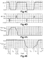
- FIGURE 4A The output voltage of the column predriver 109, Vout109, is plotted in FIGURE 4A.
- the load 101 current is plotted in FIGURE 4C. Note, however, that the di/dt shown in FIGURE 4D is concentrated at time periods t 2 and t 4 of FIGURES 4A and 4B. As such, the goal of the present invention is met.
- Vin107 is generally a HIGH or LOW indicating that a field select line for a matrix of LED's is enabled or disabled.
- Vin107 goes HIGH the gate voltage on transistors N1 and N3 rises, transistors N1 and N3 turn on. and transistor N3 starts conducting since it is sized as a weak pull down.
- transistors N1 and N2 are selected to provide a strong pull down to the load, V L .
- V tn is the threshold voltage of NMOS transistor N2 (namely, the turn-on/turn-off point depending on the direction of the gate swing)
- the current through transistor N2 falls to a very low value.
- the weak pull up transistor P1 causes Vout 107 to rise at a slow rate during an initial turn on period, t 4 .
- the inverter 201 starts to turn on while the weak pull up transistor P1 is controlling.
- the strong pull up formed by transistor P2 and P3 causes Vout 107 to rise at a much faster rate, but not much current is switched.
- Transistors P2 and P3 are sized to get the desired time constant for the latter time period, whereas the threshold voltage of the inverter 201 determines the voltage at which the strong pull-up path starts turning on.
- the bulk of the load current is switched in the region where the gate voltage is varying slowly. This keeps the di/dt noise within the predetermined limits, yet the fast Vout 107 rise gets the driver 105 to a full turn on with a minimal delay.
- Vout 107 swing from rail to rail as in a steady state only if one of them is fully on and the other is fully off.
- FIGURE 4A Operation of the column predriver circuit 109 for a PMOS driver 103, e.g., a current source for a LED or a column is shown in FIGURE 4A.
- transistors P1' and P3' will turn on and transistor P2' starts conducting, providing a strong pull up toward Vdd.
- Transistor N1' and N3' will turn off, allowing Vin 109 to rise.
- the series combination of transistors P1' and P2' will have resistance to Vdd and the parallel combination with P3' will determine the rate at which Vout 109 rises to Vdd, the rate slowing as the driver 103 gate voltage reaches Vdd when current switching is most prominent and hence most di/dt noise is generated.
- the driver 103 gate voltage is tailored to have two different transition rates.
- transistor N1' acts as a weak pull down connection between ground and Vout 109 .
- the weak pull down transistor N1' causes Vout 109 to fall at a initial slow rate (FIGURE 4A, t 4 ).
- the inverter 301 starts turning on and the strong pull down formed by transistors N2 and N3 causes Vout 109 to fall faster than the initial rate (FIGURE 4A, t 5 ).
- the predetermined threshold voltage of the inverter 301 determines the voltage at which the strong pull down pair starts turning on.
- the use of the disclosed combination of weak elements and strong elements provides a scheme where the bulk of current switching occurs when the weak elements are active. This helps keep noise low.
- the strong elements help reduce transition time, but hardly participate in current switching whereas the weak elements participate strongly in the current switching but are slower.
- FIGURES 4A to 4D at times t 2 and t 4 , all the current transition is localized, all di/dt is localized, the gate voltages of the driver have low slopes, and the gate-source voltage is close to the threshold voltage.
- the present invention provides predriver devices for PMOS and NMOS type driver circuits that will reduce the di/dt noise due to high current load switching, yet which will permit driver turn on and turn off times to be kept to an acceptable minimum.
Landscapes
- Physics & Mathematics (AREA)
- Engineering & Computer Science (AREA)
- Computer Hardware Design (AREA)
- Computing Systems (AREA)
- General Engineering & Computer Science (AREA)
- Mathematical Physics (AREA)
- Electronic Switches (AREA)
Applications Claiming Priority (2)
| Application Number | Priority Date | Filing Date | Title |
|---|---|---|---|
| US41242195A | 1995-03-29 | 1995-03-29 | |
| US412421 | 1995-03-29 |
Publications (2)
| Publication Number | Publication Date |
|---|---|
| EP0735676A1 true EP0735676A1 (de) | 1996-10-02 |
| EP0735676B1 EP0735676B1 (de) | 2001-05-23 |
Family
ID=23632898
Family Applications (1)
| Application Number | Title | Priority Date | Filing Date |
|---|---|---|---|
| EP95305642A Expired - Lifetime EP0735676B1 (de) | 1995-03-29 | 1995-08-14 | Vortreiberschaltung zum rauscharmen Schalten hoher Ströme in einer Last |
Country Status (5)
| Country | Link |
|---|---|
| US (1) | US5781045A (de) |
| EP (1) | EP0735676B1 (de) |
| JP (1) | JP3703198B2 (de) |
| KR (1) | KR100392799B1 (de) |
| DE (1) | DE69521028T2 (de) |
Cited By (2)
| Publication number | Priority date | Publication date | Assignee | Title |
|---|---|---|---|---|
| WO2001035532A1 (de) * | 1999-11-11 | 2001-05-17 | Infineon Technologies Ag | Integrierte digitalschaltung und verfahren zu deren betrieb |
| CN104467769A (zh) * | 2014-12-10 | 2015-03-25 | 芯原微电子(上海)有限公司 | 片上开关逐级控制电路及方法、片上信号管脚驱动电路 |
Families Citing this family (22)
| Publication number | Priority date | Publication date | Assignee | Title |
|---|---|---|---|---|
| TW402841B (en) * | 1997-04-24 | 2000-08-21 | Hitachi Ltd | Complementary MOS semiconductor circuit |
| US5905399A (en) * | 1997-06-30 | 1999-05-18 | Sun Microsystems, Inc. | CMOS integrated circuit regulator for reducing power supply noise |
| US6208177B1 (en) * | 1999-05-27 | 2001-03-27 | Lucent Technologies Inc. | Output buffer having immediate onset of gentle state transition |
| US6388475B1 (en) * | 1999-12-29 | 2002-05-14 | Intle Corporation | Voltage tolerant high drive pull-up driver for an I/O buffer |
| US6420905B1 (en) | 2000-09-07 | 2002-07-16 | John Haven Davis | Vented CMOS dynamic logic system |
| US6384654B1 (en) * | 2000-10-17 | 2002-05-07 | Glenn Noufer | High speed circuit of particular utility in delay and phase locked loops |
| JP4212767B2 (ja) * | 2000-12-21 | 2009-01-21 | 旭化成エレクトロニクス株式会社 | 高速電流スイッチ回路および高周波電流源 |
| US6798152B2 (en) * | 2002-08-21 | 2004-09-28 | Freescale Semiconductor, Inc. | Closed loop current control circuit and method thereof |
| JP4576538B2 (ja) * | 2004-05-12 | 2010-11-10 | 国立大学法人 岡山大学 | 多次元のスイッチトポロジーを有する集積回路 |
| US7889609B2 (en) * | 2006-09-26 | 2011-02-15 | Silicon Core Technology, Inc. | Enhanced linearity DVD writing current circuit |
| WO2008085961A1 (en) * | 2007-01-05 | 2008-07-17 | Silicon Core Technology, Inc. | Higher performance dvd writing current circuit |
| JP5158620B2 (ja) * | 2007-02-20 | 2013-03-06 | セイコーエプソン株式会社 | 集積回路装置及び電子機器 |
| US8188769B2 (en) * | 2008-05-09 | 2012-05-29 | Analog Devices, Inc. | Method and apparatus for propagation delay and EMI control |
| US20110140708A1 (en) * | 2009-12-11 | 2011-06-16 | William Henry Lueckenbach | System, method, and apparatus for providing redundant power control using a digital output module |
| US9118322B2 (en) * | 2010-10-12 | 2015-08-25 | Alpha And Omega Semiconductor (Cayman) Ltd | Low leakage dynamic bi-directional body-snatching (LLDBBS) scheme for high speed analog switches |
| US9230671B2 (en) * | 2013-07-05 | 2016-01-05 | Kabushiki Kaisha Toshiba | Output circuit and semiconductor storage device |
| US10985644B1 (en) | 2016-06-25 | 2021-04-20 | Active-Semi, Inc. | Optimized gate driver for low voltage power loss protection system |
| US10090675B1 (en) | 2016-06-25 | 2018-10-02 | Active-Semi, Inc. | Fast settlement of supplement converter for power loss protection system |
| US9705402B1 (en) | 2016-06-25 | 2017-07-11 | Active-Semi, Inc. | Power loss protection integrated circuit |
| US10826480B1 (en) * | 2016-07-01 | 2020-11-03 | Active-Semi, Inc. | Gate driver to decrease EMI with shorter dead-time |
| CN107040245B (zh) * | 2017-05-03 | 2023-08-22 | 深圳市硕亚科技有限公司 | 千安培大电流脉冲信号产生装置及didt测试设备 |
| US11984887B2 (en) * | 2020-10-09 | 2024-05-14 | Metis Microsystems, Llc | Circuits and methods to use energy harvested from transient on-chip data |
Citations (7)
| Publication number | Priority date | Publication date | Assignee | Title |
|---|---|---|---|---|
| US4731553A (en) * | 1986-09-30 | 1988-03-15 | Texas Instruments Incorporated | CMOS output buffer having improved noise characteristics |
| US4820942A (en) * | 1988-01-27 | 1989-04-11 | Advanced Micro Devices, Inc. | High-speed, high-drive output buffer circuits with reduced ground bounce |
| US4825101A (en) * | 1988-02-11 | 1989-04-25 | Advanced Micro Devices, Inc. | Full-level, fast CMOS output buffer |
| EP0315473A2 (de) * | 1987-11-05 | 1989-05-10 | Texas Instruments Incorporated | Ausgangspuffer mit programmierbarem Treiberstrom |
| US5039874A (en) | 1990-03-15 | 1991-08-13 | Hewlett-Packard Company | Method and apparatus for driving an integrated-circuit output pad |
| US5061861A (en) * | 1988-05-20 | 1991-10-29 | Mitsubishi Denki Kabushiki Kaisha | Mos integrated circuit for driving light-emitting diodes |
| US5315173A (en) * | 1991-07-19 | 1994-05-24 | Samsung Electronics Co., Ltd. | Data buffer circuit with delay circuit to increase the length of a switching transition period during data signal inversion |
Family Cites Families (14)
| Publication number | Priority date | Publication date | Assignee | Title |
|---|---|---|---|---|
| US4739198A (en) * | 1985-03-11 | 1988-04-19 | Nec Corporation | Signal output circuit of a push-pull type |
| JPS61292412A (ja) * | 1985-06-20 | 1986-12-23 | Fujitsu Ltd | 出力回路 |
| US4719369A (en) * | 1985-08-14 | 1988-01-12 | Hitachi, Ltd. | Output circuit having transistor monitor for matching output impedance to load impedance |
| US4638187A (en) * | 1985-10-01 | 1987-01-20 | Vtc Incorporated | CMOS output buffer providing high drive current with minimum output signal distortion |
| US4825099A (en) * | 1987-12-04 | 1989-04-25 | Ford Microelectronics | Feedback-controlled current output driver having reduced current surge |
| US5293082A (en) * | 1988-06-21 | 1994-03-08 | Western Digital Corporation | Output driver for reducing transient noise in integrated circuits |
| US4880997A (en) * | 1988-08-18 | 1989-11-14 | Ncr Corporation | Low noise output buffer circuit |
| US4961010A (en) * | 1989-05-19 | 1990-10-02 | National Semiconductor Corporation | Output buffer for reducing switching induced noise |
| JPH0752829B2 (ja) * | 1989-09-13 | 1995-06-05 | 株式会社東芝 | 出力回路 |
| IT1246755B (it) * | 1990-12-28 | 1994-11-26 | Sgs Thomson Microelectronics | Circuito di pilotaggio veloce di un carico capacitivo per circuiti integrari, particolarmente memorie. |
| JP2932722B2 (ja) * | 1991-02-28 | 1999-08-09 | 日本電気株式会社 | 電流駆動回路 |
| US5192881A (en) * | 1991-06-28 | 1993-03-09 | Vlsi Technology, Inc. | Circuit which reduces noise caused by high current outputs |
| US5218239A (en) * | 1991-10-03 | 1993-06-08 | National Semiconductor Corporation | Selectable edge rate cmos output buffer circuit |
| KR940010673B1 (ko) * | 1992-08-24 | 1994-10-24 | 삼성전자 주식회사 | 저전력 데이타 출력버퍼 |
-
1995
- 1995-08-14 DE DE69521028T patent/DE69521028T2/de not_active Expired - Fee Related
- 1995-08-14 EP EP95305642A patent/EP0735676B1/de not_active Expired - Lifetime
-
1996
- 1996-03-25 JP JP06769296A patent/JP3703198B2/ja not_active Expired - Fee Related
- 1996-03-28 KR KR1019960008724A patent/KR100392799B1/ko not_active Expired - Fee Related
- 1996-08-30 US US08/706,377 patent/US5781045A/en not_active Expired - Fee Related
Patent Citations (7)
| Publication number | Priority date | Publication date | Assignee | Title |
|---|---|---|---|---|
| US4731553A (en) * | 1986-09-30 | 1988-03-15 | Texas Instruments Incorporated | CMOS output buffer having improved noise characteristics |
| EP0315473A2 (de) * | 1987-11-05 | 1989-05-10 | Texas Instruments Incorporated | Ausgangspuffer mit programmierbarem Treiberstrom |
| US4820942A (en) * | 1988-01-27 | 1989-04-11 | Advanced Micro Devices, Inc. | High-speed, high-drive output buffer circuits with reduced ground bounce |
| US4825101A (en) * | 1988-02-11 | 1989-04-25 | Advanced Micro Devices, Inc. | Full-level, fast CMOS output buffer |
| US5061861A (en) * | 1988-05-20 | 1991-10-29 | Mitsubishi Denki Kabushiki Kaisha | Mos integrated circuit for driving light-emitting diodes |
| US5039874A (en) | 1990-03-15 | 1991-08-13 | Hewlett-Packard Company | Method and apparatus for driving an integrated-circuit output pad |
| US5315173A (en) * | 1991-07-19 | 1994-05-24 | Samsung Electronics Co., Ltd. | Data buffer circuit with delay circuit to increase the length of a switching transition period during data signal inversion |
Cited By (3)
| Publication number | Priority date | Publication date | Assignee | Title |
|---|---|---|---|---|
| WO2001035532A1 (de) * | 1999-11-11 | 2001-05-17 | Infineon Technologies Ag | Integrierte digitalschaltung und verfahren zu deren betrieb |
| CN104467769A (zh) * | 2014-12-10 | 2015-03-25 | 芯原微电子(上海)有限公司 | 片上开关逐级控制电路及方法、片上信号管脚驱动电路 |
| CN104467769B (zh) * | 2014-12-10 | 2017-12-26 | 芯原微电子(上海)有限公司 | 片上开关逐级控制电路及方法、片上信号管脚驱动电路 |
Also Published As
| Publication number | Publication date |
|---|---|
| JPH08279738A (ja) | 1996-10-22 |
| EP0735676B1 (de) | 2001-05-23 |
| US5781045A (en) | 1998-07-14 |
| KR100392799B1 (ko) | 2003-11-20 |
| DE69521028T2 (de) | 2001-09-06 |
| JP3703198B2 (ja) | 2005-10-05 |
| DE69521028D1 (de) | 2001-06-28 |
Similar Documents
| Publication | Publication Date | Title |
|---|---|---|
| EP0735676B1 (de) | Vortreiberschaltung zum rauscharmen Schalten hoher Ströme in einer Last | |
| US5894238A (en) | Output buffer with static and transient pull-up and pull-down drivers | |
| US6624672B2 (en) | Output buffer with constant switching current | |
| KR950008422B1 (ko) | 집적회로 및 이 회로에 사용하기 적합한 제어수단 | |
| US6466063B2 (en) | Push-pull output buffer with gate voltage feedback loop | |
| US4877980A (en) | Time variant drive circuit for high speed bus driver to limit oscillations or ringing on a bus | |
| US4862018A (en) | Noise reduction for output drivers | |
| US5036222A (en) | Output buffer circuit with output voltage sensing for reducing switching induced noise | |
| EP0212584B1 (de) | Ausgangsschaltung mit Pegelstabilisierung | |
| EP0329285B1 (de) | Ausgangspuffer | |
| US6441653B1 (en) | CMOS output driver with slew rate control | |
| US5128555A (en) | Pulsed CMOS logic circuit having selectable rise and fall times | |
| JP2004266368A (ja) | 半導体装置の駆動方法および装置 | |
| US6664805B2 (en) | Switched capacitor piecewise linear slew rate control methods for output devices | |
| EP0351820B1 (de) | Ausgangschaltung | |
| US6414524B1 (en) | Digital output buffer for MOSFET device | |
| US6356102B1 (en) | Integrated circuit output buffers having control circuits therein that utilize output signal feedback to control pull-up and pull-down time intervals | |
| JP2724331B2 (ja) | Ttl出力ドライバゲート構成 | |
| JPH0514167A (ja) | 出力ドライバ回路 | |
| US4791521A (en) | Method and apparatus for reducing transient noise by premagnetization of parasitic inductance | |
| JP2734398B2 (ja) | 出力バッファ回路 | |
| EP0468209B1 (de) | Pegelumsetzer mit Einzelsteuerung und niedriger dynamischer Impedanz | |
| EP1454414A1 (de) | Schnelle ausgangsschaltung geeignet für geringe spannungen | |
| US6014046A (en) | Off chip driver (OCD) with variable drive capability for noise control | |
| US6100725A (en) | Apparatus for a reduced propagation delay driver |
Legal Events
| Date | Code | Title | Description |
|---|---|---|---|
| PUAI | Public reference made under article 153(3) epc to a published international application that has entered the european phase |
Free format text: ORIGINAL CODE: 0009012 |
|
| AK | Designated contracting states |
Kind code of ref document: A1 Designated state(s): DE FR GB IT |
|
| 17P | Request for examination filed |
Effective date: 19961126 |
|
| 17Q | First examination report despatched |
Effective date: 19990114 |
|
| GRAG | Despatch of communication of intention to grant |
Free format text: ORIGINAL CODE: EPIDOS AGRA |
|
| RIC1 | Information provided on ipc code assigned before grant |
Free format text: 7H 03K 3/01 A, 7H 03K 3/013 B, 7H 03K 19/094 B |
|
| RTI1 | Title (correction) |
Free format text: PREDRIVER CIRCUIT FOR LOW-NOISE SWITCHING OF HIGH CURRENTS IN A LOAD |
|
| RIC1 | Information provided on ipc code assigned before grant |
Free format text: 7H 03K 3/01 A, 7H 03K 3/013 B, 7H 03K 19/094 B |
|
| RTI1 | Title (correction) |
Free format text: PREDRIVER CIRCUIT FOR LOW-NOISE SWITCHING OF HIGH CURRENTS IN A LOAD |
|
| GRAG | Despatch of communication of intention to grant |
Free format text: ORIGINAL CODE: EPIDOS AGRA |
|
| GRAH | Despatch of communication of intention to grant a patent |
Free format text: ORIGINAL CODE: EPIDOS IGRA |
|
| GRAH | Despatch of communication of intention to grant a patent |
Free format text: ORIGINAL CODE: EPIDOS IGRA |
|
| RAP1 | Party data changed (applicant data changed or rights of an application transferred) |
Owner name: HEWLETT-PACKARD COMPANY, A DELAWARE CORPORATION |
|
| RAP1 | Party data changed (applicant data changed or rights of an application transferred) |
Owner name: AGILENT TECHNOLOGIES, INC. |
|
| GRAA | (expected) grant |
Free format text: ORIGINAL CODE: 0009210 |
|
| ITF | It: translation for a ep patent filed | ||
| AK | Designated contracting states |
Kind code of ref document: B1 Designated state(s): DE FR GB IT |
|
| REF | Corresponds to: |
Ref document number: 69521028 Country of ref document: DE Date of ref document: 20010628 |
|
| PGFP | Annual fee paid to national office [announced via postgrant information from national office to epo] |
Ref country code: FR Payment date: 20010718 Year of fee payment: 7 |
|
| RAP2 | Party data changed (patent owner data changed or rights of a patent transferred) |
Owner name: AGILENT TECHNOLOGIES INC. |
|
| RAP2 | Party data changed (patent owner data changed or rights of a patent transferred) |
Owner name: AGILENT TECHNOLOGIES INC. A DELAWARE CORPORATION |
|
| ET | Fr: translation filed | ||
| RAP2 | Party data changed (patent owner data changed or rights of a patent transferred) |
Owner name: AGILENT TECHNOLOGIES, INC. (A DELAWARE CORPORATION |
|
| REG | Reference to a national code |
Ref country code: GB Ref legal event code: IF02 |
|
| PLBE | No opposition filed within time limit |
Free format text: ORIGINAL CODE: 0009261 |
|
| STAA | Information on the status of an ep patent application or granted ep patent |
Free format text: STATUS: NO OPPOSITION FILED WITHIN TIME LIMIT |
|
| 26N | No opposition filed | ||
| PGFP | Annual fee paid to national office [announced via postgrant information from national office to epo] |
Ref country code: DE Payment date: 20020830 Year of fee payment: 8 |
|
| PG25 | Lapsed in a contracting state [announced via postgrant information from national office to epo] |
Ref country code: FR Free format text: LAPSE BECAUSE OF NON-PAYMENT OF DUE FEES Effective date: 20030430 |
|
| REG | Reference to a national code |
Ref country code: FR Ref legal event code: ST |
|
| PG25 | Lapsed in a contracting state [announced via postgrant information from national office to epo] |
Ref country code: DE Free format text: LAPSE BECAUSE OF NON-PAYMENT OF DUE FEES Effective date: 20040302 |
|
| PG25 | Lapsed in a contracting state [announced via postgrant information from national office to epo] |
Ref country code: IT Free format text: LAPSE BECAUSE OF NON-PAYMENT OF DUE FEES Effective date: 20050814 |
|
| REG | Reference to a national code |
Ref country code: GB Ref legal event code: 732E |
|
| PGFP | Annual fee paid to national office [announced via postgrant information from national office to epo] |
Ref country code: GB Payment date: 20060825 Year of fee payment: 12 |
|
| GBPC | Gb: european patent ceased through non-payment of renewal fee |
Effective date: 20070814 |
|
| PG25 | Lapsed in a contracting state [announced via postgrant information from national office to epo] |
Ref country code: GB Free format text: LAPSE BECAUSE OF NON-PAYMENT OF DUE FEES Effective date: 20070814 |