EP0735689B1 - Monolithisch integrierte spannungsgesteuerte Oszillatorschaltung - Google Patents
Monolithisch integrierte spannungsgesteuerte Oszillatorschaltung Download PDFInfo
- Publication number
- EP0735689B1 EP0735689B1 EP96103410A EP96103410A EP0735689B1 EP 0735689 B1 EP0735689 B1 EP 0735689B1 EP 96103410 A EP96103410 A EP 96103410A EP 96103410 A EP96103410 A EP 96103410A EP 0735689 B1 EP0735689 B1 EP 0735689B1
- Authority
- EP
- European Patent Office
- Prior art keywords
- oscillator
- voltage controlled
- controlled oscillator
- vco
- frequency
- Prior art date
- Legal status (The legal status is an assumption and is not a legal conclusion. Google has not performed a legal analysis and makes no representation as to the accuracy of the status listed.)
- Expired - Lifetime
Links
- 230000010355 oscillation Effects 0.000 claims description 4
- 230000001419 dependent effect Effects 0.000 abstract description 3
- 230000003019 stabilising effect Effects 0.000 abstract 1
- 238000004519 manufacturing process Methods 0.000 description 3
- 238000010586 diagram Methods 0.000 description 2
- 238000011084 recovery Methods 0.000 description 2
- 238000010009 beating Methods 0.000 description 1
- 239000003990 capacitor Substances 0.000 description 1
- 238000005516 engineering process Methods 0.000 description 1
- 230000002787 reinforcement Effects 0.000 description 1
- 239000004065 semiconductor Substances 0.000 description 1
- 208000024891 symptom Diseases 0.000 description 1
Images


Classifications
-
- H—ELECTRICITY
- H03—ELECTRONIC CIRCUITRY
- H03L—AUTOMATIC CONTROL, STARTING, SYNCHRONISATION OR STABILISATION OF GENERATORS OF ELECTRONIC OSCILLATIONS OR PULSES
- H03L1/00—Stabilisation of generator output against variations of physical values, e.g. power supply
-
- H—ELECTRICITY
- H03—ELECTRONIC CIRCUITRY
- H03K—PULSE TECHNIQUE
- H03K3/00—Circuits for generating electric pulses; Monostable, bistable or multistable circuits
- H03K3/01—Details
- H03K3/011—Modifications of generator to compensate for variations in physical values, e.g. voltage, temperature
-
- H—ELECTRICITY
- H03—ELECTRONIC CIRCUITRY
- H03L—AUTOMATIC CONTROL, STARTING, SYNCHRONISATION OR STABILISATION OF GENERATORS OF ELECTRONIC OSCILLATIONS OR PULSES
- H03L1/00—Stabilisation of generator output against variations of physical values, e.g. power supply
- H03L1/02—Stabilisation of generator output against variations of physical values, e.g. power supply against variations of temperature only
- H03L1/022—Stabilisation of generator output against variations of physical values, e.g. power supply against variations of temperature only by indirect stabilisation, i.e. by generating an electrical correction signal which is a function of the temperature
- H03L1/027—Stabilisation of generator output against variations of physical values, e.g. power supply against variations of temperature only by indirect stabilisation, i.e. by generating an electrical correction signal which is a function of the temperature by using frequency conversion means which is variable with temperature, e.g. mixer, frequency divider, pulse add/subtract logic circuit
Definitions
- Phase detectors as used in phase locked loops (PLLs) for clock recovery from a data signal can be used, provide an output signal that has a phase difference between their two input signals, however is no longer helpful for clock recovery if at the same time the frequency difference between the two input signals of the phase detector is too large. So that the phase locked loop can still snap to the clock frequency, the frequency range of the voltage-controlled Oscillators (VCO) should be as small as possible.
- VCO voltage-controlled Oscillators
- the frequency range of an integrated in ECL technology, voltage controlled oscillator depends heavily on the operating temperature of chips and manufacturing-related variations the semiconductor parameters. To make sure that the Oscillator can vibrate at the desired frequency the tunable frequency range is designed so large that the desired frequency not only in the normal case, but also in worst case can be reached safely; the tuning area must be correspondingly large (greater than an octave) his. Then it is no longer certain that the phase locked loop just snaps into the correct frequency; she could instead be at double frequency, for example click into place.
- US-E RE34,317 already has a monolithically integrated one voltage-controlled oscillator circuit known, at which is a voltage controlled oscillator and an additional, identical oscillator are provided on the same chip. Furthermore, the vibration frequency of the additional Oscillator for temperature or parameter influence on the Oscillator frequency opposite control signal for the voltage controlled oscillator derived.
- the additional control signal is by comparing the vibration frequency of the additional oscillator with the frequency of an integrated, stable reference oscillator in a co-integrated Phase comparator won.
- the invention now shows one way to even less circuit-intensive voltage-controlled oscillator high Accuracy.
- the invention relates to a monolithically integrated voltage-controlled oscillator circuit according to the preamble of claim 1 and according to the invention, characterized in that the additional oscillator but not a voltage controlled one Is oscillator, and that the output of the additional oscillator via a chain connection of a monoflop and one subsequent low pass with an additional control input of the voltage controlled oscillator is connected.
- the invention which is not a reference clock as such served, but only one derived from it Information on the frequency of one in the same way as that voltage controlled oscillator temperature and parameter dependent Makes use of the reference oscillator, the nominal frequencies of the two oscillators also very different can advantageously be simple compensation of parameter or temperature-related frequency deviations of a monolithically integrated voltage controlled Oscillator.
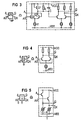
- FIG 1 shows schematically in one for understanding scope of the invention a voltage-controlled voltage control integrated monolithically on a chip Ch Oscillator circuit. It is in addition to the actual voltage controlled oscillator VCO on the same Chip Ch provided a similar oscillator O which is not externally voltage-controlled and its oscillation frequency in basically the same way as that of voltage controlled oscillator VCO from the operating temperature of the chip Ch and the manufacturing parameters.
- FIG. 2 Another circuit-specific details Block diagram of such a monolithically integrated voltage-controlled Oscillator circuit according to the invention shown in FIG.
- the reference oscillator O with an inverting feedback chain connection from Buffer circuits B and level shifters P are formed.
- the actual voltage-controlled is similar Rectangular oscillator VCO with a positive feedback Chain connection of buffer circuits B and level shifters S formed, but here in the derailleur a control element M is also provided for frequency control is.
- a derailleur circuit consisting of monoflop MF, low pass F and Amplifier V.
- the ECL buffer circuits B can be seen in FIG Be realized and ECL level shifter S in the evident from FIG 5; from the level shifters S according to 5 differ the level shifters P only in that that the cross-current sources in them are not controllable are.
- the runtime of an ECL buffer B depends on Cross current of the preceding level shifter P or S from: each the greater the cross current, the smaller (with certain Limits) the term. That can be exploited to the frequency to change the oscillator.
- the monostable flip-flop MF (in FIG 1 and FIG 2) can in the 3 apparent manner can be realized.
- the time-determining Elements of the ECL monoflop MF according to FIG. 3 are the Resistor R and capacitance C. You have to do so be that they are as independent of manufacturing parameters as possible are what e.g. with a large resistance and the Utilization of the capacity between two wiring levels in the Chip can be achieved.
- the transistor Q1 serves the Limit voltage across the RC gate so that the capacitor C is always charged to a defined voltage. The Temperature dependence can be compensated for if necessary by in the monoflop outlined in FIG. 3, the control voltage of the tracks other transistors of the output buffer accordingly, what, without this being explained further here must, by an appropriate temperature-dependent control the associated power source can be reached.
- the voltage-controlled square-wave oscillator VCO (in FIG. 1 and FIG. 2) control element M provided for frequency control can be realized in the manner shown in FIG. 6.
- the frequency-controlling element M is an ECL analog signal multiplexer, whose two inputs A / AX and B / BX in voltage-controlled rectangular oscillator VCO according to FIG 2 two successive level shifters (via a buffer circuit B) S are connected and its control input C / CX the frequency control input of the voltage controlled oscillator VCO (in FIG 1 and FIG 2) forms.
- the between the Control input terminals C and CX supply voltage adjust how much that occurs at input A / AX Signal or the signal occurring at input B / BX on Output Q / QX affects.
Landscapes
- Stabilization Of Oscillater, Synchronisation, Frequency Synthesizers (AREA)
- Inductance-Capacitance Distribution Constants And Capacitance-Resistance Oscillators (AREA)
- Semiconductor Integrated Circuits (AREA)
- Networks Using Active Elements (AREA)
Description
- FIG 1
- ein Blockschaltbild eines Ausführungsbeispiels einer monolithisch integrierten spannungsgesteuerten Oszillatorschaltung gemäß der Erfindung;
- FIG 2 bis FIG 6
- zeigen schaltungstechnische Einzelheiten dazu.
Claims (3)
- Monolithisch integrierte spannungsgesteuerte Oszillatorschaltung, wobei ein spannungsgesteuerter Oszillator (VCO) und ein zusätzlicher, gleichartiger Oszillator (O) auf demselben Chip (Ch) vorgesehen sind, wobei aus der Schwingungsfrequenz des zusätzlichen Oszillators (O) ein zum Temperatur- bzw. Parametereinfluß auf die Oszillatorfrequenz gegensinniges Zusatz-Steuersignal für den spannungsgesteuerten Oszillator abgeleitet wird,
dadurch gekennzeichnet,
daß der zusätzliche Oszillator (O) jedoch kein spannungsgesteuerter Oszillator ist, und daß der Ausgang des zusätzlichen Oszillators (O) über eine Kettenschaltung eines Monoflops (MF) und eines nachfolgenden Tiefpasses (F) mit einem Zusatz-Steuereingang (z) des spannungsgesteuerten Oszillators (VCO) verbunden ist. - Spannungsgesteuerte Oszillatorschaltung nach Anspruch 1,
dadurch gekennzeichnet,
daß die beiden Oszillatoren (O) VCO) jeweils mit einer rückgekoppelten Kettenschaltung von ECL-Bufferschaltungen (B) und ECL-Pegelschiebern (P; S) gebildet sind. - Spannungsgesteuerte Oszillatorschaltung nach Anspruch 2 , dadurch gekennzeichnet,
daß der spannungsgesteuerte Oszillator (VCO) ein spannungsgesteuerter Rechteckoszillator ist; und daß ein im spannungsgesteuerten Rechteckoszillator (VCO) vorgesehenes Steuerglied (M) zur Frequenzsteuerung ein ECL-Analogsignal-Multiplexer ist, dessen beide Eingänge (A/AX, B/BX) an zwei über eine Bufferschaltung (B) aufeinanderfolgende Pegelschieber (S) angeschlossen sind und dessen Steuereingang (C/CX) den Frequenzsteuereingang des spannungsgesteuerten Oszillators (VCO) bildet.
Applications Claiming Priority (2)
| Application Number | Priority Date | Filing Date | Title |
|---|---|---|---|
| DE19511402 | 1995-03-28 | ||
| DE19511402A DE19511402C1 (de) | 1995-03-28 | 1995-03-28 | Monolithisch integrierte spannungsgesteuerte Oszillatorschaltung |
Publications (3)
| Publication Number | Publication Date |
|---|---|
| EP0735689A2 EP0735689A2 (de) | 1996-10-02 |
| EP0735689A3 EP0735689A3 (de) | 1996-12-27 |
| EP0735689B1 true EP0735689B1 (de) | 2000-09-06 |
Family
ID=7757987
Family Applications (1)
| Application Number | Title | Priority Date | Filing Date |
|---|---|---|---|
| EP96103410A Expired - Lifetime EP0735689B1 (de) | 1995-03-28 | 1996-03-05 | Monolithisch integrierte spannungsgesteuerte Oszillatorschaltung |
Country Status (7)
| Country | Link |
|---|---|
| US (1) | US5751196A (de) |
| EP (1) | EP0735689B1 (de) |
| AT (1) | ATE196217T1 (de) |
| CA (1) | CA2172704A1 (de) |
| DE (2) | DE19511402C1 (de) |
| ES (1) | ES2150609T3 (de) |
| RU (1) | RU2108662C1 (de) |
Families Citing this family (3)
| Publication number | Priority date | Publication date | Assignee | Title |
|---|---|---|---|---|
| CN102201785B (zh) * | 2010-03-23 | 2013-06-26 | 北京大学 | 一种超低功耗压控振荡器电路及其信号处理方法 |
| US9698872B2 (en) | 2013-06-18 | 2017-07-04 | Qualcomm Incorporated | Methods and apparatus for improving remote NFC device detection using a low power oscillator circuit |
| US9473151B1 (en) | 2015-06-05 | 2016-10-18 | Telefonaktiebolaget Lm Ericsson (Publ) | Low-noise oscillator amplitude regulator |
Family Cites Families (8)
| Publication number | Priority date | Publication date | Assignee | Title |
|---|---|---|---|---|
| US3713033A (en) * | 1971-09-01 | 1973-01-23 | Collins Radio Co | Digitally temperature compensated oscillator |
| US4492933A (en) * | 1982-07-28 | 1985-01-08 | Motorola, Inc. | Temperature compensation circuit for oscillator with parabolic characteristic |
| USRE34317E (en) * | 1982-08-05 | 1993-07-20 | Seiko Epson Corporation | Variable frequency oscillator |
| FR2548848A1 (fr) * | 1983-07-06 | 1985-01-11 | Thomson Csf | Generateur de frequence compense en temperature |
| DE3341780A1 (de) * | 1983-11-18 | 1985-05-30 | Siemens AG, 1000 Berlin und 8000 München | Anordnung zur stabilisierung der von einem frequenzgenerator, insbesondere einem quarzgenerator, abgegebenen frequenz |
| EP0307595A1 (de) * | 1987-09-11 | 1989-03-22 | Siemens Aktiengesellschaft | Schaltungsanordnung zur Erzeugung zweier eng benachbarter Frequenzen |
| US5357220A (en) * | 1993-01-21 | 1994-10-18 | Gennum Corporation | Emitter-coupled oscillator with differential switching control |
| US5438599A (en) * | 1993-09-30 | 1995-08-01 | Lsi Logic Corporation | Self-calibration timing circuit |
-
1995
- 1995-03-28 DE DE19511402A patent/DE19511402C1/de not_active Expired - Fee Related
-
1996
- 1996-03-05 AT AT96103410T patent/ATE196217T1/de not_active IP Right Cessation
- 1996-03-05 EP EP96103410A patent/EP0735689B1/de not_active Expired - Lifetime
- 1996-03-05 ES ES96103410T patent/ES2150609T3/es not_active Expired - Lifetime
- 1996-03-05 DE DE59605836T patent/DE59605836D1/de not_active Expired - Fee Related
- 1996-03-26 US US08/621,621 patent/US5751196A/en not_active Expired - Fee Related
- 1996-03-26 CA CA002172704A patent/CA2172704A1/en not_active Abandoned
- 1996-03-27 RU RU96105814/09A patent/RU2108662C1/ru not_active IP Right Cessation
Also Published As
| Publication number | Publication date |
|---|---|
| RU2108662C1 (ru) | 1998-04-10 |
| ATE196217T1 (de) | 2000-09-15 |
| EP0735689A2 (de) | 1996-10-02 |
| CA2172704A1 (en) | 1996-09-29 |
| DE19511402C1 (de) | 1996-11-28 |
| ES2150609T3 (es) | 2000-12-01 |
| DE59605836D1 (de) | 2000-10-12 |
| EP0735689A3 (de) | 1996-12-27 |
| US5751196A (en) | 1998-05-12 |
Similar Documents
| Publication | Publication Date | Title |
|---|---|---|
| DE69412306T2 (de) | Temperaturkompensierter Quarzoszillator | |
| DE69312373T2 (de) | Gesteuerter Schwingkreis | |
| DE69120562T2 (de) | Subnanosekunde kalibrierte Verzögerungsleitungsstruktur | |
| DE102007047458B4 (de) | Ringoszillatorschaltung und PLL-Schaltung | |
| DE19882089B4 (de) | Verstärker zur kontinuierlichen schmalbandigen Signalverstärkung mit hohem Verstärkungsfaktor und Verstärkungsverfahren | |
| EP0591750B1 (de) | Verfahren zur Stromeinstellung eines monolithisch integrierten Padtreibers | |
| EP0735678A2 (de) | Monolithisch integrierter Oszillator | |
| EP0208328B1 (de) | Dynamisches Regelungssystem | |
| EP1391030B1 (de) | Spannungsgesteuerte oszillatorschaltung | |
| DE3036785C2 (de) | Oszillatorschaltung | |
| DE102004025545B4 (de) | CMOS LC-Schwingkreis-Oszillator | |
| DE102005028173B4 (de) | Integrierte CMOS-Tastverhältnis-Korrekturschaltung für ein Taktsignal | |
| US4146849A (en) | Voltage controlled oscillator | |
| DE69002344T2 (de) | Spannungskontrollierter emittergekoppelter Multivibrator mit zwei Eingängen. | |
| EP2853029B1 (de) | Schaltungsanordnung und verfahren zum kalibrieren von ansteuersignalen für spannungsgesteuerte oszillatoren | |
| DE19511402C1 (de) | Monolithisch integrierte spannungsgesteuerte Oszillatorschaltung | |
| DE2310314C3 (de) | Regelschaltung zur Erzeugung eines Signals konstanter Frequenz für einen elektronischen Zeitgeber | |
| DE3221888A1 (de) | Elektronisches, beruehrungslos arbeitendes schaltgeraet | |
| EP2862280A2 (de) | Schaltungsanordnung und verfahren zur takt- und/oder datenrückgewinnung | |
| DE3853983T2 (de) | Elektronischer Oszillator. | |
| DE3720501C2 (de) | ||
| DE2700070A1 (de) | Anordnung zur temperaturstabilisierung einer abstimmbaren schaltung | |
| DE3938095A1 (de) | Quarzobertonoszillator | |
| DE10162912B4 (de) | Quarzoszillatorschaltung | |
| EP0393398B1 (de) | Oszillator in CMOS-Technik |
Legal Events
| Date | Code | Title | Description |
|---|---|---|---|
| PUAI | Public reference made under article 153(3) epc to a published international application that has entered the european phase |
Free format text: ORIGINAL CODE: 0009012 |
|
| AK | Designated contracting states |
Kind code of ref document: A2 Designated state(s): AT BE CH DE ES FR GB IT LI NL SE |
|
| PUAL | Search report despatched |
Free format text: ORIGINAL CODE: 0009013 |
|
| AK | Designated contracting states |
Kind code of ref document: A3 Designated state(s): AT BE CH DE ES FR GB IT LI NL SE |
|
| 17P | Request for examination filed |
Effective date: 19970604 |
|
| 17Q | First examination report despatched |
Effective date: 19990709 |
|
| GRAG | Despatch of communication of intention to grant |
Free format text: ORIGINAL CODE: EPIDOS AGRA |
|
| GRAG | Despatch of communication of intention to grant |
Free format text: ORIGINAL CODE: EPIDOS AGRA |
|
| GRAH | Despatch of communication of intention to grant a patent |
Free format text: ORIGINAL CODE: EPIDOS IGRA |
|
| 17Q | First examination report despatched |
Effective date: 19990709 |
|
| GRAH | Despatch of communication of intention to grant a patent |
Free format text: ORIGINAL CODE: EPIDOS IGRA |
|
| GRAA | (expected) grant |
Free format text: ORIGINAL CODE: 0009210 |
|
| AK | Designated contracting states |
Kind code of ref document: B1 Designated state(s): AT BE CH DE ES FR GB IT LI NL SE |
|
| REF | Corresponds to: |
Ref document number: 196217 Country of ref document: AT Date of ref document: 20000915 Kind code of ref document: T |
|
| REG | Reference to a national code |
Ref country code: CH Ref legal event code: NV Representative=s name: SIEMENS SCHWEIZ AG Ref country code: CH Ref legal event code: EP |
|
| REF | Corresponds to: |
Ref document number: 59605836 Country of ref document: DE Date of ref document: 20001012 |
|
| ITF | It: translation for a ep patent filed | ||
| REG | Reference to a national code |
Ref country code: ES Ref legal event code: FG2A Ref document number: 2150609 Country of ref document: ES Kind code of ref document: T3 |
|
| GBT | Gb: translation of ep patent filed (gb section 77(6)(a)/1977) |
Effective date: 20001109 |
|
| ET | Fr: translation filed | ||
| PLBE | No opposition filed within time limit |
Free format text: ORIGINAL CODE: 0009261 |
|
| STAA | Information on the status of an ep patent application or granted ep patent |
Free format text: STATUS: NO OPPOSITION FILED WITHIN TIME LIMIT |
|
| 26N | No opposition filed | ||
| REG | Reference to a national code |
Ref country code: GB Ref legal event code: IF02 |
|
| PGFP | Annual fee paid to national office [announced via postgrant information from national office to epo] |
Ref country code: GB Payment date: 20020305 Year of fee payment: 7 |
|
| PGFP | Annual fee paid to national office [announced via postgrant information from national office to epo] |
Ref country code: NL Payment date: 20020308 Year of fee payment: 7 |
|
| PGFP | Annual fee paid to national office [announced via postgrant information from national office to epo] |
Ref country code: SE Payment date: 20020312 Year of fee payment: 7 |
|
| PGFP | Annual fee paid to national office [announced via postgrant information from national office to epo] |
Ref country code: ES Payment date: 20020321 Year of fee payment: 7 Ref country code: BE Payment date: 20020321 Year of fee payment: 7 |
|
| PGFP | Annual fee paid to national office [announced via postgrant information from national office to epo] |
Ref country code: FR Payment date: 20020326 Year of fee payment: 7 |
|
| PGFP | Annual fee paid to national office [announced via postgrant information from national office to epo] |
Ref country code: DE Payment date: 20020521 Year of fee payment: 7 |
|
| PGFP | Annual fee paid to national office [announced via postgrant information from national office to epo] |
Ref country code: CH Payment date: 20020610 Year of fee payment: 7 |
|
| PGFP | Annual fee paid to national office [announced via postgrant information from national office to epo] |
Ref country code: AT Payment date: 20030212 Year of fee payment: 8 |
|
| PG25 | Lapsed in a contracting state [announced via postgrant information from national office to epo] |
Ref country code: GB Free format text: LAPSE BECAUSE OF NON-PAYMENT OF DUE FEES Effective date: 20030305 |
|
| PG25 | Lapsed in a contracting state [announced via postgrant information from national office to epo] |
Ref country code: SE Free format text: LAPSE BECAUSE OF NON-PAYMENT OF DUE FEES Effective date: 20030306 Ref country code: ES Free format text: LAPSE BECAUSE OF NON-PAYMENT OF DUE FEES Effective date: 20030306 |
|
| PG25 | Lapsed in a contracting state [announced via postgrant information from national office to epo] |
Ref country code: LI Free format text: LAPSE BECAUSE OF NON-PAYMENT OF DUE FEES Effective date: 20030331 Ref country code: CH Free format text: LAPSE BECAUSE OF NON-PAYMENT OF DUE FEES Effective date: 20030331 Ref country code: BE Free format text: LAPSE BECAUSE OF NON-PAYMENT OF DUE FEES Effective date: 20030331 |
|
| BERE | Be: lapsed |
Owner name: *SIEMENS A.G. Effective date: 20030331 |
|
| PG25 | Lapsed in a contracting state [announced via postgrant information from national office to epo] |
Ref country code: NL Free format text: LAPSE BECAUSE OF NON-PAYMENT OF DUE FEES Effective date: 20031001 Ref country code: DE Free format text: LAPSE BECAUSE OF NON-PAYMENT OF DUE FEES Effective date: 20031001 |
|
| GBPC | Gb: european patent ceased through non-payment of renewal fee |
Effective date: 20030305 |
|
| EUG | Se: european patent has lapsed | ||
| REG | Reference to a national code |
Ref country code: CH Ref legal event code: PL |
|
| PG25 | Lapsed in a contracting state [announced via postgrant information from national office to epo] |
Ref country code: FR Free format text: LAPSE BECAUSE OF NON-PAYMENT OF DUE FEES Effective date: 20031127 |
|
| NLV4 | Nl: lapsed or anulled due to non-payment of the annual fee |
Effective date: 20031001 |
|
| REG | Reference to a national code |
Ref country code: FR Ref legal event code: ST |
|
| PG25 | Lapsed in a contracting state [announced via postgrant information from national office to epo] |
Ref country code: AT Free format text: LAPSE BECAUSE OF NON-PAYMENT OF DUE FEES Effective date: 20040305 |
|
| REG | Reference to a national code |
Ref country code: ES Ref legal event code: FD2A Effective date: 20030306 |
|
| PG25 | Lapsed in a contracting state [announced via postgrant information from national office to epo] |
Ref country code: IT Free format text: LAPSE BECAUSE OF NON-PAYMENT OF DUE FEES Effective date: 20050305 |