EP0735694B1 - Kostengünstige integrierbare Vorrichtung zur Verarbeitung elektrischer Signale nach der ARINC-429-Norm - Google Patents
Kostengünstige integrierbare Vorrichtung zur Verarbeitung elektrischer Signale nach der ARINC-429-Norm Download PDFInfo
- Publication number
- EP0735694B1 EP0735694B1 EP96400563A EP96400563A EP0735694B1 EP 0735694 B1 EP0735694 B1 EP 0735694B1 EP 96400563 A EP96400563 A EP 96400563A EP 96400563 A EP96400563 A EP 96400563A EP 0735694 B1 EP0735694 B1 EP 0735694B1
- Authority
- EP
- European Patent Office
- Prior art keywords
- circuit
- correction
- signal
- counting
- analog
- Prior art date
- Legal status (The legal status is an assumption and is not a legal conclusion. Google has not performed a legal analysis and makes no representation as to the accuracy of the status listed.)
- Expired - Lifetime
Links
- 238000012937 correction Methods 0.000 claims description 78
- 239000003990 capacitor Substances 0.000 claims description 29
- 238000001914 filtration Methods 0.000 claims description 15
- 230000006870 function Effects 0.000 claims description 8
- 230000005540 biological transmission Effects 0.000 claims description 7
- 230000000737 periodic effect Effects 0.000 claims description 4
- 230000000630 rising effect Effects 0.000 claims description 4
- 230000001360 synchronised effect Effects 0.000 claims description 2
- 230000001174 ascending effect Effects 0.000 claims 1
- 238000005259 measurement Methods 0.000 description 15
- 235000021183 entrée Nutrition 0.000 description 10
- 238000001514 detection method Methods 0.000 description 4
- 238000010586 diagram Methods 0.000 description 4
- 238000000034 method Methods 0.000 description 4
- 238000009825 accumulation Methods 0.000 description 3
- 230000003071 parasitic effect Effects 0.000 description 2
- RZVHIXYEVGDQDX-UHFFFAOYSA-N 9,10-anthraquinone Chemical compound C1=CC=C2C(=O)C3=CC=CC=C3C(=O)C2=C1 RZVHIXYEVGDQDX-UHFFFAOYSA-N 0.000 description 1
- 241000861223 Issus Species 0.000 description 1
- 238000012550 audit Methods 0.000 description 1
- 238000006243 chemical reaction Methods 0.000 description 1
- 230000003111 delayed effect Effects 0.000 description 1
- 230000000694 effects Effects 0.000 description 1
- 238000010237 hybrid technique Methods 0.000 description 1
- 230000010354 integration Effects 0.000 description 1
- 230000005433 particle physics related processes and functions Effects 0.000 description 1
- 230000002441 reversible effect Effects 0.000 description 1
- 238000005070 sampling Methods 0.000 description 1
- 239000003381 stabilizer Substances 0.000 description 1
- 230000000087 stabilizing effect Effects 0.000 description 1
- 230000001960 triggered effect Effects 0.000 description 1
Images


Classifications
-
- H—ELECTRICITY
- H03—ELECTRONIC CIRCUITRY
- H03M—CODING; DECODING; CODE CONVERSION IN GENERAL
- H03M3/00—Conversion of analogue values to or from differential modulation
Definitions
- the present invention relates to a device for the acquisition and analog / digital signal conversion electric requiring analog formatting, in particular to minimize or even eliminate the effects of radio interference.
- the ARINC 429 standard defines a transmission protocol for digital data via a wired link including a pair of twisted and shielded wires. She is essentially applied to data transmissions between different electronic equipment on board aircraft, these transmissions being effected by modulation in differential voltage between a single transmitter and a plurality of recipients.
- digital data is transmitted to a speed of 12.5 or 100 kilobits per second, thanks to two analog signals H and L applied respectively to the two wires of the link, these two signals being symmetrical relative to a reference voltage close to zero volts.
- a bit at 1 is represented by the signal H by a trapezoid having a constant voltage range close to one maximum voltage of +10 volts, followed by a voltage range close to the reference voltage.
- a bit at 0 is represented by a trapezoid having a range at constant voltage close to a minimum voltage of -10 volts, followed by a voltage range close to the voltage of reference.
- ARINC 429 can have only one transmitter, some flight control devices have several dozen ARINC 429 signal acquisition channels. that these devices have a very high cost and a space that can hardly be reduced by digital electronics techniques.
- the present invention aims to eliminate these drawbacks. To this end, it provides a device for converting an analog transmission signal digital data into a digital signal, involving a sigma-delta type converter.
- the analog circuit consists only of resistors and capacitors. It is therefore purely passive and can therefore be integrated into a passive component of the hybrid type, such as a DIL network, very inexpensive and compact. Furthermore, given the simplicity of the analog circuit, one is assured of the durability of such hybrid circuits. Furthermore, thanks to the processing carried out on the signal downstream of the threshold comparator, it is not necessary to use a high-precision comparator, which makes it possible to replace the analog comparators normally used by a single digital comparator, the circuit filtering and counting to overcome possible drifts at the threshold. A device is thus obtained which is perfectly suited for receiving analog signals for transmitting digital data.
- the output terminals of the analog circuit are arranged so as to minimize the length of links between circuits analog and digital. In this way, the value of the parasitic capacities due to connections and links.
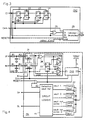
- the digital circuit CN1 comprises a threshold comparator whose input is connected to the input terminal B and to the output of a buffer memory 12.
- This circuit also includes a flip-flop D 13 comprising an input d to which the signal delivered by the threshold comparator 11.
- the signal sent on the output q of the flip-flop 13 is sent to the output SI of the digital circuit CN1, while the inverted output ng of the flip-flop 13 is connected to the input of the buffer memory 12.
- the digital circuit CN1 is clocked by a generator phases 14 designed to provide two synchronous square signals Ckm and According to a clock signal H applied to the input of generator 14, the signal Ckm being applied to the input of the clock signal of the flip-flop D 13, and the signal En to buffer memory 12 to control the state thereof blocked or unlocked and thus validate or not the output.
- the digital circuit CN1 is made in CMOS technology so as to present an impedance high input, when buffer 12 is in the state blocked, and to behave as a source of tension when it is in the unlocked state.
- the signals Ckm and En have a frequency equal to half that of the clock signal H, the signal En with falling flanks in phase with those of the Ckm signal, and rising edges delayed by a quarter of period compared to those of the Ckm signal.
- FIG. 2 also shows the form of the signals at input B and at output SI of the digital circuit CN1, and at input d of the flip-flop D 13, as a function of a signal E applied at the input of the analog circuit CA.
- the shape of the signal d shown in this figure is obtained by means of the comparator 11 which delivers a signal at 0 volts during the periods when the signal at B is below the threshold, and a signal, for example, at + 5 volts during the periods where the voltage at B is above the threshold.
- the signal at B is subjected to remain close to the threshold voltage, the signal at output SI being representative of the corrections made in one direction or the other and applied to the capacitor C.
- the signal SI is used to carry out an accumulation of the corrections over a fixed duration corresponding to N measurement periods, it is possible to evaluate the value of the input voltage which also contributes to changing the voltage across the terminals of the capacitor C through resistor R1.
- An analog / digital converter is thus obtained, the precision of which depends on the period of accumulation of the measurements, on the sampling frequency (Ckm) and of course, on the limitations imposed by the analog characteristics of the elements used by the device according to the invention. It turns out that the precision thus obtained is largely sufficient for the acquisition of ARINC 429 signals.
- FIG. 3 shows a digital filtering circuit CN2 and decimation to perform the accumulation of corrections provided by the output SI of the CN1 circuit on a predetermined period.
- This CN2 circuit includes a shift register consisting of N flip-flops D 21 to 24 connected in series and clocked by the same Ckm signal, the input d of the first flip-flop D 21 constituting the input E1 of this circuit CN2, and being connected to the output SI of the CN1 circuit.
- This CN2 circuit also includes an up / down counter 25 which maintains a balance sheet of the values that enter and come out of the shift register, so as to contain at any instant, with an initialization constant near the number of bits at 1 present in the shift register, this number being representative of the average signal voltage analog applied to input E, over a period corresponding to the N previous measurements, N being the number flip-flops 21 to 24 in the shift register.
- a RESET signal to flip-flops D 21 to 24 of the shift register, alternatively, either on the reset input or on the entry of setting to 1 so as to initialize the register to an average value, for example 0 1 ... 0 1.
- This value mean which corresponds to the initialization value, is also applied to up / down counter 25.
- the value of the up / down counter 25 does not change.
- the value of the up / down counter 25 is incremented, if the signal at the output of the shift register is at logic level 0.
- the value of the up / down counter 25 is decremented, if the input signal E1 is at 0 and if the output of the shift register is at 1.
- the up / down counter 25 is only incremented if a value of 1 replaces a value of 0 in the register at offset, and decremented if a value of 0 replaces a value at 1 in the shift register.
- An ARINC 429 signal in fact comprises two differential signals IP and IM, one being at all times symmetrical with the other with respect to a reference voltage close to zero.
- binary information at 1 is represented on the positive IP channel by a trapezoidal signal having a positive constant voltage range of the order of +10 volts, followed by a constant voltage signal close to the voltage reference, while binary information at 0 is represented by a phase with constant voltage close to - 10 volts followed by a signal with voltage close to the reference voltage.
- the device shown in FIG. 4 comprises two input channels, namely a positive IP channel and a negative IM channel, corresponding to the ARINC 429 signal transmitted in differential over two serial lines. These two inputs are applied to an analog circuit CA2 comprising for each of the inputs, a bridge comprising the resistors R1 and R2 and the capacitor C, as described above.
- This device also includes a digital circuit CN comprising two circuits 31, 32 of the type of the circuit CN1 described above and represented in FIG. 1, the inputs B of these two circuits being connected to the outputs of the analog circuit CA2.
- this device comprises only one CN2 filtering and decimation circuit for two channels analog acquisition.
- it includes a digital circuit CN3 with a door OR EXCLUSIVE 36 whose inputs are connected to the outputs of the circuits CN1 31 and 32.
- This CN3 circuit also includes two selectors 34.35 each having a select input connected to the output of OR EXCLUSIVE door 36, two inputs referenced respectively 0 and 1, and an output which delivers the input signal 0 or 1 selected according to of logic level 0 or 1 respectively, of the signal selection applied to the selection input.
- Input 1 of the first selector 34 is connected to the output q of a D flip-flop 33, while input 0 of this selector is connected to the reverse output nq of the rocker 33, and at input 0 of the other selector 35.
- the output of the first selector 34 is connected to the input d of the rocker 33, which is clocked by the Ckm signal produced by a phase generator such as that referenced 14 on the figure 1.
- the output S1 of the first circuit CN1 31 is by elsewhere applied to input 1 of the second selector 35, whose output is applied to the input E1 of the circuit CN2.
- the respective outputs of the threshold comparators 37 to 40 are applied to the input of a logic circuit 41 designed to generate two logic signals SH and SL shown on FIG. 5, the signal SH containing a pulse for represent each binary information at 1, and the signal SL an impulse to represent each binary information to 0, contained in the IP and IM signals applied as input.
- the logic circuit 41 includes an output of zero threshold detection, indicating whether the reference threshold after a 1 or after a 0 has been crossed, this exit being connected to the entrance of an OR 42 door which is also applied the RESET initialization signal.
- the initialization of rocker D 33 and of the CN2 circuit that is to say, of the shift register 21 to 24 and up / down counter 25 to an average value, to whenever the reference level has been detected in IP and IM input signals.
- resistance R1 is 12 k ⁇
- resistance R2 600 ⁇ is 12 k ⁇
- An ARINC signal being transmitted to the speed of 12.5 or 100 kilobits / second, we use a H clock of 20 MHz so as to obtain a oversampling of the input signal.
- the analog part is extremely small, and can be easily integrated into a DIL network type hybrid circuit.
- the digital part only includes standard functions which can therefore easily be integrated into a integrated digital circuit. It is desirable to have the connection pins B of the digital circuit CN in look at the connection pins of the analog circuit, so as to remove the links between these two circuits and thus to minimize parasitic capacities resulting from these links.
- ARINC 429 channels can be used simultaneously a single phase generator for all channels, condition of timing the measurement and correction phases in phase opposition for groups of two tracks, so as to distribute the current calls over time supplied by the circuit supply, and thus, minimize the amplitude.
Landscapes
- Engineering & Computer Science (AREA)
- Theoretical Computer Science (AREA)
- Analogue/Digital Conversion (AREA)
Claims (11)
- Vorrichtung für die Umwandlung eines analogen Signals für die Übertragung von digitalen Daten in ein digitales Signal, mit:dadurch gekennzeichnet, dass der analoge Schaltkreis (CA) folgendes beinhaltet:einem rein passiven Schaltkreis (CA), an den das empfangene analoge Signal angelegt wird, wobei dieser Schaltkreis einen Kondensator (C) beinhaltet, der von dem empfangenen analogen Signal aufgeladen wird, und eine Verbindungsklemme (B),einem Komparator (11) mit Schwellenwert, um die Spannung an den Anschlussklemmen des Kondensators (C) mit einem Schwellenwert zu vergleichen und ein analoges Signal abzugeben, dessen Zustand vom Ergebnis des Vergleichs abhängt,einem Flipflop (13), der an den Ausgang des Komparators mit Schwellenwert angeschlossen ist,Korrektureinrichtungen, um je nach dem Zustand des Flipflops (13) eine Lade- oder Entladekorrektur an den Kondensator (C) anzuwenden, um den Kondensator (C) zu laden oder zu entladen und seine Spannung auf den Spannungsschwellenwert zu bringen,einem Filter- und Zählschaltkreis (CN2), der Mittel enthält, um mithilfe des Bildsignals für den Zustand des Flipflops (13) unter den N letzten Korrekturen, die an den Kondensator (C) angelegt worden sind, die Zahl der Entladekorrekturen zu zählen, von denen die Zahl der Ladekorrekturen abgezogen wird, wobei die auf diese Weise erhaltene Zahl jederzeit für das empfangene analoge Signal repräsentativ ist, undeinem digitalen Schaltkreis, der in der Lage ist, das genannte digitale Signal zu liefern, an die Verbindungsklemme (B) angeschlossen ist und einen digitalen Mess- und Korrekturschaltkreis (CN1) beinhaltet, sowie den Filter- und Zählschaltkreis (CN2), wobei der digitale Mess- und Korrekturschaltkreis (CN1) den Komparator mit Schwellenwert (11), den Flipflop (13), die Korrekturmittel und Mittel enthält, um während einer periodischen Messphase die Spannung an der Verbindungsklemme (B) abzunehmen und sie an den Komparator mit Schwellenwert (11) anzulegen, dessen Ausgang im Flipflop (13) gespeichert wird,und dadurch gekennzeichnet, dass der digitale Schaltkreis die genannten Korrekturmittel beinhaltet, zu denen die Mittel (12, 14) gehören, um an die Verbindungsklemme (B) während einer periodischen Korrekturphase, die mit der Messphase abwechselt, eine Korrekturspannung für das Laden oder Entladen des Kondensators (C) im zweiten Widerstand (R2) anzulegen.einen ersten Widerstand (R1), über den sich der Kondensator (C) mit dem empfangenen analogen Signal auflädt, und einen zweiten Widerstand (R2), über den der Kondensator (C) an die Verbindungsklemme (B) angeschlossen ist,
- Vorrichtung gemäß Patentanspruch 1,
dadurch gekennzeichnet, dass die Eingangsklemme (B) des digitalen Schaltkreises so angeordnet ist, dass die Länge der Verbindungen zwischen den analogen (CA) und digitalen Schaltkreisen auf ein Minimum verkürzt wird. - Vorrichtung gemäß einem der vorangegangenen Patentansprüche,
dadurch gekennzeichnet, dass der Mess- und Korrekturschaltkreis (CN1) einen Pufferspeicher (12) beinhaltet, dessen Ausgang mit dem analogen Schaltkreis (CA) an die Verbindungsklemme (B) angeschlossen ist, und einen Flipflop D (13), dessen Eingang (d) an den Ausgang des digitalen Komparators (11) angeschlossen ist, dessen umgekehrter Ausgang (nq) an den Eingang des Pufferspeichers (12) angeschlossen ist und dessen nicht umgekehrter Ausgang (q) den Ausgang (S1) des Mess- und Korrekturschaltkreises darstellt, wobei der Flipflop D (13) anhand eines Taktsignals (Ckm) getaktet ist, das mit dem Signal (En) für die Freigabe des Pufferspeichers (12) synchronisiert ist. - Vorrichtung gemäß Patentanspruch 3,
dadurch gekennzeichnet, dass das Signal (En) für die Freigabe des Pufferspeichers (12) aufsteigende Flanken aufweist, die um eine Viertelperiode im Verhältnis zu den aufsteigenden Flanken des Taktsignals (Ckm) verschoben sind und die absteigenden Flanken mit denen des Taktsignals (Ckm) phasengleich sind. - Vorrichtung gemäß einem der vorangegangenen Patentansprüche,
dadurch gekennzeichnet, dass der Filter- und Zählschaltkreis (CN2) ein Register mit Versatz (21 bis 24) aufweist, das auf einen Mittelwert initialisiert wird, und einen Zähler/Abwärtszähler (25), der auf den genannten Mittelwert initialisiert wird, wobei das Register mit Versatz periodisch mit den Werten der Korrekturspannungen geladen wird, die auf den Kondensator (C) angewendet worden sind, wobei der Zähler/Abwärtszähler inkrementiert wird, wenn ein positiver Korrekturspannungswert einen Null-Korrekturspannungswert im Register mit Versatz (21 bis 24) ersetzt, und dekrementiert wird, wenn ein Null-Korrekturspannungswert einen positiven Korrekturspannungswert im Register mit Versatz ersetzt, so dass der digitale Wert des Zählers/Abwärtszählers (25) jederzeit auf eine Konstante genau den Wert wiederspiegelt, der im Register mit Versatz (21 bis 24) gespeichert ist. - Vorrichtung gemäß Patentanspruch 5,
dadurch gekennzeichnet, dass die Anzahl N der Korrekturen, anhand welcher die Zählung erfolgt, der Größe des Registers mit Versatz (21 bis 24) entspricht. - Vorrichtung gemäß Patentanspruch 5 oder 6,
dadurch gekennzeichnet, dass der Filter- und Zählschaltkreis (CN2) eine Exklusiv-ODER-Schaltung (26) beinhaltet, deren einer Eingang an den Ausgang des Registers mit Versatz (21 bis 24) angeschlossen ist und deren Ausgang an den Eingang für das Auslösen einer Zählung des Zählers/Abwärtszählers (25) angeschlossen ist, wobei die Werte der Korrekturspannung, die aus dem Mess- und Korrekturschaltkreis (CN1) hervorgegangen sind, gleichzeitig an den Eingang des Registers mit Versatz (21 bis 24), an den Eingang des Zählers/Abwärtszählers und an den Eingang der Exklusiv-ODER-Schaltung (26) angelegt werden, wobei der Zähler/Abwärtszähler (25) digitale Werte liefert, die dem Mittelwert des analogen Signals entsprechen, das an den Eingang (E) des analogen Schaltkreises (CA) angelegt worden ist. - Vorrichtung gemäß einem der vorangegangenen Patentansprüche,
mit Mitteln für die Erfassung von zwei differentialen analogen Signalen, die jeweils über zwei differentiale Kanäle übertragen werden,
dadurch gekennzeichnet, dass sie folgendes beinhaltet:einen analogen Schaltkreis (CA) mit zwei Kanälen, an die jeweils die beiden differentialen Signale (IP, IM) angelegt werden, wobei jeder dieser beiden Kanäle einen Kondensator (C) beinhaltet, der über einen ersten Widerstand (R1) mit dem entsprechenden differentialen analogen Signal aufgeladen wird, wobei die Spannung an den Anschlüssen des Kondensators (C) über einen zweiten Widerstand (R2) an einen Eingang (B) des digitalen Schaltkreises angelegt wird,zwei Schaltkreise, die mit dem genannten digitalen Schaltkreis identisch sind und die jeweils an die zweiten Widerstände (R2) der beiden Kanäle des analogen Schaltkreises (CA2) angeschlossen sind, wobei jeder dieser digitalen Schaltkreise jederzeit einen digitalen Wert liefert, der dem analogen Signal entspricht, das an den entsprechenden analogen Kanal des analogen Schaltkreises (CA2) angelegt wird,digitale Komparatoren (37 bis 40), die anhand der digitalen Werte, die den differentialen analogen Eingangssignalen (IP, IM) entsprechen, in der Lage sind, verschiedene Spannungspegel festzustellen, undeinen logischen Schaltkreis (41), der so konzipiert ist, dass er anhand der Signale, die aus den genannten digitalen Komparatoren (37 bis 41) hervorgegangen sind, zwei logische Signale (SH, SL) erzeugt, die den analogen Eingangssignalen (IP, IM) entsprechen. - Vorrichtung gemäß Patentanspruch 8,
dadurch gekennzeichnet, dass sie einen einzigen Filter- und Zählschaltkreis (CN2) beinhaltet, der an zwei Mess- und Korrekturschaltkreise (31, 32) angeschlossen ist, und zwar anhand eines Schnittstellenschaltkreises (CN3), der folgende Funktionen gewährleistet:wenn die Ausgänge der Mess- und Korrekturschaltkreise (31, 32) zu einem bestimmten Zeitpunkt identisch sind, legt der Schnittstellenschaltkreis (CN2) an den Filter- und Zählschaltkreis (CN2) einen Wert an, der willkürlich auf einen der beiden Werte der Korrekturspannung und sodann abwechselnd auf diese beiden Werte festgelegt wird undwenn die Ausgänge der Mess- und Korrekturschaltkreise (31, 32) entgegengesetzt sind, legt der Schnittstellenschaltkreis (CN3) an den Filter- und Zählschaltkreis (CN2) den Wert der Korrekturspannung an, der auf einen der beiden differentialen Kanäle (IP, IM) anwendet worden ist. - Vorrichtung gemäß Patentanspruch 8 oder 9,
dadurch gekennzeichnet, dass der logische Schaltkreis (41) ein Korrektursignal sendet, das dazu bestimmt ist, um das Register mit Versatz (21 bis 24) und den Zähler/Abwärtszähler (25) auf den genannten Mittelwert zu initialisieren, wenn er feststellt, dass das Eingangssignal eine Spannung aufweist, die in der Nähe einer Referenzspannung liegt. - Vorrichtung gemäß einem der Patentansprüche 8 bis 10,
dadurch gekennzeichnet, dass sie eine Mehrzahl von Ketten für die Erfassung von differentialen Signalen beinhaltet, wobei jede Kette am Eingang zwei differentiale analoge Signale empfängt und am Ausgang zwei logische Signale (SH, SL) abgibt, die für die analogen Eingangssignale (IP, IM) stehen, wobei die genannte Vorrichtung darüber hinaus einen einzigen Phasengenerator beinhaltet, der in der Lage ist, zwei Paare von Taktsignalen (Ckm) und Signalen für die Freigabe (En) des Pufferspeichers (12) in Phasenopposition abzugeben, wobei jedes dieser beiden Paare für die Taktung einer jeweiligen Hälfte der Erfassungsketten verwendet wird.
Applications Claiming Priority (2)
| Application Number | Priority Date | Filing Date | Title |
|---|---|---|---|
| FR9503659 | 1995-03-27 | ||
| FR9503659A FR2732526B1 (fr) | 1995-03-27 | 1995-03-27 | Dispositif de faible cout et integrable pour l'acquisition de signaux electriques selon la norme arinc 429 |
Publications (2)
| Publication Number | Publication Date |
|---|---|
| EP0735694A1 EP0735694A1 (de) | 1996-10-02 |
| EP0735694B1 true EP0735694B1 (de) | 2001-08-01 |
Family
ID=9477522
Family Applications (1)
| Application Number | Title | Priority Date | Filing Date |
|---|---|---|---|
| EP96400563A Expired - Lifetime EP0735694B1 (de) | 1995-03-27 | 1996-03-18 | Kostengünstige integrierbare Vorrichtung zur Verarbeitung elektrischer Signale nach der ARINC-429-Norm |
Country Status (5)
| Country | Link |
|---|---|
| US (1) | US5719577A (de) |
| EP (1) | EP0735694B1 (de) |
| CA (1) | CA2172197A1 (de) |
| DE (1) | DE69614170T2 (de) |
| FR (1) | FR2732526B1 (de) |
Families Citing this family (19)
| Publication number | Priority date | Publication date | Assignee | Title |
|---|---|---|---|---|
| FR2757653B1 (fr) | 1996-12-20 | 1999-03-12 | Sextant Avionique | Controleur d'entrees-sorties autonome et deporte |
| FR2790886B1 (fr) | 1999-03-12 | 2001-06-08 | Sextant Avionique | Procede et dispositif d'adressage sequentiel des entrees d'un multiplexeur de circuit d'acquisition de donnees |
| FR2816466B1 (fr) * | 2000-11-07 | 2003-04-11 | Thomson Csf | Dispositif de reception de signaux numeriques |
| FR2822319B1 (fr) * | 2001-03-16 | 2003-05-30 | Thomson Csf | Commutateur de trames d'informations de taille variable pour reseaux securitaires embarques |
| FR2828046B1 (fr) * | 2001-07-27 | 2003-10-10 | Thales Sa | Procede de gestion de taches pour un automate de routage d'un commutateur de paquets faisant partie d'un reseau securise de transmission a commutation par paquets |
| FR2844946B1 (fr) * | 2002-03-15 | 2004-10-22 | Thales Sa | Procede de selection et de tri de paquets mis a disposition d'un equipement par un reseau de transmission de donnees par paquets |
| FR2840482B1 (fr) * | 2002-05-28 | 2004-10-15 | Thales Sa | Procede de reconstitution de messages achemines par un ou plusieurs reseaux de transmission par paquets |
| FR2933829B1 (fr) * | 2008-07-08 | 2015-08-07 | Thales Sa | Dispositif et procede de detection de l'origine numerique d'un signal analogique |
| ITTO20130307A1 (it) | 2013-04-17 | 2014-10-18 | Itt Italia Srl | Metodo per realizzare un elemento frenante, in particolare una pastiglia freno, sensorizzato, pastiglia freno sensorizzata, impianto frenante di veicolo e metodo associato |
| ITUB20151184A1 (it) * | 2015-05-28 | 2016-11-28 | Itt Italia Srl | Condizionatore del segnale elettrico proveniente da almeno un sensore piezoceramico di un dispositivo frenante per veicoli |
| MX387883B (es) * | 2015-05-28 | 2025-03-19 | Itt Italia Srl | Dispositivo de frenado para vehiculos que comprende un acondicionador para acondicionar la señal electrica procedente de al menos un sensor piezoceramico del dispositivo de frenado. |
| US9939035B2 (en) | 2015-05-28 | 2018-04-10 | Itt Italia S.R.L. | Smart braking devices, systems, and methods |
| ITUB20153709A1 (it) | 2015-09-17 | 2017-03-17 | Itt Italia Srl | Dispositivo di analisi e gestione dei dati generati da un sistema frenante sensorizzato per veicoli |
| ITUB20153706A1 (it) | 2015-09-17 | 2017-03-17 | Itt Italia Srl | Dispositivo frenante per veicolo pesante e metodo di prevenzione del surriscaldamento dei freni in un veicolo pesante |
| ITUA20161336A1 (it) | 2016-03-03 | 2017-09-03 | Itt Italia Srl | Dispositivo e metodo per il miglioramento delle prestazioni di un sistema antibloccaggio e antiscivolamento di un veicolo |
| IT201600077944A1 (it) | 2016-07-25 | 2018-01-25 | Itt Italia Srl | Dispositivo per il rilevamento della coppia residua di frenatura in un veicolo equipaggiato con freni a disco |
| IT201900015839A1 (it) | 2019-09-06 | 2021-03-06 | Itt Italia Srl | Pastiglia freno per veicoli e suo processo di produzione |
| IT202000013408A1 (it) | 2020-06-05 | 2021-12-05 | Itt Italia Srl | Pastiglia freno intelligente di veicolo e suo metodo di manifattura |
| US20240241003A1 (en) | 2021-05-25 | 2024-07-18 | Itt Italia S.R.L. | A method and a device for estimating residual torque between the braked and braking elements of a vehicle |
Family Cites Families (1)
| Publication number | Priority date | Publication date | Assignee | Title |
|---|---|---|---|---|
| US4298959A (en) * | 1979-11-23 | 1981-11-03 | United Technologies Corporation | Digital information transfer system (DITS) receiver |
-
1995
- 1995-03-27 FR FR9503659A patent/FR2732526B1/fr not_active Expired - Fee Related
-
1996
- 1996-03-18 DE DE69614170T patent/DE69614170T2/de not_active Expired - Fee Related
- 1996-03-18 EP EP96400563A patent/EP0735694B1/de not_active Expired - Lifetime
- 1996-03-20 CA CA002172197A patent/CA2172197A1/fr not_active Abandoned
- 1996-03-21 US US08/619,083 patent/US5719577A/en not_active Expired - Fee Related
Also Published As
| Publication number | Publication date |
|---|---|
| CA2172197A1 (fr) | 1996-09-28 |
| FR2732526A1 (fr) | 1996-10-04 |
| DE69614170T2 (de) | 2002-05-02 |
| EP0735694A1 (de) | 1996-10-02 |
| FR2732526B1 (fr) | 1997-05-30 |
| US5719577A (en) | 1998-02-17 |
| DE69614170D1 (de) | 2001-09-06 |
Similar Documents
| Publication | Publication Date | Title |
|---|---|---|
| EP0735694B1 (de) | Kostengünstige integrierbare Vorrichtung zur Verarbeitung elektrischer Signale nach der ARINC-429-Norm | |
| FR2553893A1 (fr) | Procede et dispositif de detection d'une transition de la composante continue d'un signal periodique, notamment pour joncteur telephonique | |
| EP0631395B1 (de) | Schaltung zur Verarbeitung von Signalen mit einer Eingangsstufe mit veränderbarer Verstärkung | |
| FR2626120A1 (fr) | Generateur d'impulsions en correlation | |
| EP0451232B1 (de) | Kodeerfassungsverfahren und schaltung für spreizspektrumsignalempfänger | |
| EP0165108B1 (de) | Ultraschneller zeitnumerischer Umformer | |
| EP1114377A1 (de) | Modulares datenerfassungssystem | |
| EP0023852B1 (de) | Verfahren und Vorrichtung zur Phasenregelung eines lokalen Taktgebers | |
| FR2656930A1 (fr) | Circuit de mesure numerique d'un signal electrique. | |
| FR2517902A1 (fr) | Convertisseur analogique-numerique multiplexe a rampe stabilisee par retroaction | |
| EP0178209B1 (de) | Pegeldetektor für ein analoges Signal | |
| EP2751583B1 (de) | Vorrichtung zur messung der dauer des pegels eines elektrischen signals | |
| FR2689660A1 (fr) | Procédé pour contrôler des lignes de bus et des interfaces de bus bifilaires symétriques et dispositif pour la mise en Óoeuvre du procédé. | |
| EP0272172B1 (de) | Eingabenverwaltungsschaltung für programmierbare Steuerung | |
| EP0071505B1 (de) | Verfahren und Einrichtung zur Abtastung eines sinusförmigen Signals durch ein Signal mit einem Vielfachen der Eingangsfrequenz | |
| EP2003834B1 (de) | Vorrichtung zur Demodulation eines Signals, das Informationen umfasst, die durch Phasenmodulation einer Trägerwelle übermittelt werden | |
| EP0246135B1 (de) | Phasen- und Frequenzdetektor und seine Anwendung in einer Phasenregelschleife | |
| EP0092879B1 (de) | Bitsynchronisiereinrichtung für Modulator-Demodulator oder Empfänger von Datenübertragung | |
| EP0866326B1 (de) | Installation zur Aufspürung und Ortung von Flüssigkeitsleckagen | |
| EP0905946B1 (de) | Reglung der Abtastung von Biphasensignalen | |
| EP1975633A1 (de) | Messvorrichtung einer elektrischen Ladung in digitalisierter Form | |
| FR2573592A1 (fr) | Circuit oscillateur asservi en phase a un signal de frequence predeterminee | |
| FR2721780A1 (fr) | Dispositif comparateur de phase. | |
| EP1306835A1 (de) | Verfahren und Schaltung zur digitalen Phasenmessung eines Sinussignals | |
| FR2568738A1 (fr) | Dispositif de recuperation de signal d'horloge dans une transmission numerique |
Legal Events
| Date | Code | Title | Description |
|---|---|---|---|
| PUAI | Public reference made under article 153(3) epc to a published international application that has entered the european phase |
Free format text: ORIGINAL CODE: 0009012 |
|
| 17P | Request for examination filed |
Effective date: 19960329 |
|
| AK | Designated contracting states |
Kind code of ref document: A1 Designated state(s): DE GB |
|
| 17Q | First examination report despatched |
Effective date: 19990212 |
|
| GRAG | Despatch of communication of intention to grant |
Free format text: ORIGINAL CODE: EPIDOS AGRA |
|
| GRAG | Despatch of communication of intention to grant |
Free format text: ORIGINAL CODE: EPIDOS AGRA |
|
| GRAH | Despatch of communication of intention to grant a patent |
Free format text: ORIGINAL CODE: EPIDOS IGRA |
|
| GRAH | Despatch of communication of intention to grant a patent |
Free format text: ORIGINAL CODE: EPIDOS IGRA |
|
| GRAA | (expected) grant |
Free format text: ORIGINAL CODE: 0009210 |
|
| AK | Designated contracting states |
Kind code of ref document: B1 Designated state(s): DE GB |
|
| REF | Corresponds to: |
Ref document number: 69614170 Country of ref document: DE Date of ref document: 20010906 |
|
| GBT | Gb: translation of ep patent filed (gb section 77(6)(a)/1977) |
Effective date: 20010914 |
|
| REG | Reference to a national code |
Ref country code: GB Ref legal event code: IF02 |
|
| PLBE | No opposition filed within time limit |
Free format text: ORIGINAL CODE: 0009261 |
|
| STAA | Information on the status of an ep patent application or granted ep patent |
Free format text: STATUS: NO OPPOSITION FILED WITHIN TIME LIMIT |
|
| 26N | No opposition filed | ||
| PGFP | Annual fee paid to national office [announced via postgrant information from national office to epo] |
Ref country code: GB Payment date: 20060315 Year of fee payment: 11 |
|
| PGFP | Annual fee paid to national office [announced via postgrant information from national office to epo] |
Ref country code: DE Payment date: 20060316 Year of fee payment: 11 |
|
| GBPC | Gb: european patent ceased through non-payment of renewal fee |
Effective date: 20070318 |
|
| PG25 | Lapsed in a contracting state [announced via postgrant information from national office to epo] |
Ref country code: DE Free format text: LAPSE BECAUSE OF NON-PAYMENT OF DUE FEES Effective date: 20071002 |
|
| PG25 | Lapsed in a contracting state [announced via postgrant information from national office to epo] |
Ref country code: GB Free format text: LAPSE BECAUSE OF NON-PAYMENT OF DUE FEES Effective date: 20070318 |