EP0737338B1 - Traduction d'adresses pour systemes de traitement parallele en masse - Google Patents
Traduction d'adresses pour systemes de traitement parallele en masse Download PDFInfo
- Publication number
- EP0737338B1 EP0737338B1 EP95905925A EP95905925A EP0737338B1 EP 0737338 B1 EP0737338 B1 EP 0737338B1 EP 95905925 A EP95905925 A EP 95905925A EP 95905925 A EP95905925 A EP 95905925A EP 0737338 B1 EP0737338 B1 EP 0737338B1
- Authority
- EP
- European Patent Office
- Prior art keywords
- node
- logical
- virtual
- bit
- address
- Prior art date
- Legal status (The legal status is an assumption and is not a legal conclusion. Google has not performed a legal analysis and makes no representation as to the accuracy of the status listed.)
- Expired - Lifetime
Links
Images








Classifications
-
- G—PHYSICS
- G06—COMPUTING OR CALCULATING; COUNTING
- G06F—ELECTRIC DIGITAL DATA PROCESSING
- G06F12/00—Accessing, addressing or allocating within memory systems or architectures
- G06F12/02—Addressing or allocation; Relocation
- G06F12/08—Addressing or allocation; Relocation in hierarchically structured memory systems, e.g. virtual memory systems
- G06F12/10—Address translation
- G06F12/1072—Decentralised address translation, e.g. in distributed shared memory systems
-
- G—PHYSICS
- G06—COMPUTING OR CALCULATING; COUNTING
- G06F—ELECTRIC DIGITAL DATA PROCESSING
- G06F12/00—Accessing, addressing or allocating within memory systems or architectures
- G06F12/02—Addressing or allocation; Relocation
- G06F12/0223—User address space allocation, e.g. contiguous or non contiguous base addressing
- G06F12/0284—Multiple user address space allocation, e.g. using different base addresses
Definitions
- the present invention relates generally to addressing techniques for massively parallel processing systems, and more particularly to techniques for translation of addresses from virtual to logical to physical addresses in distributed memory massively parallel processing systems.
- Massively parallel processing involves the utilization of many hundreds or thousands of processing elements (PE's) linked together by high speed interconnect networks.
- a distributed memory processing system is one wherein each processor has a favored low latency, high bandwidth path to a group of local memory banks, and a longer latency, lower bandwidth access to the memory banks associated with other processors (remote or global memory) over the interconnect network.
- processors remote or global memory
- all memory is directly addressable by any processor in the system, either through local access to data residing in the processor's own local memory, or through a remote access to data residing in the memory local to another processor.
- the present invention provides an address translation system as set out in claim 1, a method of translating addresses as set out in claim 12, and a processing node as set out in claim 14.
- Embodiments of this invention have the advantages of being able to handle three-dimensional interconnect networks and partitions, and of being able to handle conversion of logical addresses to physical addresses, to permit mapping out failed PEs and replacing them with spare PEs.
- the preferred MPP system for which the present invention provides address translation, is a MIMD massively parallel multiprocessor with a physically distributed, globally addressable memory.
- An individual MPP system may contain hundreds or thousands of processors, each accompanied by a local memory and associated support circuitry.
- Each processor, local memory and support circuity component is called a processing element (PE).
- PE processing element
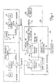
- FIGURE 1 a single node of the MPP system has a pair of PEs indicated by reference numbers 1 and 11.
- PE 1 connects over a data path to a DTB ANNEX 2.
- DTB ANNEX 2 connects to a comparison element 3, which also receives identification data WHOAMI.
- Comparison element 3 connects to a LOCAL reference data path 4 to Local DRAM Memory indicated by reference number 5, and to REMOTE reference data path 6. The functions and operation of these elements will be explained below in this specification.
- PE 11 connects to DTB ANNEX 12, which connects to comparison element 13, which also receives its own identification data WHOAMI. Comparison element 13 connects to a LOCAL reference data path 14 to Local DRAM Memory indicated by reference number 15, and to REMOTE reference data path 16.
- a network interface 48 comprises REQUEST QUEUEs 7 and 17, VIRTUAL-TO-LOGICAL converter 30, ARBITRATION element 20, and PACKET CREATION element 34.
- REMOTE reference data paths 6 and 16 connect to REQUEST QUEUEs 7 and 17, respectively, outputs of which connect over data paths 21 and 22 respectively for VIRTUAL-TO-LOGICAL converter 30.
- the output of this element connects over path 31 to LOOKUP TABLE 32.
- the output of LOOKUP TABLE 32 connects to element 34, PACKET CREATION.
- This element in turn connects to the interconnect network 50 of the MPP system. In practice, a great number of nodes such as is shown in FIGURE 1 are all connected to Network 50.
- the preferred MPP system has a physically distributed memory, wherein each processor 1, 11 has a favored, low latency, high bandwidth path to a local memory 5, 15 and a longer latency lower bandwidth access to the memory banks associated with other processors over the interconnect network 50.
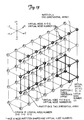
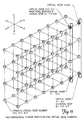
- the interconnect network is comprised of a 3-dimensional torus which when connected creates a 3-dimensional matrix of PEs. A portion of the network is shown in FIGURE 2, wherein the dots represent nodes, and the lines between dots represent interconnections in the plus and minus x, y, and z directions.
- the torus design has several advantages, including speed of information transfers and the ability to avoid bad communication links.
- the interconnect network is also scalable in all three dimensions.
- MPP system MPP system
- MPP system has a physically distributed, logically shared memory
- the address generated by the microprocessor in a PE cannot be used to directly reference physical memory. This section describes the components and the process used to reference system data and registers in the MPP system.
- the PEs within the MPP system can be identified using a virtual PE number, a logical PE number, and a physical PE number.
- the MPP system interprets the virtual PE as a PE within a user partition.
- a logical PE is a PE that is configured into the system (this excludes disabled spare node, I/O nodes, and faulty nodes).
- a physical PE is any PE within the system.
- Addresses used in the MPP system can also be identified as virtual, logical, and physical. Each type of address contains information that the MPP system uses to address local memory, reference memory-mapped registers, and route packets through the network.
- a PE is identified by one of three types of numbers: a physical PE number, a logical PE number, or a virtual PE number. All three types of numbers consists of a PE bit and a field containing the node number or node coordinates.
- Every PE in the MPP system is assigned a unique number that indicates where the PE is physically located in a system. This number is the physical PE number.
- the support circuitry in each PE contains a register called the physical PE register.
- the physical PE register When a circuit board is placed in the system cabinet, hardware automatically sets the bits of the physical PE register to indicate where the PE is located in the cabinet.
- the physical PE number contains two parts: the physical node number and the PE bit.
- the physical node number indicates which physical node the PE is located in (PE node, spare PE node, input node, or output node).
- the PE bit indicates PE 0 or PE 1 in a node.
- Table 1 shows a simplified physical PE number. More information on the exact bit format and use of the physical PE number is provided in "Register Mapping" below.
- a 512-PE MPP system may contain 520 physical PEs (not including PEs in the I/O gateways). Of these 520 PEs, 512 PEs are used in the logical system and 8 PEs (in 4 spare PE nodes) are used as spare PEs.
- Each physical PE used in a logical system is assigned a unique logical PE number.
- the logical PE number identifies the location of a PE in the logical system of nodes.
- the logical PE number contains two parts: the logical node number and the PE bit.
- the logical node number indicates which logical node the PE resides in (processing element node, input node, or output node).
- the PE bit indicates whether the PE is PE 0 or PE 1.
- Table 2 shows a simplified format of the logical PE number. More information on the exact bit format of the logical PE number is provided in "Register Mapping" below.
- the logical nodes form a three-dimensional matrix of nodes.
- Figure 2 shows the logical PE nodes for a 128-PE MPP system. Although the system actually contains 68 physical PE nodes, only 64 of the nodes are used in the logical system. The remaining 4 spare physical nodes are physically connected to the interconnect network but are not given logical node numbers.
- This type of configuration enables a spare node to logically replace a failing node. When this occurs, the spare node obtains a logical number and the failing node does not receive a new logical node number.
- the support software running on the host system determines the resources needed for the application and creates a partition for the application to run in.
- a partition is a group of PEs and a portion of the barrier synchronization resources that are assigned to one application.
- the application uses virtual PE numbers to reference the PEs in a partition.
- an operating system partition when the application transfers data between PEs, the operating system must be involved with the transfer. (When multiple references to the same PE are made, the operating system is involved with the first transfer to the remote PE. Subsequent transfers to the same PE do not involve the operating system.)
- the operating system converts the virtual PE numbers used by the application into logical PE numbers.
- Hardware in each PE node converts the virtual PE numbers used by the application into logical PE numbers.
- the virtual PE number contains two parts: The virtual node number and the PE bit.
- the virtual node number ranges from 1 to 10 bits and indicates which processing element node in a hardware partition the PE resides in.
- the PE bit indicates when the PE is PE0 or PE1 in the node (refer to Table 3).
- the virtual node number has 0 to 3 bits assigned to the X dimension, 0 to 4 bits assigned the Y dimension, and 0 to 3 bits assigned to the Z dimension.
- software arranges the virtual nodes into one of several shapes. For example, a three-bit virtual node number indicates there are eight nodes in the hardware partition. These nodes may be arranged in 1 of 10 shapes.
- Table 4 lists the possible node shapes for a three-bit virtual node number. For each shape, the number of nodes in each dimension is limited to powers of two (1, 2, 4, 8, 16, etc.).
- Figure 3 shows three of the eight-node partition shapes in a 128-PE MPP system.
- Figure 4 shows a two-dimensional, eight-node partition that contains 16 PEs. Each node in the partition is referred to by the three-bit virtual node numbers shown in Figure 3.
- This two-dimensional array of eight nodes may actually correspond to one of many eight-node two-dimensional arrays in the logical system.
- Figure 5 shows two examples of how this two-dimensional array may be placed in the logical system of nodes in a 128-PE MPP system.
- a virtual node number does not always correspond to the same logical node number.
- the virtual address is a byte oriented address generated by a program compiler.
- the virtual address may contain three parts: a segment, a virtual index, and a virtual address offset.
- Table 5 shows the bit format of the virtual address. Although the length is 64 bits, only 41 bits of the address are actually used.
- the microprocessor operating system software specifies how the microprocessor hardware maps the virtual address into the partial physical address. Because this process if defined by software, the format of the virtual address may be changeable, but the format shown in Table 5 is included as an example of how the microprocessor interprets a virtual address.
- the segment is a four-bit number that divides the virtual address space into up to 16 segments.
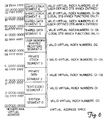
- Each segment identifies a unique type of memory. For example, when the segment number is set to 4, information may be written to or read from memory-mapped registers in the support circuitry of a PE or in other components of a PE node (refer to Figure 6).
- a private segment refers to information that is stored in the local memory of a PE and is used only by the microprocessor in the PE. Only the microprocessor in the PE can write to or read from a segment designated as private.
- a shared segment refers to information that may be stored in any PE in the system and may be used by any microprocessor in a partition.
- the shared segments are located in the same area of local memory in all of the PEs within a partition.
- the virtual index is a 5-bit number that references one of the entries in the DTB annex.
- the DTB annex is a 32-entry table external to the microprocessor (in the support circuitry of a PE, references 2, 12 in Figure 1) that contains information used to expand the addressing range of the microprocessor to include all of system memory.
- Each entry in the DTB annex contains two parts: a PE number and a memory function code (FC).
- FC memory function code
- the PE number contains a node number and PE bit.
- the node number can be a virtual node number or a logical node number.
- the PE bit indicates the PE in which the memory function will occur.
- the function code is a 3-bit number that indicates the memory reference function that the PE will perform.
- Table 7 lists the function codes and the corresponding memory functions.
- Each entry in the DTB annex describes a memory reference function that the PE will perform. Entry 0 of the DTB annex is reserved for use by the operating system and will always contain a logical PE number. Two bits of the system control register determine whether the remaining 31 entries contain virtual or logical PE numbers.
- the system control register is a memory-mapped register located in the support circuitry of a PE.
- SCR system control register
- bit 0 of the system control register enables entries 0 through 15 of the DTB annex so they may be written to by the user or the operating system (entries 1 through 15 are then interpreted as virtual PE numbers).
- bit 0 of the system control register disables the ability to write to entries 0 through 15 of the DTB annex (entries 0 through 15 are then interpreted as logical PE numbers).
- bit 1 of the system control register when set to 1, enables entries 16 through 31 of the DTB annex so they may be written to by the user or operating system (entries 16 through 31 are then interpreted as virtual PE numbers). When set to 0, bit 1 of the system control register disables the ability to write to entries 16 through 31 of the DTB annex (entries 16 through 31 are then interpreted as logical PE numbers).
- Table 8 shows the entries for a sample DTB annex.
- bit 1 of the system control register is set to 1 and bit 0 is set to 0.
- Entry 0 is reserved for use by the operating system.
- the virtual address offset is a byte oriented address that points to a byte within a segment of the virtual address space.
- the lower 32 bits of the virtual address define the offset.
- the virtual address offset may range from zero to four giga-bytes.
- the microprocessor After receiving the virtual address from an application program, hardware in the microprocessor converts the virtual address into a partial physical address.
- the partial physical address is an address that the microprocessor place on the address pins of the microprocessor.
- the address pins of the microprocessor do not directly address a physical memory. Instead, support circuitry in the PE interprets the partial physical address and routes data between the microprocessor and either local memory, memory-mapped registers, or memory in a remote PE.
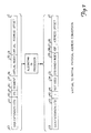
- Figure 7 shows how a microprocessor maps a virtual address into a partial physical address.
- the partial physical address contains three parts: the DTB annex index, the address space partition (ASP), and the address offset. Bits 34 through 63 of the partial physical address are not placed on output pins of the microprocessor and are not used.
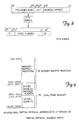
- the DTB annex index is a 5-bit number that references one of the 32 entries in the physical DTB annex (refer to Figure 8).
- the DTB annex After receiving the DTB annex index from the microprocessor, the DTB annex sends the contents of the appropriate DTB annex entry to the PE support circuitry. The support circuitry then interprets the DTB annex information to determine what type of memory function to perform and where to perform the memory function.
- the support circuitry interprets the entries of the DTB annex as virtual PE numbers and function codes.
- the support circuitry interprets the entries of the DTB annex as logical PE numbers and function codes.
- the support circuitry always interprets entry 0 of the DTB annex as a logical PE number and a function code that is defined by the operating system.
- the address space partition bits divide the address space for bits 0 through 28 of the partial physical address into three regions (refer to Table 9).
- Bit 28 divides the partial physical address space into local memory and memory-mapped register space.
- Bit 27 further divides the local memory space into local memory with SECDED protection and local memory without SECDED protection.
- Figure 9 shows a map of the partial physical address space for a PE.
- the address space for local memory with SECDED protection provides up to 128 Mbytes (16 Mwords) of memory; however, not all of the address space is used. For example, MPP systems with local memory sizes of 2 Mwords (16 Mbytes) per PE use only the 23 least significant bits of the address offset. The 16 Mwords of address space is provided for future expansion of system memory.
- the address space for local memory without SECDED protection provides up to 16 Mwords of memory; however, not all of this address space is used.
- the information stored in this section of local memory address space is from the headers of messages.
- the address space for memory-mapped registers contains the addresses for information that is stored or read from memory-mapped registers.
- Memory mapped-registers are registers that are located in the support circuitry of a PE or other components of a PE node but are addressed by the local microprocessor as if they were located in a local memory.
- the microprocessor when the microprocessor stores information in a register that controls the block transfer engine, the microprocessor performs a write operation to the address that points to the block transfer engine register. After receiving the data and address information, the support circuitry in the PE routes the data to the appropriate register instead of storing the information in local DRAM memory.
- the address offset is a byte oriented address that points to a byte in the local memory of a PE; however, the support circuitry in the PE may not use the last 2 bits of the address offset portion of the partial physical address.
- the support circuitry interprets bits 3 through 26 of the address offset as a word oriented address that points to a 64-bit word in the local memory of a PE. Because the support circuitry may only use bits 3 through 26 of the address offset, the term "address offset" also refers to a 24-bit address offset that references a 64-bit word in local memory.
- the microprocessor and DTB annex present the support circuitry with address information.
- the support circuitry may interpret this information as an address for a virtual PE or as an address for a logical PE.
- the support circuitry interprets the address information as a virtual PE address.
- the support circuitry receives four types of information from the microprocessor and DTB annex: a memory function code, a virtual PE number, the ASP bits, and an address offset (refer to Figure 10).
- the support circuitry After receiving the virtual PE number from the DTB annex, the support circuitry compares the value of the virtual PE number to the value stored in a virtual PE (V_WHOAMI) register.
- V_WHOAMI virtual PE
- the V_WHOAMI register contains the virtual PE number of the PE and is loaded by the operating system when the partitioning of the MPP system changes.
- the microprocessor When the virtual PE number from the DTB annex matches the PE number stored in the V_WHOAMI register, the microprocessor is requesting that a memory function be performed in the local PE. After interpreting the function code bits that select which memory function to perform, the support circuitry transfers information between the microprocessor and local memory or between the microprocessor and a memory-mapped register (the location is specified by the ASP bits).
- the microprocessor When the virtual PE number from the DTB annex does not match the PE number stored in the V_WHOAMI register, the microprocessor is requesting that a memory function be performed in a remote PE. When the microprocessor requests that a memory function be performed in a remote PE, the support circuitry checks the value of the virtual PE number to ensure that it is less than the highest numbered virtual PE in the hardware partition.
- the support circuitry checks the value of the virtual PE number it received from the DTB annex by comparing the PE number to the virtual PE range mask stored in the virtual PE range mask (VRT_RG) register.
- VRT_RG virtual PE range mask
- This register is loaded by the operating system when the partitioning of the MPP system changes. Bit 0 of the VRT_RG register is not used. Bits 1 through 10 of the VRT_RG register contain a contiguous field of 0's in the legal bit positions for the size of the user partition and the remaining bits are set to 1's (refer to Table 10).
- the support circuitry in the PE After checking the value of the virtual PE number, the support circuitry in the PE sends address and control information to the network interface.
- the network interface uses this information to create packets.
- the support circuitry interprets the address information as a logical PE address.
- the support circuitry receives four types of information from the microprocessor and DTB annex: a memory function code, a logical PE number, the ASP bits, and an address offset (refer to Figure 11).
- the support circuitry After receiving the logical PE number from the DTB annex, the support circuitry compares the value of the logical PE number to the value stored in a logical PE (L_WHOAMI) register.
- L_WHOAMI register contains the logical PE number of the PE and is loaded by the operating system when the MPP system is initialized.
- the microprocessor When the logical PE number from the DTB annex matches the PE number stored in the L_WHOAMI register, the microprocessor is requesting that a memory function be performed in the local PE. After interpreting the function code bites that select which memory function to perform, the support circuitry transfers information between the microprocessor and local memory or between the microprocessor and a memory-mapped register (the location is specified by the ASP bits).
- the microprocessor When the logical PE number from the DTB annex does not match the PE number stored in the L_WHOAMI register, the microprocessor is requesting that a memory function be performed in a remote PE. When this occurs, the support circuitry in the PE does not perform a range check on the logical PE number. The support circuitry sends address and control information directly to the network interface for use in a packet.
- the network interface receives address information and data from PE 0, PE 1, or the block transfer engine in a processing element node (refer to Figure 12).
- the address information may be virtual PE address information or logical PE address information.
- the network interface must convert the virtual PE information into logical PE information before using the information to create a packet.
- the virtual PE number may correspond to different logical PE numbers. Because of this characteristic, the network interface cannot directly use a virtual PE number to determine to which logical PE a memory function will be directed. The network interface must convert the virtual PE number into a corresponding logical PE number.
- Figure 13 shows three 8-node partitions (partitions A, B, and C) in a 128-PE MPP system.
- a virtual PE number refers to a PE in the partition.
- the virtual PE number contains a virtual node number and PE bit.
- the virtual node number in all three partitions is a 3-bit number.
- All 3 bits of the virtual node number for partition A are assigned to the X dimension (refer again to Figure 13).
- partition B bits 0 and 1 of the virtual node number are assigned to the X dimension and bit 2 is assigned to the Y dimension.
- partition C bit 0 of the virtual node number is assigned to the X dimension, bit 1 is assigned to the Y dimension, and bit 2 is assigned to the Z dimension.
- the network interface uses a three-step process to convert the virtual PE number into a logical PE number.
- the network interface reformats the virtual node number (which may be a 1- to 10-bit number) into a 10-bit virtual node number (refer to Figure 14).
- the network interface compares the 3 least significant bits of the reformatted virtual node number to the X mask.
- the X mask is a contiguous, right-justified field of 1's that indicates how many bits of the virtual node number are assigned to the X dimension. When a bit in the X mask is set to 1, the corresponding bit of the virtual node number is valid. When a bit in the X mask is set to 0, the corresponding bit of the virtual node number is not used for the X dimension.
- the network interface then shifts the reformatted virtual node number 0 to 3 bits to the right until the first bit that is assigned to the Y dimension is in the 0 bit location.
- the network interface compares the 4 least significant bits of the shifted virtual node number to the Y mask. When a bit in the Y mask is set to 1, the corresponding bit of the shifted virtual node number is valid. When a bit in the Y mask is set to 0, the corresponding bit of the shifted virtual node number is not used for the Y dimension.
- the network interface then shifts the original reformatted virtual node number 0 to 7 bits to the right until the first bit that is assigned to the Z dimension is in the 0 bit location.
- the network interface compares the 3 least significant bits of the shifted virtual node number to the Z mask. When a bit in the Z mask is set to 1, the corresponding bit of the shifted virtual node number is valid. When a bit in the Z mask is set to 0, the corresponding bit of the shifted virtual node number is not used for the Z dimension.
- the network interface After reformatting the virtual node number into a 10-bit virtual node number, the network interface adds a base node address to the 10-bit virtual node number (refer to Figure 15).
- the base node address is the logical node number of the smallest numbered virtual PE node in a partition.
- Table 12 lists the base node addresses for the three partitions shown in Figure 13.
- Table 12 also lists the shift and mask values for each partition.
- the network interface After adding the base node address to the 10-bit virtual node number, the network interface compares the two most significant bits of the X, Y, and Z-dimension numbers to the X-, Y-, and Z-dimension configuration masks (refer to Figure 16). When a bit of the X-, Y-,or Z-dimension configuration mask is set to 0, the corresponding bit in the X-, Y-, or Z-dimension number is valid. When a bit of the X-, Y-, or Z-dimension is set to 1, the corresponding bit in the X-, Y-, or Z-dimension number is set to 0.
- Figure 17 shows a two-dimensional, four-node partition in a 128-PE MPP system.
- the network interface first reformats the virtual node number into a 10-bit virtual node number.
- the network interface After reformatting the virtual node number into a 10-bit virtual node number, the network interface adds the base node address to the virtual node number (refer to Table 11).
- the Y-dimension portion of the temporary logical node number is four. This value is larger than the largest numbered node in the Y dimension (refer again to Figure 17).
- the base, shift, mask, and configuration mask values for all three dimensions are stored in a register called the network interface PE adjust (LPE_XLATE) register. This register is loaded by the operating system when the partitioning of the MPP system changes.
- the operating system defines the partitions in the logical MPP system. More information on the LPE_XLATE register is provided in "Register Mapping" in this section.
- the network interface receives a logical PE number in one of two ways: directly from a PE or the BLT in the processing element node, or by converting a virtual PE number into a logical PE number. As was previously described. the logical PE number may not always correspond to the same physical PE in the MPP system.
- the logical PE number contains two parts: the logical node number and the PE bit. Because the logical node number does not always correspond to the same physical node, the network interface cannot use the logical node number to calculate how to route information to the correct physical node.
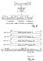
- the network interface in each node uses a look-up table to obtain the routing tag. Circuitry in the network interface enters the logical node number into the routing tag look-up table. The routing tag look-up table then provides the routing tag that corresponds to that logical node (refer to Figure 18).
- the routing tag contains information that indicates the path a packet must follow through the interconnect network to get from the physical source node to the physical destination node. This information includes how many hops to complete in each dimension, what direction to travel in each dimension, and which virtual channel (VC) to use in each dimension.
- VC virtual channel
- the routing tags for each node in the MPP system are generated by a program that runs in the host system.
- the routing tag calculation program uses a configuration file that contains information on each node and communication link in the MPP system.
- the system administrator modifies the configuration file in the host system.
- the administrator then runs the routing tag calculation program.
- the program generates new routing tags that steer information around a bad node or communication link.
- routing tags are written into the routing tag look-up table of each node in the system. More information of the addresses and format of the routing tag look-up table is provided in "Register Mapping" in this section.
- the network interface generates information and uses the information it receives from a PE or the BLT to create packets.
- Table 13 lists the types of packets the network interface creates during various functions.
- Figure 19 shows the format of each packet type. Each packet contains a header and may contain data. The following subsections describe each phit of the header and data portions of a packet.
- Every packet contains a header.
- the header may consist of the following types of phits: a routing tag phit, a destination phit, a command phit, request address phits, a source phit, or response address phits. The following paragraphs describe each type of phit.
- Every packet contains a routing tag phit.
- the X-dimension switch in the network router examines bits 0 through 3 of the routing tag. When bits 0 through 3 are equal to zero, the X-dimension switch sends the routing tag information to the Y-dimension switch in the network interface. As the X-dimension switch sends information to the Y-dimension switch, the bits of the routing tag are rearranged on the circuit board so that bits 0 through 3 contain the ⁇ Y bits.
- the bit format of the routing tag phit is rearranged on the circuit board each time information transfers between the X- and Y-dimension switches or between the Y- and Z-dimension switches in the network interface.
- the bits of the routing tag phit are rearranged so the same gate array types can be used for the X-, Y-, and Z-dimensions.
- the X-dimension switch checks the value of the ⁇ X bit. This bit indicates when the packet should be sent on the +X or -X communication link. The X-dimension switch then checks the value of the X VC bit to determine which virtual channel to use on the communication link. (For more information about refer "Routing Tag Look-up Table Low-order Bits Registers" later in this section.) After checking the value of these two bits, the X-dimension switch increments the value of the ⁇ X portion of the routing tag phit by one and sends the phit to the network interface of the next node in the +X or -X direction. (The ⁇ X portion is incremented because it contains the two's compliment of the number of hops to complete in the X dimension.)
- Every packet contains a destination phit.
- the destination phit contains the destination PE number (refer to Table 15).
- the destination PE number is the logical PE number of the PE that will receive the packet.
- the network interface obtains the destination PE number from bits 0 through 11 of the destination logical PE number that was read from the DTB annex or that was converted from the virtual PE number read from the DTB annex.
- Every packet also contains a command phit with information that indicates to the destination PE what type of function to perform.
- the network interface formats the command information after it receives the information from the support circuitry in a PE or BLT.
- Bits 0 through 11 of the command phit contain a command field (refer to Table 16).
- Bit 12 indicates when the packet will go to PE 0 or PE 1 in the destination PE node.
- Bits 13 and 14 of the command phit contain an even parity bit for bits 8 through 12 and 0 through 7, respectively. When set to 1, bit 15 indicates the packet is an error message created by the network interface from an incorrectly routed packet.
- the command field contains three parts: a packet type field, a request or response bit, and a command (refer to Table 17).
- the packet type field indicates what type of packet the command phit is in (refer again to Figure 19). When set to 1, the request or response bit indicates the packet is a request packet. When set to 0, the request or response bit indicates the packet is a response packet.
- the command indicates what function to perform.
- All the phits in a packet, except the routing tag, destination, and data phits are protected by parity bits.
- the network interface receives each phit of a packet (except the routing tag, destination, and data phits), the network interface generates 2 new parity bits.
- the network interface sets bit 1 of the system status register (SSR) to 1, converts the packet into an error message, and sends the error message to PE 0 or PE 1 (identified in the command phit).
- SSR system status register
- the request address points to one 64-bit word or the first word in a 4-word block of data in the memory of a PE.
- the network interface obtains the request address from the address offset generated by a PE or the BLT.
- Table 18 shows the format of the request address phits.
- the BLT error bit (bit 12) is used to indicate one of three BLT errors in request packet types 4 or 6.
- bit 12 When the BLT issues a write request (packet type 4 or 6) and the BLT error bit is set to 1, the BLT aborts the transfer.
- Every request packet also contains a source phit.
- the source phit contains the source node number, which is the logical node number of the node creating the request packet.
- the source phit also contains a PE bit that indicates which PE in the source node created the packet.
- Table 19 shows the format of the source phit.
- the node that receives the request packet uses the source node number as the destination node number in a response packet.
- the network interface generates the source node number by reading the node number stored in a register called the network interface source (X_WHOAMI) register.
- the network interface also uses the X_WHOAMI register to check if a packet was routed to the correct node. After receiving a packet, the network interface compares the node number stored in the X_WHOAMI register with the destination node number in the packet. When the numbers are equal, the packet arrived at the correct destination node. When the numbers are not equal, an error occurred and the packet arrived at the wrong node.
- the network interface then converts the packet into an error message and sends the message to PE 0 or PE 1 in the node that received the packet (according to the PE bit that is stored in the command field of the packet).
- the microprocessor can then examine the message to try and determine the cause of the error.
- a request or response packet may also contain a response address.
- the response address points to a location in local memory of the source PE where 1 word or 4 words of data from a read response packet will be stored.
- Table 20 shows the format of the response address phits.
- the BLT error bit (bit 12) is used to indicate a BLT range error in request packet type 2 or response packet type 4 or 6.
- packet type 2 When the BLT issues a read request (packet type 2) and the BLT error bit is set to 1 in response address phit 0, the PE that receives the packet performs the memory read and creates a response packet type 4 or 6. The PE also sets the BLT error bit to 1 in response address phit 0 of the response packet. The PE that receives the response packet then does not perform the memory write.
- Both request and response packets may contain data.
- Data is one 64-bit word or four 64-bit words that will be used by the PE receiving the packet.
- the network interface receives data for a packet from a PE in the processing element node. Seven check bits (used by the microprocessor to check the data for errors) are sent along with each 32-bit halfword.
- Figure 20 shows the format of the data phits for word 0 in a packet.
- the MPP system uses several memory-mapped registers when interpreting addressing information. These registers are used to identify where a PE is located, check the value of virtual and logical PE numbers, and create the routing tag.
- registers used for addressing in the MPP system.
- registers memory-mapped registers
- Table 21 is a summary of the registers and their names. Table 38 provides additional information related to the address memory-mapped registers. Table 21 also lists the partial physical address of each register as they appear on the address pins of the microprocessor.
- the shared registers include the X_WHOAMI, LPE_XLATE, ROUTE_LO, ROUTE_HI, NET_ENA, NET_PFM, NOED_CSR, and BLT registers.
- the addresses for each of the registers are given according to the partial physical address as they appear on the pins of the microprocessor.
- the physical PE number register (P_WHOAMI) is a 12-bit, read-only, system privileged register that contains the physical PE number.
- the physical PE number is a unique number assigned to each PE in the system and indicates where the PE is physically located in a system cabinet.
- Table 22 shows the bit assignments for the P_WHOAMI register address as they appear on the address pins of the microprocessor.
- the operating system uses the values stored in the P_WHOAMI registers to load the logical PE number registers of the MPP system when the system is deadstarted. This provides a unique temporary logical PE number for each physical PE in the system and allows the operating system to transfer deadstart information to all the PEs in the system. After the system is deadstarted, the logical PE number registers are loaded with the appropriate logical PE numbers.
- PEMs processing element modules
- IOMs input/output modules
- Table 23 shows the bit format of the P_WHOAMI register, and the following subsections describe each bit of the register.
- the PE number bit indicates whether the PE is PE 0 or PE 1 in a processing element node. When set to 1, the PE is PE 1; and when set to 0, the PE is PE 0. When the PE is in an input node or an output node, this bit is set to 0.
- the X-dimension number ranges from 0 through 7.
- the node number bit indicates which node on a printed circuit board the PE resides in. On a processing element printed circuit board, this bit indicates whether the PE resides in processing element node 0 or processing element node 1. On an I/O gateway printed circuit board, this bit indicates whether the PE resides in the input node (node 0) or output node (node 1).
- This bit indicates which printed circuit board on a PEM or an IOM the PE resides.
- the printed circuit boards are also referred to as board A(0) and board B(1).
- the chassis ID bits indicate which cabinet in a multiple cabinet configuration the PEM or IOM resides.
- the Z coordinate bits are set to different values depending on which type of module the PE resides. These modules are the standard PEM, the spare PEM, and the IOM.
- these bits indicate the Z-dimension portion of the physical node number.
- the Z-dimension number ranges from 0 through 7.
- the Z-coordinate bits are set to one (001).
- the I/O or spare PE bit is also set to 1. This sets the total Z-dimension and I/O or spare PE bit portion of the physical PE number to nine (1001).
- this bit indicates that the PE resides on a spare PEM or an IOM.
- the Z-coordinate bits are set to one (001).
- the Z-coordinate bits are set to four (100).
- the logical PE number register (L_WHOAMI) is a 12-bit, write-only, system privileged register that contains the logical PE number.
- the logical PE number is a unique number that is assigned by the operating system to each physical PE used in the logical MPP system.
- the support circuitry uses the L_WHOAMI register to check whether a memory function is to be performed in the local PE or a remote PE.
- Table 24 shows the bit assignments for the L_WHOAMI register address as they appear on the address pins of the microprocessor.
- Table 25 shows the bit format of the L_WHOAMI register and describes each bit in the register.
- V_WHOAMI The virtual PE number register
- the virtual PE number register is an 11-bit, write-only, system privileged register that contains the virtual PE number.
- the virtual PE number is a number assigned by the operating system to a logical PE in a partition.
- the support circuitry uses the V_WHOAMI register to check whether a memory function is to be performed in the local PE or a remote PE.
- Table 26 shows the bit assignments for the V_WHOAMI register address as they appear on the address pins of the microprocessor.
- Table 27 shows the bit format of the V-WHOAMI register and describes each bit in the register.
- the virtual PE range mask register (VRT_RG) is a 10-bit, write-only, system privileged register that contains the virtual PE range mask.
- the virtual PE range mask contains a contiguous field of 0's in the legal bit positions for the size of the user partition. The remaining bits are set to 1's.
- Table 28 shows the bit assignments for the VRT_RG register address as they appear on the address pins of the microprocessor.
- Table 29 shows the bit format of the VRT-RG register and describes each bit. For examples of virtual range masks, refer again to Table 10.
- the network interface source register (X_WHOAMI) is an 11-bit, write-only, system privileged register that contains the source logical node number.
- the network interface uses the source logical node number to indicate which logical node created a packet (source phit).
- Table 30 shows the bit assignments for the X_WHOAMI register address as they appear on the address pins of the microprocessor.
- Table 31 shows the bit format of the X-WHOAMI register and describes each bit register.
- the network interface also uses the X_WHOAMI register to check the value of the destination logical node number in a packet header. After receiving a packet, the network interface compares the node number stored in the X_WHOAMI register with the destination node number in the packet. When the numbers are equal, the packet arrived at the correct destination node. When the numbers are not equal, a network packet error occurred and the packet arrived at the wrong node.
- the network interface PE adjust register (LPE_XLATE) is a 31-bce PE adjust register contains the shift, base, mask, and configuration mask values used to translate a virtual node number into a logical node number (refer again to Figures 13-16).
- Table 32 shows the bit assignments for the LPE_XLATE register address as they appear on the address pins of the microprocessor.
- Table 41 shows the bit format of the LPE_XLATE register and describes each bit of the register.
- Table 39 lists the values of the configuration masks for each configuration of the MPP system.
- the routing tag look-up table low-order bits registers are 12-bit, write-only, system privileged registers that each contain the 12 low-order bits of a routing tag.
- Table 40 shows the bit assignments for a ROUTE_LO register address as they appear on the address pins of the microprocessor.
- Bits 5 through 15 of the address indicate one of the 2,048 ROUTE_LO registers.
- Each ROUTE_LO register corresponds to one destination logical node number.
- Table 33 shows the bit format of each ROUTE_LO register and describes each bit in the register.
- Figure 21 shows eight nodes in the X dimension of a MPP system. For clarity, the communication links that connect to the other nodes in the Z and Y dimensions are not shown. This figure is used as a reference for the following examples.
- the ⁇ X value is set to E 16 because E is the two's compliment of 2.
- the ⁇ X value is set to 0 because the packet will travel in the positive X direction.
- the X VC select bit 0 is set to 0 because the packet does not cross the dateline in the X dimension when it travels through the network.
- the ⁇ X value is set to D because D is the two's compliment of 3.
- X 7.
- the ⁇ X value is set to 1 because the packet will travel in the negative X direction.
- the X VC select bit 0 is set to 1 because the packet does cross the dateline in the X dimension when it travels through the network.
- the eight nodes shown in Figure 21 do not connect to an I/O gateway, a spare processing element node, or both an I/O gateway and a spare processing element node, the routing tags must contain values that reflect the number of hops a packet makes when traveling through that dimension.
- Figure 22 shows eight processing element nodes, an I/O gateway, and a spare processing element node in the X-dimension of a MPP system. For clarity, the communication links that connect to the other nodes in the Z- and Y-dimensions are not shown.
- the ⁇ X value is set to 1 because the packet will travel in the negative X direction.
- the X VC select bit 0 is set to 0 because the packet does not cross the datelines in the X dimension when it travels through the network.
- the ⁇ X value is set to 0 because the packet will travel in the positive X direction.
- the X VC select bit is set to 0 because the packet does not cross the dateline in the X-dimension when it travels through the network.
- the routing tag look-up table high-order bits registers are 6-bit, write-only, system privileged registers that each contain the 6 high-order bits of a routing tag.
- Table 34 shows the bit assignments for a ROUTE_HI register address as they appear on the Address pins of the microprocessor.
- Bits 5 through 15 of the address indicate one of the 2,048 ROUTE_HI registers.
- Tables 35 and 36 shows the bit format of each ROUTE_HI register and describes each bit of the register.
- Eight-node Partition Shapes Eight-node Array Shaped in X, Y, Z Description 8,1,1 One-dimensional array in the X dimension 1,8,1 One-dimensional array in the Y dimension 1,1,8 One-dimensional array in the Z dimension 1,2,4 Two-dimensional array in the Y-Z plane 1,4,2 Two-dimensional array in the Y-Z plane 2,1,4 Two-dimensional array in the X-Z plane 4,1,2 Two-dimensional array in the X-Z plane 2,4,1 Two-dimensional array in the X-Y plane 4,2,1 Two-dimensional array in the X-Y plane 2,2,2 Three-dimensional array Memory Function Codes Function Code Bits 14 - 12 Memory Function 000 Write or noncacheable read 001 Write or nonchacheable atomic swap 010 Fetch-and-increment write or read 011 Reserved (may cause an error interrupt) 100 Write or cached read 101 Write or cached atomic swap 110 Write or cached read ahead 111 Message or cached read Configuration Mask Example Z Y X 000 0001 001 10-
Landscapes
- Engineering & Computer Science (AREA)
- Theoretical Computer Science (AREA)
- Physics & Mathematics (AREA)
- General Engineering & Computer Science (AREA)
- General Physics & Mathematics (AREA)
- Multi Processors (AREA)
Claims (14)
- Un système de traduction d'adresse dans un système informatique à processeurs multiples comprenant une pluralité de noeuds de traitement interconnectés par un réseau d'interconnexion à n dimensions (50), chaque noeud de traitement comprenant un élément de traitement comportant un processeur (1, 11) et une mémoire locale (5, 15), dans lequel les parties adressables globalement de la mémoire locale (5, 15) de chaque élément de traitement forment une mémoire répartie, le système de traduction d'adresse étant caractérisé par :le fait que chaque élément de traitement est identifié par un numéro physique correspondant à un emplacement physique de l'élément de traitement dans le système informatique à processeurs multiples ;le fait que chaque élément de traitement dans une configuration logique d'éléments de traitement est identifié par un numéro logique correspondant à un emplacement logique de l'élément de traitement dans la configuration logique ;le fait que chaque élément de traitement dans une partition d'utilisateur d'éléments de traitement pour exécuter une application est identifié par un numéro virtuel correspondant à un emplacement virtuel de l'élément de traitement dans la partition d'utilisateur ; etune interface de réseau (48) dans chaque noeud de traitement pour générer des paquets d'informations devant être fournis à un noeud de destination sur la base des informations basées sur un numéro virtuel ou logique provenant du noeud de traitement respectif, dans lequel chaque paquet contient une étiquette d'acheminement comportant des informations basées sur un numéro physique indiquant un chemin du noeud de traitement respectif au noeud de destination.
- Le système de traduction d'adresse selon la revendication 1 comprenant, de plus :
une table de correspondance (32) dans chaque noeud de traitement pour mémoriser les étiquettes d'acheminement, dans lequel l'interface de réseau correspondante fournit un numéro logique correspondant aux éléments de traitement du noeud de destination pour indexer l'étiquette d'acheminement correspondant audit numéro logique. - Le système de traduction d'adresse selon la revendication 2, dans lequel l'interface de réseau comprend du matériel (30) pour traduire des informations basées sur un numéro virtuel en un numéro logique pour indexer la table de correspondance.
- Le système de traduction d'adresse selon la revendication 1 ou 2, dans lequel chaque élément de traitement comprend du matériel pour traduire des informations basées sur un numéro virtuel en informations basées sur un numéro logique.
- Le système de traduction d'adresse selon l'une quelconque des revendications précédentes, dans lequel le réseau d'interconnexion (50) comprend des canaux virtuels pour acheminer des paquets entre des noeuds et dans lequel les informations basées sur un numéro physique dans l'étiquette d'acheminement comprennent des informations représentant combien de sauts dans le réseau d'interconnexion doivent être effectués dans chaque dimension, dans quelle direction le déplacement doit être effectué dans chaque dimension et quel canal virtuel, s'il y en a un, doit être utilisé dans chaque dimension pour arriver au noeud de destination.
- Le système de traduction d'adresse selon l'une quelconque des revendications précédentes comprenant, de plus :
un système hôte agencé afin d'exécuter un programme pour générer les étiquettes d'acheminement pour chaque noeud en se basant sur un fichier de configuration contenant des informations concernant chaque noeud et le réseau d'interconnexion qui relie les noeuds. - Le système de traduction d'adresse selon la revendication 6, dans lequel le fichier de configuration contient la configuration logique d'éléments de traitement qui est modifiable afin de remplacer un noeud défaillant contenant un élément de traitement dans la configuration logique par un noeud de rechange comportant un élément de traitement qui n'est pas compris dans la configuration logique en attribuant le numéro logique du noeud défaillant au noeud de rechange.
- Le système de traduction d'adresse selon l'une quelconque des revendications précédentes, dans lequel chaque noeud de traitement comprend, de plus : un moteur de transfert de bloc pour redistribuer des données entre les parties adressables globalement de la mémoire locale sans interrompre les processeurs associés.
- Le système de traduction d'adresse selon la revendication 8, dans lequel le moteur de transfert de bloc comprend du matériel pour traduire des informations basées sur un numéro virtuel en informations basées sur un numéro logique.
- Le système de traduction d'adresse selon l'une quelconque des revendications précédentes comprenant, de plus :
une table d'annexe (2, 12) dans chaque noeud de traitement contenant des informations indexées par une partie d'une adresse fournie par le processeur associé pour élargir la plage d'adressage du processeur afin d'inclure toute la mémoire répartie. - Le système de traduction d'adresse selon l'une quelconque des revendications précédentes comprenant, de plus :
une pluralité de routeurs de réseau, chaque routeur de réseau étant couplé à une interface de réseau correspondante d'un noeud de traitement et au réseau d'interconnexion, et chaque routeur de réseau comprenant n types de commutateurs de dimension correspondant à chacune des n dimensions du réseau d'interconnexion, les commutateurs de dimension étant sensibles à l'étiquette d'acheminement pour acheminer les paquets d'informations du noeud de source au noeud de destination le long du réseau d'interconnexion. - Un procédé de traduction d'adresse dans un système informatique à processeurs multiples comportant une pluralité d'éléments de traitement (PE) (1, 11) interconnectés par un réseau d'interconnexion à n dimensions (50) et comportant une mémoire répartie constituée de parties adressables globalement de la mémoire locale (5, 15) associée localement aux éléments de traitement individuels (1, 11), le procédé étant caractérisé par les étapes consistant à :définir des adresses physiques pour les éléments de traitement (1, 11) et leur mémoire locale associée (5, 15), les adresses physiques correspondant aux emplacements physiques des éléments de traitement dans le système informatique à processeurs multiples ;définir des adresses logiques pour les éléments de traitement (1, 11) et leur mémoire locale associée (5, 15) dans une configuration logique d'éléments de traitement, les adresses logiques correspondant aux emplacements logiques des éléments de traitement dans la configuration logique d'éléments de traitement ;définir des adresses virtuelles pour les éléments de traitement (1, 11) et leur mémoire locale associée (5, 15) dans une partition d'utilisateur des éléments de traitement pour exécuter une application correspondant aux emplacements virtuels des éléments de traitement dans la partition d'utilisateur ;traduire les adresses virtuelles émises par les éléments de traitement en adresses logiques ; ettraduire lesdites adresses logiques en adresses physiques pour acheminer des paquets d'informations, devant être fournis aux noeuds de destination, sur le réseau d'interconnexion (50).
- Le procédé selon la revendication 12 comprenant, de plus, l'étape consistant à remplacer un élément de traitement défaillant dans la configuration logique d'éléments de traitement par un élément de traitement de rechange qui n'est pas compris dans la configuration logique en attribuant l'emplacement logique de l'élément de traitement défaillant à l'élément de traitement de rechange.
- Un noeud de traitement destiné à être utilisé dans le système de traduction d'adresse selon l'une quelconque des revendications 1 à 11, le noeud de traitement comprenant un élément de traitement comportant un processeur (1, 11) et une mémoire locale (5, 15) comportant des parties adressables globalement destinées à être combinées avec d'autres parties adressables globalement d'autres mémoires locales d'autres noeuds de traitement pour former une mémoire répartie et dans lequel l'élément de traitement est adapté pour être identifiable par un numéro physique correspondant à un emplacement physique de l'élément de traitement, lorsqu'il est utilisé avec un système informatique à processeurs multiples, par un numéro logique correspondant à un emplacement logique de l'élément de traitement lorsqu'il est utilisé dans une configuration logique d'éléments de traitement et par un numéro virtuel correspondant à un emplacement virtuel de l'élément de traitement lorsqu'il est utilisé dans une partition d'utilisateur d'éléments de traitement pour exécuter une application, le noeud de traitement comprenant, de plus, une interface de réseau (48) qui peut être connectée à un réseau à n dimensions (50), l'interface de réseau étant adaptée pour générer des paquets d'informations devant être fournis à un noeud de destination sur la base d'informations basées sur un numéro virtuel ou logique provenant du noeud de traitement, dans lequel chaque paquet contient une étiquette d'acheminement comportant des informations basées sur un numéro physique indiquant un chemin du noeud de traitement au noeud de destination.
Applications Claiming Priority (3)
| Application Number | Priority Date | Filing Date | Title |
|---|---|---|---|
| US165814 | 1988-03-09 | ||
| US08/165,814 US5784706A (en) | 1993-12-13 | 1993-12-13 | Virtual to logical to physical address translation for distributed memory massively parallel processing systems |
| PCT/US1994/014351 WO1995016964A1 (fr) | 1993-12-13 | 1994-12-13 | Transfert d'adresses pour systemes de traitement parallele en masse |
Publications (2)
| Publication Number | Publication Date |
|---|---|
| EP0737338A1 EP0737338A1 (fr) | 1996-10-16 |
| EP0737338B1 true EP0737338B1 (fr) | 2001-02-14 |
Family
ID=22600593
Family Applications (1)
| Application Number | Title | Priority Date | Filing Date |
|---|---|---|---|
| EP95905925A Expired - Lifetime EP0737338B1 (fr) | 1993-12-13 | 1994-12-13 | Traduction d'adresses pour systemes de traitement parallele en masse |
Country Status (5)
| Country | Link |
|---|---|
| US (1) | US5784706A (fr) |
| EP (1) | EP0737338B1 (fr) |
| JP (1) | JPH09506728A (fr) |
| DE (1) | DE69426708T2 (fr) |
| WO (1) | WO1995016964A1 (fr) |
Families Citing this family (70)
| Publication number | Priority date | Publication date | Assignee | Title |
|---|---|---|---|---|
| US5940870A (en) * | 1996-05-21 | 1999-08-17 | Industrial Technology Research Institute | Address translation for shared-memory multiprocessor clustering |
| US5860146A (en) * | 1996-06-25 | 1999-01-12 | Sun Microsystems, Inc. | Auxiliary translation lookaside buffer for assisting in accessing data in remote address spaces |
| US6295584B1 (en) * | 1997-08-29 | 2001-09-25 | International Business Machines Corporation | Multiprocessor computer system with memory map translation |
| FR2785407B1 (fr) * | 1998-10-30 | 2000-12-15 | Bull Sa | Procede pour localiser des adresses physiques dans une memoire a acces non uniforme et machine pour mettre en oeuvre ce procede |
| US6256683B1 (en) | 1998-12-23 | 2001-07-03 | Bops, Inc. | Methods and apparatus for providing direct memory access control |
| US20020028656A1 (en) * | 2000-02-02 | 2002-03-07 | Yechiam Yemini | Method and apparatus for providing forwarding and replication services on a dynamically addressed network |
| US7089289B1 (en) * | 2000-07-18 | 2006-08-08 | International Business Machines Corporation | Mechanisms for efficient message passing with copy avoidance in a distributed system using advanced network devices |
| US6604185B1 (en) | 2000-07-20 | 2003-08-05 | Silicon Graphics, Inc. | Distribution of address-translation-purge requests to multiple processors |
| US7248635B1 (en) | 2000-07-20 | 2007-07-24 | Silicon Graphics, Inc. | Method and apparatus for communicating computer data from one point to another over a communications medium |
| US7333516B1 (en) | 2000-07-20 | 2008-02-19 | Silicon Graphics, Inc. | Interface for synchronous data transfer between domains clocked at different frequencies |
| US6839856B1 (en) | 2000-07-20 | 2005-01-04 | Silicon Graphics, Inc. | Method and circuit for reliable data capture in the presence of bus-master changeovers |
| US6831924B1 (en) | 2000-07-20 | 2004-12-14 | Silicon Graphics, Inc. | Variable mode bi-directional and uni-directional computer communication system |
| US6779072B1 (en) * | 2000-07-20 | 2004-08-17 | Silicon Graphics, Inc. | Method and apparatus for accessing MMR registers distributed across a large asic |
| US6681293B1 (en) | 2000-08-25 | 2004-01-20 | Silicon Graphics, Inc. | Method and cache-coherence system allowing purging of mid-level cache entries without purging lower-level cache entries |
| US6567900B1 (en) * | 2000-08-31 | 2003-05-20 | Hewlett-Packard Development Company, L.P. | Efficient address interleaving with simultaneous multiple locality options |
| US6782464B2 (en) * | 2001-07-17 | 2004-08-24 | International Business Machines Corporation | Mapping a logical address to a plurality on non-logical addresses |
| US7162608B2 (en) * | 2001-10-24 | 2007-01-09 | Cray, Inc. | Translation lookaside buffer-based memory system and method for use in a computer having a plurality of processor element |
| US20030110205A1 (en) * | 2001-12-07 | 2003-06-12 | Leith Johnson | Virtualized resources in a partitionable server |
| US6915393B2 (en) * | 2003-01-07 | 2005-07-05 | Hewlett-Packard Development Company, L.P. | Method and apparatus for physical memory partitioning |
| US7389512B2 (en) * | 2003-05-09 | 2008-06-17 | Sun Microsystems, Inc. | Interprocess communication within operating system partitions |
| US7461080B1 (en) | 2003-05-09 | 2008-12-02 | Sun Microsystems, Inc. | System logging within operating system partitions using log device nodes that are access points to a log driver |
| US7337445B1 (en) | 2003-05-09 | 2008-02-26 | Sun Microsystems, Inc. | Virtual system console for virtual application environment |
| US8892878B2 (en) * | 2003-05-09 | 2014-11-18 | Oracle America, Inc. | Fine-grained privileges in operating system partitions |
| US20040226015A1 (en) * | 2003-05-09 | 2004-11-11 | Leonard Ozgur C. | Multi-level computing resource scheduling control for operating system partitions |
| US7437556B2 (en) * | 2003-05-09 | 2008-10-14 | Sun Microsystems, Inc. | Global visibility controls for operating system partitions |
| CN1323358C (zh) * | 2004-03-05 | 2007-06-27 | 中国科学院计算技术研究所 | 一种虚拟存储模型及其方法 |
| US7685319B2 (en) * | 2004-09-28 | 2010-03-23 | Cray Canada Corporation | Low latency communication via memory windows |
| JP4982971B2 (ja) * | 2004-09-29 | 2012-07-25 | ソニー株式会社 | 情報処理装置、プロセス制御方法、並びにコンピュータ・プログラム |
| US8181182B1 (en) | 2004-11-16 | 2012-05-15 | Oracle America, Inc. | Resource allocation brokering in nested containers |
| US7182415B2 (en) * | 2005-01-07 | 2007-02-27 | Takahiro Yamada | Bookcase and storage unit |
| US7885975B2 (en) | 2006-02-23 | 2011-02-08 | Oracle America, Inc. | Mechanism for implementing file access control using labeled containers |
| US7882227B2 (en) | 2006-02-23 | 2011-02-01 | Oracle America, Inc. | Mechanism for implementing file access control across a network using labeled containers |
| US8938473B2 (en) | 2006-02-23 | 2015-01-20 | Oracle America, Inc. | Secure windowing for labeled containers |
| US8938554B2 (en) | 2006-03-02 | 2015-01-20 | Oracle America, Inc. | Mechanism for enabling a network address to be shared by multiple labeled containers |
| US7426627B2 (en) * | 2006-03-10 | 2008-09-16 | Microsoft Corporation | Selective address translation for a resource such as a hardware device |
| JP4913685B2 (ja) * | 2007-07-04 | 2012-04-11 | 株式会社リコー | Simd型マイクロプロセッサおよびsimd型マイクロプロセッサの制御方法 |
| US8051338B2 (en) * | 2007-07-19 | 2011-11-01 | Cray Inc. | Inter-asic data transport using link control block manager |
| US20090109996A1 (en) * | 2007-10-29 | 2009-04-30 | Hoover Russell D | Network on Chip |
| US20090125706A1 (en) * | 2007-11-08 | 2009-05-14 | Hoover Russell D | Software Pipelining on a Network on Chip |
| US20090125703A1 (en) * | 2007-11-09 | 2009-05-14 | Mejdrich Eric O | Context Switching on a Network On Chip |
| US8261025B2 (en) | 2007-11-12 | 2012-09-04 | International Business Machines Corporation | Software pipelining on a network on chip |
| US8526422B2 (en) * | 2007-11-27 | 2013-09-03 | International Business Machines Corporation | Network on chip with partitions |
| US8473667B2 (en) * | 2008-01-11 | 2013-06-25 | International Business Machines Corporation | Network on chip that maintains cache coherency with invalidation messages |
| US8490110B2 (en) * | 2008-02-15 | 2013-07-16 | International Business Machines Corporation | Network on chip with a low latency, high bandwidth application messaging interconnect |
| US20090260013A1 (en) * | 2008-04-14 | 2009-10-15 | International Business Machines Corporation | Computer Processors With Plural, Pipelined Hardware Threads Of Execution |
| US20090271172A1 (en) * | 2008-04-24 | 2009-10-29 | International Business Machines Corporation | Emulating A Computer Run Time Environment |
| US8423715B2 (en) | 2008-05-01 | 2013-04-16 | International Business Machines Corporation | Memory management among levels of cache in a memory hierarchy |
| US8214845B2 (en) * | 2008-05-09 | 2012-07-03 | International Business Machines Corporation | Context switching in a network on chip by thread saving and restoring pointers to memory arrays containing valid message data |
| US20090282419A1 (en) * | 2008-05-09 | 2009-11-12 | International Business Machines Corporation | Ordered And Unordered Network-Addressed Message Control With Embedded DMA Commands For A Network On Chip |
| US8392664B2 (en) * | 2008-05-09 | 2013-03-05 | International Business Machines Corporation | Network on chip |
| US20090282211A1 (en) * | 2008-05-09 | 2009-11-12 | International Business Machines | Network On Chip With Partitions |
| US8494833B2 (en) * | 2008-05-09 | 2013-07-23 | International Business Machines Corporation | Emulating a computer run time environment |
| US8230179B2 (en) * | 2008-05-15 | 2012-07-24 | International Business Machines Corporation | Administering non-cacheable memory load instructions |
| US8438578B2 (en) * | 2008-06-09 | 2013-05-07 | International Business Machines Corporation | Network on chip with an I/O accelerator |
| US9239799B2 (en) * | 2008-06-26 | 2016-01-19 | Qualcomm Incorporated | Memory management unit directed access to system interfaces |
| US20100017513A1 (en) * | 2008-07-16 | 2010-01-21 | Cray Inc. | Multiple overlapping block transfers |
| US8195884B2 (en) * | 2008-09-18 | 2012-06-05 | International Business Machines Corporation | Network on chip with caching restrictions for pages of computer memory |
| US9104546B2 (en) * | 2010-05-24 | 2015-08-11 | Silicon Motion Inc. | Method for performing block management using dynamic threshold, and associated memory device and controller thereof |
| KR101603004B1 (ko) * | 2011-03-16 | 2016-03-11 | 휴렛-팩커드 디벨롭먼트 컴퍼니, 엘.피. | 미세 단위 메모리 스페어링을 위한 방법 및 시스템 |
| JP5754504B2 (ja) | 2011-05-23 | 2015-07-29 | 富士通株式会社 | 管理装置、情報処理装置、情報処理システム及びデータ転送方法 |
| US9324126B2 (en) * | 2012-03-20 | 2016-04-26 | Massively Parallel Technologies, Inc. | Automated latency management and cross-communication exchange conversion |
| US9514069B1 (en) | 2012-05-24 | 2016-12-06 | Schwegman, Lundberg & Woessner, P.A. | Enhanced computer processor and memory management architecture |
| US9575755B2 (en) | 2012-08-03 | 2017-02-21 | International Business Machines Corporation | Vector processing in an active memory device |
| US9003160B2 (en) | 2012-08-03 | 2015-04-07 | International Business Machines Corporation | Active buffered memory |
| US9632777B2 (en) | 2012-08-03 | 2017-04-25 | International Business Machines Corporation | Gather/scatter of multiple data elements with packed loading/storing into/from a register file entry |
| US9569211B2 (en) | 2012-08-03 | 2017-02-14 | International Business Machines Corporation | Predication in a vector processor |
| US9594724B2 (en) | 2012-08-09 | 2017-03-14 | International Business Machines Corporation | Vector register file |
| US9298395B2 (en) | 2012-10-22 | 2016-03-29 | Globalfoundries Inc. | Memory system connector |
| US8972782B2 (en) | 2012-11-09 | 2015-03-03 | International Business Machines Corporation | Exposed-pipeline processing element with rollback |
| WO2014152800A1 (fr) | 2013-03-14 | 2014-09-25 | Massively Parallel Technologies, Inc. | Planification de projet et débogage à partir d'une décomposition fonctionnelle |
Family Cites Families (12)
| Publication number | Priority date | Publication date | Assignee | Title |
|---|---|---|---|---|
| JPS5924485A (ja) * | 1982-07-30 | 1984-02-08 | Toshiba Corp | 入出力ペ−ジング機構 |
| US4523273A (en) * | 1982-12-23 | 1985-06-11 | Purdue Research Foundation | Extra stage cube |
| US4985829A (en) * | 1984-07-31 | 1991-01-15 | Texas Instruments Incorporated | Cache hierarchy design for use in a memory management unit |
| CA1293819C (fr) * | 1986-08-29 | 1991-12-31 | Thinking Machines Corporation | Ordinateur a tres grande echelle |
| IT1216086B (it) * | 1988-03-15 | 1990-02-22 | Honeywell Bull Spa | Memoria tampone ad indirizzamento pseudo virtuale. |
| US5117350A (en) * | 1988-12-15 | 1992-05-26 | Flashpoint Computer Corporation | Memory address mechanism in a distributed memory architecture |
| IT1228728B (it) * | 1989-03-15 | 1991-07-03 | Bull Hn Information Syst | Sistema multiprocessore con replicazione di dati globali e due livelli di unita' di traduzione indirizzi. |
| US5151969A (en) * | 1989-03-29 | 1992-09-29 | Siemens Corporate Research Inc. | Self-repairing trellis networks |
| JP2833062B2 (ja) * | 1989-10-30 | 1998-12-09 | 株式会社日立製作所 | キャッシュメモリ制御方法とこのキャッシュメモリ制御方法を用いたプロセッサおよび情報処理装置 |
| JP3080457B2 (ja) | 1991-12-26 | 2000-08-28 | 富士通株式会社 | 分散アドレス変換方式 |
| US5404485A (en) * | 1993-03-08 | 1995-04-04 | M-Systems Flash Disk Pioneers Ltd. | Flash file system |
| US5434995A (en) * | 1993-12-10 | 1995-07-18 | Cray Research, Inc. | Barrier synchronization for distributed memory massively parallel processing systems |
-
1993
- 1993-12-13 US US08/165,814 patent/US5784706A/en not_active Expired - Lifetime
-
1994
- 1994-12-13 JP JP7516913A patent/JPH09506728A/ja active Pending
- 1994-12-13 WO PCT/US1994/014351 patent/WO1995016964A1/fr not_active Ceased
- 1994-12-13 DE DE69426708T patent/DE69426708T2/de not_active Expired - Fee Related
- 1994-12-13 EP EP95905925A patent/EP0737338B1/fr not_active Expired - Lifetime
Also Published As
| Publication number | Publication date |
|---|---|
| DE69426708D1 (de) | 2001-03-22 |
| JPH09506728A (ja) | 1997-06-30 |
| EP0737338A1 (fr) | 1996-10-16 |
| US5784706A (en) | 1998-07-21 |
| DE69426708T2 (de) | 2001-09-13 |
| WO1995016964A1 (fr) | 1995-06-22 |
Similar Documents
| Publication | Publication Date | Title |
|---|---|---|
| EP0737338B1 (fr) | Traduction d'adresses pour systemes de traitement parallele en masse | |
| EP0179401B1 (fr) | Système de mémoire locale/globale attribuée dynamiquement | |
| EP0733237B1 (fr) | Reseau d'acheminement et d'interconnexion multidimensionnel pour un ordinateur a processeur massivement parallele | |
| KR960012654B1 (ko) | 초대형 컴퓨터 | |
| US7155525B2 (en) | Transaction management in systems having multiple multi-processor clusters | |
| US7281055B2 (en) | Routing mechanisms in systems having multiple multi-processor clusters | |
| US5940870A (en) | Address translation for shared-memory multiprocessor clustering | |
| US7421565B1 (en) | Method and apparatus for indirectly addressed vector load-add -store across multi-processors | |
| US8898254B2 (en) | Transaction processing using multiple protocol engines | |
| US7251698B2 (en) | Address space management in systems having multiple multi-processor clusters | |
| US5560027A (en) | Scalable parallel processing systems wherein each hypernode has plural processing modules interconnected by crossbar and each processing module has SCI circuitry for forming multi-dimensional network with other hypernodes | |
| JP2004118855A (ja) | マルチプロセッサコンピュータシステムを保全する方法 | |
| US7366873B1 (en) | Indirectly addressed vector load-operate-store method and apparatus | |
| JP2000003341A (ja) | マルチプロセッサシステム及びそのアドレス解決方法 | |
| CA2426422C (fr) | Structure d'interconnexion adaptable autorisant un traitement parallele et l'acces a une memoire parallele | |
| Ishikawa | Hypercube multiprocessors with bus connections for improving communication performance | |
| JP3661531B2 (ja) | マルチプロセッサシステム及びそのアドレス解決方法 | |
| US20060150165A1 (en) | Virtual microengine systems and methods | |
| JPH0744489A (ja) | データ転送方法 | |
| Hamdi | Communication-efficient interconnection networks for parallel computations | |
| Kanoh et al. | Message passing communication in a parallel computer Cenju-4 | |
| Cypher et al. | Hypercube Computers | |
| Wang | Linked crossbar architecture for multicomputer interconnection | |
| JPS62100858A (ja) | 共有メモリ制御方式 | |
| JPH01316870A (ja) | ベクトルレジスタ分割制御方式 |
Legal Events
| Date | Code | Title | Description |
|---|---|---|---|
| PUAI | Public reference made under article 153(3) epc to a published international application that has entered the european phase |
Free format text: ORIGINAL CODE: 0009012 |
|
| 17P | Request for examination filed |
Effective date: 19960709 |
|
| AK | Designated contracting states |
Kind code of ref document: A1 Designated state(s): DE FR GB |
|
| RBV | Designated contracting states (corrected) |
Designated state(s): DE FR GB |
|
| GRAG | Despatch of communication of intention to grant |
Free format text: ORIGINAL CODE: EPIDOS AGRA |
|
| 17Q | First examination report despatched |
Effective date: 19990614 |
|
| GRAG | Despatch of communication of intention to grant |
Free format text: ORIGINAL CODE: EPIDOS AGRA |
|
| GRAG | Despatch of communication of intention to grant |
Free format text: ORIGINAL CODE: EPIDOS AGRA |
|
| GRAH | Despatch of communication of intention to grant a patent |
Free format text: ORIGINAL CODE: EPIDOS IGRA |
|
| GRAH | Despatch of communication of intention to grant a patent |
Free format text: ORIGINAL CODE: EPIDOS IGRA |
|
| GRAA | (expected) grant |
Free format text: ORIGINAL CODE: 0009210 |
|
| AK | Designated contracting states |
Kind code of ref document: B1 Designated state(s): DE FR GB |
|
| ET | Fr: translation filed | ||
| REF | Corresponds to: |
Ref document number: 69426708 Country of ref document: DE Date of ref document: 20010322 |
|
| PLBE | No opposition filed within time limit |
Free format text: ORIGINAL CODE: 0009261 |
|
| STAA | Information on the status of an ep patent application or granted ep patent |
Free format text: STATUS: NO OPPOSITION FILED WITHIN TIME LIMIT |
|
| REG | Reference to a national code |
Ref country code: GB Ref legal event code: IF02 |
|
| 26N | No opposition filed | ||
| PGFP | Annual fee paid to national office [announced via postgrant information from national office to epo] |
Ref country code: GB Payment date: 20071227 Year of fee payment: 14 |
|
| PGFP | Annual fee paid to national office [announced via postgrant information from national office to epo] |
Ref country code: DE Payment date: 20080131 Year of fee payment: 14 |
|
| PGFP | Annual fee paid to national office [announced via postgrant information from national office to epo] |
Ref country code: FR Payment date: 20071217 Year of fee payment: 14 |
|
| GBPC | Gb: european patent ceased through non-payment of renewal fee |
Effective date: 20081213 |
|
| REG | Reference to a national code |
Ref country code: FR Ref legal event code: ST Effective date: 20090831 |
|
| PG25 | Lapsed in a contracting state [announced via postgrant information from national office to epo] |
Ref country code: DE Free format text: LAPSE BECAUSE OF NON-PAYMENT OF DUE FEES Effective date: 20090701 |
|
| PG25 | Lapsed in a contracting state [announced via postgrant information from national office to epo] |
Ref country code: GB Free format text: LAPSE BECAUSE OF NON-PAYMENT OF DUE FEES Effective date: 20081213 |
|
| PG25 | Lapsed in a contracting state [announced via postgrant information from national office to epo] |
Ref country code: FR Free format text: LAPSE BECAUSE OF NON-PAYMENT OF DUE FEES Effective date: 20081231 |