EP0737958A2 - Videosteuerschaltung für ein Anzeigegerät - Google Patents
Videosteuerschaltung für ein Anzeigegerät Download PDFInfo
- Publication number
- EP0737958A2 EP0737958A2 EP96400779A EP96400779A EP0737958A2 EP 0737958 A2 EP0737958 A2 EP 0737958A2 EP 96400779 A EP96400779 A EP 96400779A EP 96400779 A EP96400779 A EP 96400779A EP 0737958 A2 EP0737958 A2 EP 0737958A2
- Authority
- EP
- European Patent Office
- Prior art keywords
- signal
- sample
- video
- video signal
- hold
- Prior art date
- Legal status (The legal status is an assumption and is not a legal conclusion. Google has not performed a legal analysis and makes no representation as to the accuracy of the status listed.)
- Withdrawn
Links
Images




Classifications
-
- G—PHYSICS
- G09—EDUCATION; CRYPTOGRAPHY; DISPLAY; ADVERTISING; SEALS
- G09G—ARRANGEMENTS OR CIRCUITS FOR CONTROL OF INDICATING DEVICES USING STATIC MEANS TO PRESENT VARIABLE INFORMATION
- G09G3/00—Control arrangements or circuits, of interest only in connection with visual indicators other than cathode-ray tubes
- G09G3/20—Control arrangements or circuits, of interest only in connection with visual indicators other than cathode-ray tubes for presentation of an assembly of a number of characters, e.g. a page, by composing the assembly by combination of individual elements arranged in a matrix no fixed position being assigned to or needed to be assigned to the individual characters or partial characters
- G09G3/34—Control arrangements or circuits, of interest only in connection with visual indicators other than cathode-ray tubes for presentation of an assembly of a number of characters, e.g. a page, by composing the assembly by combination of individual elements arranged in a matrix no fixed position being assigned to or needed to be assigned to the individual characters or partial characters by control of light from an independent source
- G09G3/36—Control arrangements or circuits, of interest only in connection with visual indicators other than cathode-ray tubes for presentation of an assembly of a number of characters, e.g. a page, by composing the assembly by combination of individual elements arranged in a matrix no fixed position being assigned to or needed to be assigned to the individual characters or partial characters by control of light from an independent source using liquid crystals
- G09G3/3611—Control of matrices with row and column drivers
-
- G—PHYSICS
- G09—EDUCATION; CRYPTOGRAPHY; DISPLAY; ADVERTISING; SEALS
- G09G—ARRANGEMENTS OR CIRCUITS FOR CONTROL OF INDICATING DEVICES USING STATIC MEANS TO PRESENT VARIABLE INFORMATION
- G09G3/00—Control arrangements or circuits, of interest only in connection with visual indicators other than cathode-ray tubes
- G09G3/20—Control arrangements or circuits, of interest only in connection with visual indicators other than cathode-ray tubes for presentation of an assembly of a number of characters, e.g. a page, by composing the assembly by combination of individual elements arranged in a matrix no fixed position being assigned to or needed to be assigned to the individual characters or partial characters
- G09G3/2007—Display of intermediate tones
- G09G3/2011—Display of intermediate tones by amplitude modulation
-
- G—PHYSICS
- G09—EDUCATION; CRYPTOGRAPHY; DISPLAY; ADVERTISING; SEALS
- G09G—ARRANGEMENTS OR CIRCUITS FOR CONTROL OF INDICATING DEVICES USING STATIC MEANS TO PRESENT VARIABLE INFORMATION
- G09G2310/00—Command of the display device
- G09G2310/02—Addressing, scanning or driving the display screen or processing steps related thereto
- G09G2310/0264—Details of driving circuits
- G09G2310/0294—Details of sampling or holding circuits arranged for use in a driver for data electrodes
-
- G—PHYSICS
- G09—EDUCATION; CRYPTOGRAPHY; DISPLAY; ADVERTISING; SEALS
- G09G—ARRANGEMENTS OR CIRCUITS FOR CONTROL OF INDICATING DEVICES USING STATIC MEANS TO PRESENT VARIABLE INFORMATION
- G09G2310/00—Command of the display device
- G09G2310/02—Addressing, scanning or driving the display screen or processing steps related thereto
- G09G2310/0264—Details of driving circuits
- G09G2310/0297—Special arrangements with multiplexing or demultiplexing of display data in the drivers for data electrodes, in a pre-processing circuitry delivering display data to said drivers or in the matrix panel, e.g. multiplexing plural data signals to one D/A converter or demultiplexing the D/A converter output to multiple columns
-
- G—PHYSICS
- G09—EDUCATION; CRYPTOGRAPHY; DISPLAY; ADVERTISING; SEALS
- G09G—ARRANGEMENTS OR CIRCUITS FOR CONTROL OF INDICATING DEVICES USING STATIC MEANS TO PRESENT VARIABLE INFORMATION
- G09G2320/00—Control of display operating conditions
- G09G2320/02—Improving the quality of display appearance
Definitions
- This invention relates generally to a display apparatus which includes a display panel, a video driver and a timing generator and specifically to a driving control technique for a display apparatus which adopts a plural pixel simultaneous sampling system, and more specifically to a technique for removing noise included in a video signal to be supplied from a video driver to a display panel.
- a plural pixel simultaneous sampling system is effective as a driving system for a display panel represented by a liquid crystal display panel of the active matrix type and is disclosed, for example, in Japanese Patent Laid-Open No. Hei 4-116687.
- a color display panel includes a plurality of signal lines which are disposed in parallel to each other in a vertical direction and wherein each successive three signal lines make up a set for the colors of red (R), green (G) and blue (B).
- the color display panel includes a plurality of gate lines arranged in parallel to each other in a horizontal direction.
- the color display panel includes pixel electrodes individually connected to intersecting points of the signal lines and the gate lines via respective switching elements.
- the pixel electrodes are arranged at a predetermined arrangement pitch in a matrix.
- the color display panel includes a plurality of horizontal switches individually provided corresponding to the signal lines. Further, the color display panel includes three video lines connected for the individual colors to the signal lines via the horizontal switches and accepts video signals of R, G and B supplied thereto from a video driver.
- a horizontal driving circuit for simultaneously controlling the horizontal switches in units of a set for the colors R, G and B and performs RGB three pixel simultaneous sampling driving.
- a sample and hold unit for relatively providing delay amounts corresponding to the arrangement pitch of the pixels to the video signals of R, G and B supplied to the three video lines is provided in the video driver.
- the number of stages of horizontal driving circuits for example, shift registers for driving the horizontal switches is reduced to achieve simplification in construction and also to reduce the power dissipation while a good color display image is obtained. Since the horizontal switches for R, G and B are constructed so that the opening and closing operations thereof are simultaneously controlled by a selection pulse outputted from a shift register, the number of stages of the shift registers is reduced to one third. Further, also the frequency of a horizontal clock signal to be supplied from a timing generator is reduced to one third.
- a display apparatus which adopts the plural pixel simultaneous sampling system
- video signals to be inputted to a display panel of the active matrix type are produced by a video driver built in a sample and hold unit.
- an ordinary sample and hold unit produces, at timings at which the on-off operation is changed over alternately, noise originating from sample and hold leakage. Since the noise is supplied to the display panel in a superposed condition on the video signals, the display apparatus has a problem to be solved in that a display defect in the form of a vertical stripe appears on the screen and noticeably degrades the picture quality.
- a display apparatus which comprises a display panel including pixels arranged at intersecting points between gate lines and signal lines which extend perpendicularly to each other, and a driving circuit for distributing a plurality of video signals for individual sets each including a predetermined number of ones of the signal lines to drive a plurality of ones of the pixels at a time, a video driver for relatively delaying a plurality of original video signals in accordance with an arrangement pitch of the pixels to obtain the plurality of video signals and supplying the plurality of video signals to the display panel, and a timing generator for supplying a timing signal to the display panel and the video driver to synchronously control the plural pixel simultaneous driving of the driving circuit and the delaying processing of the video driver, the video driver including a first sample and hold means for repetitively sampling and holding the original video signals inputted thereto from the outside in response to the timing signal inputted thereto from the timing generator, a second sample and hold means for repetitively sampling and holding a pre
- sample and hold noise produced by RGB video drivers causes a vertical stripe or a like display defect on the display screen. Therefore, in the present invention, sample and hold noise produced by a video driver is intentionally produced separately from a processing system for an actual video signal, and they are differentially processed (subtraction processed) with each other to erase the noise from the output video signal.
- a processing system for a reference signal dummy signal
- sample and hold noise of the same timing is produced artificially by the processing system for the reference signal.
- the display apparatus is driven by a driving method which comprises the steps of repetitively sampling and holding, by means of said video driver, the original video signals inputted from the outside in response to the timing signal inputted from said timing generator, repetitively sampling and holding a predetermined reference signal simultaneously in response to the timing signal, and differentially processing the original video signals after their being sampled and held and the reference signal after its being sampled and held to produce a video signal from which noise originating from the sampling and holding has been removed.
- the reference signal of a fixed voltage is repetitively sampled and held to intentionally add noise originating from the sampling and holding.
- a video signal processing circuit for delaying an input video signal supplied thereto from the outside in response to a timing signal supplied thereto from the outside to produce an output video signal, which comprises a first sample and hold means for repetitively sampling and holding the input video signal in response to the timing signal, a second sample and hold means for repetitively sampling and holding a predetermined reference signal in response to the timing signal, and a differential means for differentially processing the input video signal and the reference signal after their being sampled and held to produce an output video signal from which sample and hold noise synchronized with the timing signal has been removed.
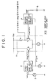
- FIG. 1 there is shown in a block diagram a basic construction of an embodiment of a video signal processing circuit to which the present invention has been applied.
- the video signal processing circuit operates in response to a timing signal (latch signal) P S/H supplied thereto from an external timing signal source 1 and delays an input video signal (original video signal) Vsigin supplied similarly from an external video signal source 2 to produce an output video signal Vsig S/H.
- the video signal processing circuit includes a first sample and hold circuit 3, a second sample and hold circuit 4, and a differential circuit 5.
- the first sample and hold circuit 3 repetitively samples and holds the input video signal Vsigin in response to the timing signal P S/H.
- the second sample and hold circuit 4 repetitively samples and holds a predetermined reference signal Vref in response to the timing signal P S/H. It is to be noted that, in the circuit arrangement shown in FIG. 1, a signal of a fixed voltage supplied from a reference signal source 6 is used as the reference signal Vref.
- the differential circuit 5 differentially processes an input video signal Vsig S/H after it has been sampled and held and a reference signal Vref S/H after it has been sampled and held, to produce an output video signal V S/H from which sample and hold noise synchronized with the timing signal P S/H has been removed.
- V S/H Vsig S/H - Vref S/H.
- the differential circuit 5 is formed of an input transistor Tr, an output transistor Tr, a load resistor R and so forth.
- the video signal processing circuit having the construction described above is incorporated as a sample and hold unit S/H into, for example, a video driver.
- the first sample and hold circuit 3 samples and holds the input video signal Vsigin to produce the video signal Vsig S/H.
- a noise ⁇ V S/H synchronized with the latch signal P S/H is superposed with the video signal Vsig S/H.
- the second sample and hold circuit 4 samples and holds the reference signal Vref to produce the reference signal Vref S/H.
- the reference signal Vref S/H includes a noise ⁇ V S/H of an equal amount superposed on the reference signal Vref.
- the differential circuit 5 thus performs differential processing between the video signal Vsig S/H and the reference signal Vref S/H to form an output video signal V S/H from which the noise ⁇ V S/H has been removed.
- FIG. 3 shows in a block diagram a basic construction of an embodiment of display apparatus to which the present invention has been applied.
- the display apparatus shown includes a display panel 11, a video driver 12, and a timing generator 13.
- the display panel 11 includes pixels arranged at intersecting points between gate lines and signal lines which extend perpendicularly to each other, and a horizontal driving circuit for distributing a plurality of video signals Vsigout (in the present example, three video signals separated to systems of the three primary RGB colors) for individual sets each including a predetermined number of (three in the present arrangement) ones of the signal lines to drive a plurality of ones of the pixels at a time.
- Vsigout in the present example, three video signals separated to systems of the three primary RGB colors
- the horizontal driving circuit operates in response to a pair of horizontal clock signals HCK1 and HCK2 and successively transfers a predetermined horizontal start signal HST to perform three pixel simultaneous driving described above.
- the display panel 11 has, in addition to the horizontal driving circuit, a built-in vertical driving circuit and line sequentially scans the gate lines.
- the vertical driving circuit operates in response to a pair of vertical clock signals VCK1 and VCK2 and successively transfers a vertical start signal VST to line sequentially select the gate lines.
- the video driver 12 relatively delays a plurality of original video signals Vsigin (in the present example, video signals of the three systems of VR, VG and VB) in accordance with an arrangement pitch of the pixels and supplies video signals Vsigout of the three RGB systems described above to the display panel 11.
- the timing generator 13 supplies timing signals such as the horizontal start signal HST and the horizontal clock signals HCK1 and HCK2 to the horizontal driving circuit of the display panel 11 to control the three pixel simultaneous driving described above. Further, the timing generator 13 supplies timing signals such as the vertical start signal VST and the vertical clock signals VCK1 and VCK2 to the vertical driving circuit of the display panel 11 to control the line sequential scanning of the gate lines. Furthermore, the timing generator 13 supplies timing signals (latch signals) such as timing signals P S/H1, P S/H2, P S/H3 and P S/H4 to the video driver 12 to control operation of the video driver 12. Consequently, the timing generator 13 can synchronously control the three pixel simultaneous driving of the display panel 11 and the delaying processing (sample and hold processing) of the video driver 12.
- FIG. 4 shows in a block diagram an example of a detailed construction of the video driver 12 shown in FIG. 3.
- the video driver 12 relatively delays the original video signals Vsigin of the three VR, VG and VG systems in accordance with the arrangement pitch of the pixels to adjust the supply timings of the video signals Vsigout of the three RGB systems to the display panel 11.
- the video driver 12 has an analog construction and includes sample and hold units S/H which perform delaying processing of the original video signals Vsigin.
- the video driver 12 includes three front stage sample and hold units S/H1, S/H2 and S/H3 corresponding to the original video signals Vsigin of the three VR, VG and VB systems.
- the video driver 12 further includes three rear stage sample and hold units S/H4 individually connected to the front stage sample and hold units S/H1, S/H2 and S/H3.
- a delay channel corresponding to the VR system is formed of a set of the front stage sample and hold unit S/H1 and a corresponding one of the rear stage sample and hold units S/H4; another delay channel corresponding to the VG system is formed of a set of the front stage sample and hold unit S/H2 and a corresponding one of the rear stage sample and hold units S/H4; and a further delay channel corresponding to the VB system is formed of a set of the front stage sample and hold unit S/H3 and a corresponding one of the rear stage sample and hold units S/H4.
- the front stage sample and hold units S/H1, S/H2 and S/H3 are controlled in synchronism with each other. It is to be noted that an amplifier AMP is connected to the output stage of each one of the delay channels.
- the original video signals Vsigin of the three VR, VG and VB systems are distributed to the three delay channels, and the video signals Vsigout of the relatively delayed three RGB systems are outputted.
- at least the three rear stage sample and hold units S/H4 have the video signal processing circuit construction shown in FIG. 1 and remove, from the output video signals Vsigout of the three RGB systems, noise originating from the sampling and holding. It is to be noted that naturally the video signal processing circuit construction shown in FIG. 1 may be adopted also for the front stage sample and hold units S/H1, S/H2 and S/H3.
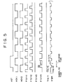
- FIG. 5 shows waveforms of various timing signals supplied from the timing generator 13 shown in FIG. 3.
- the timing generator 13 operates in response to a synchronizing signal inputted thereto from the outside and supplies the horizontal start signal HST, the horizontal clock signals HCK1, HCK2 and so forth to the display panel 11 to control driving of the display panel 11.
- the timing generator 13 additionally supplies the vertical start signal VST and the vertical clock signals VCK1 and VCK2 to the display panel 11.
- the timing generator 13 supplies a plurality of latch signals PS/H1, PS/H2, PS/H3 and PS/H4 to the sample and hold units of the video driver 12.
- the processing timings of the sample and hold units included in the delay channels of the three systems are defined by those latch signals.
- the first front stage sample and hold unit S/H1 is first caused to intermittently operate in response to the latch signal P S/H1.
- the second front stage sample and hold unit S/H2 is caused to intermittently operate in response to the latch signal P S/H2 while the third front stage sample and hold unit S/H3 is caused to continuously operate in response to the latch signal P S/H3.
- the latch signal P S/H4 is outputted so that the three rear stage sample and hold units S/H4 are caused to intermittently operate all at once.
- the potentials of the original video signals Vsigin held by the front stage sample and hold units S/H1, S/H2 and S/H3 are re-sampled at a timing at which the rear stage sample and hold units S/H4 are turned on, and are supplied to the display panel 11 side.
- the display panel 11 can simultaneously select the video signals of the three systems by horizontal switches.
- the front stage sample and hold units S/H1, S/H2 and S/H3 have phases shifted relative to each other. Accordingly, time information included in the video signals is not lost.
- the original video signals Vsigin are first sampled by the front stage sample and hold units S/H1, S/H2 and S/H3 having phases displaced from each other, and then sampled by the sample and hold units S/H4 at the rear stage so that they may be selected simultaneously at a suitable timing in the display panel.
- At least the rear stage sample and hold units S/H4 have the video signal processing circuit construction shown in FIG. 1 as described above and each produces a video signal V S/H from which noise originating from sampling and holding has been removed.
- the waveform of the video signal V' S/H when it is assumed that no noise removal is performed is indicated at the lowest stage in FIG. 5. If no countermeasure is taken, then at a timing at which the latch signal P S/H4 falls, a noise ⁇ V S/H which originates from sample and hold leakage is superposed as an offset to the original video signal Vsigin.
- the video signal V S/H exhibits a potential equal to that of the input video signal Vsigin, but during a holding period within which the latch signal P S/H4 is in an off state, the output video signal V S/H is equal to Vsigin + ⁇ V S/H.
- the video signal V S/H is amplified by the succeeding amplifier AMP, and a final output video signal Vsigout is supplied to the display panel side. Since such noise ⁇ V S/H causes a vertical stripe to appear on the display screen, in the present invention the video signal processing circuit construction shown in FIG. 1 is adopted for the rear stage sample and hold units S/H4 to remove the noise ⁇ V S/H in advance.
- FIG. 6 shows an example of a detailed construction of the display panel 11 shown in FIG. 3.
- the display panel 11 includes a pixel array section and a peripheral driving circuit section.
- the pixel array section includes liquid crystal pixels PXL arranged at individual intersecting points between gate lines X and signal lines Y which extend perpendicularly to each other.
- Each of the pixels PXL is driven by a switching element formed of a thin film transistor TFT.
- the gate electrode of the thin film transistor TFT is connected to a corresponding gate line X
- the source electrode is connected to a corresponding signal line Y
- the drain electrode is connected to a pixel electrode of a corresponding liquid crystal pixel PXL.
- an opposing electrode is disposed in an opposing relationship to each pixel electrode with a predetermined gap left therebetween, and liquid crystal is enclosed in the gap.
- the peripheral driving circuit section is divided into a vertical driving circuit 21 and a horizontal driving circuit 22.
- the vertical driving circuit 21 is connected to the gate lines X and line sequentially selects the pixels PXL of one line.
- the vertical driving circuit 21 includes a shift register, and it successively transfers the vertical start signal VST in response to the vertical clock signals VCK1 and VCK2 and outputs a gate pulse to each gate line X.
- the horizontal driving circuit 22 samples the video signals Vsigout of the three RGB systems at a time and distributes them all at once to a predetermined number of (three in the present example) ones of the signal lines Y.
- a plurality of horizontal switches HSW are interposed between the horizontal driving circuit 22 and the signal lines Y.
- Each of the horizontal switches HSW is connected commonly to three signal lines Y.
- the video signals Vsigout of the three RGB systems are sampled at a time at the three corresponding signal lines Y via the individual horizontal switches HSW.
- the horizontal driving circuit 22 successively transfers the horizontal start signal HST in response to the horizontal clock signals HCK1 and HCK2 supplied thereto from the timing generator 13 and outputs selection pulses PHSW1, PHSW2, PHSW3 In response to the selection pulses PHSW, the corresponding horizontal switches HSW are controlled to be opened or closed so that simultaneous sampling described above is performed.
- FIG. 7 illustrates in a timing chart the relationship between each of the video signals Vsigout inputted to the display panel 11 and the selection pulses PHSW.
- noise has been removed from the video signal Vsigout, and there is no problem if the selection pulses PHSW have a dispersion from one another.
- FIG. 7 a condition wherein noise is contained in the video signal Vsigout is illustrated in FIG. 7.
- the sampling timing in the display panel is the point of time of a falling edge of each of the selection pulses PHSW.
- the potentials of the video signal Vsigout sampled are different among different sets of three signal lines, and they appear as a vertical stripe on the screen.
- those signal lines Y sampled in response to the selection pulses PHSW1 and PHSW3 are held at a signal level to be used for actual writing, but those signal lines Y sampled in response to the selection pulses PHSW2 and PHSW4 exhibit a little higher signal level. This appears as a vertical stripe and deteriorates the picture quality significantly.
- sample and hold noise included in the video signal Vsigout is removed on the video driver side in advance so that, even if the selection pulses PHSW exhibit some dispersion on the display panel side, no vertical stripe will appear.
- FIG. 8 shows in circuit diagram an example of a detailed construction of the first sample and hold circuit 3 included in the video signal processing circuit (sample and hold unit S/H) shown in FIG. 1.
- the first sample and hold circuit 3 operates in response to the latch signal P S/H inputted thereto from the timing signal source 1 (such as a timing generator) and repetitively samples and holds the video signal Vsigin inputted thereto from the video signal source 2 (such as a video decoder).
- the input video signal VsigS/H after having been sampled and held is taken out via a load resistor r and a load capacitor C.
- the first sample and hold circuit 3 is formed of six transistors Q1 to Q6.
- the difference I7 (I6 - I4) between the currents I6 and I4 does not flow between the collector and the emitter of the transistor Q4, but flows to the output terminal side.
- the residual current I7 (I6 - I4) misses its escape and appears at the output terminal. Consequently, the video signal Vsig S/H exhibits different values upon sampling and upon holding, and this makes a noise ⁇ V S/H.
- the second sample and hold circuit 4 is provided in addition to the first sample and hold circuit 3, and a predetermined reference signal is repetitively sampled and held in response to the same latch signal P S/H to intentionally produce noise ⁇ V S/H of an equal amount. Then, the video signal Vsig S/H, after being sampled and held, and the reference signal, after its being sampled and held similarly, are differentially processed to remove the noise ⁇ V S/H originating from the sampling and holding. It is to be noted that, as a result of the differential processing, a DC level is added to the sample and hold video signal V S/H. However, the DC component is clamped in the video driver, and the DC offset does not matter at all.
- FIG. 10 shows in a circuit diagram an example of a detailed construction of the video signal processing circuit (sample and hold unit) shown in FIG. 1.
- the video signal processing circuit shown is applied to a set of the front stage sample and hold unit S/H1 and the corresponding rear stage sample and hold unit S/H4 constructing a channel of the R system included in the video driver 12 shown in FIG. 4.
- the front stage sample and hold unit S/H1 has an ordinary construction
- the rear stage sample and hold unit S/H4 has a noise removing function in accordance with the present invention.
- the front stage sample and hold unit S/H1 and the rear stage sample and hold unit S/H4 are connected to each other with an emitter follower 31 interposed therebetween.
- the front stage sample and hold unit S/H1 has a construction similar to that of the first sample and hold circuit 3 shown in FIG. 8.
- the front stage sample and hold unit S/H1 of the ordinary structure is formed only of the first sample and hold circuit shown in FIG. 8 and does not have a removing function for sample and hold noise at all.
- the front stage sample and hold unit S/H1 may alternatively have a sample and hold function built therein.
- the rear stage sample and hold unit S/H4 is formed of a first sample and hold circuit 3, a second sample and hold circuit 4 and a differential circuit 5.
- the first sample and hold circuit 3 and the second sample and hold circuit 4 have a basically same construction.
- the first sample and hold circuit 3 repetitively samples and holds an input video signal supplied thereto from the front stage sample and hold unit S/H1 in response to a latch signal P S/H4.
- the second sample and hold circuit 4 operates in response to the same latch signal PS/H4 and repetitively samples and holds a predetermined reference signal Vref.
- the differential circuit 5 differentially processes the video signal Vsig S/H after it has been sampled and held and the reference signal Vref S/H after it has been sampled and held, to produce an output video signal V S/H from which sample and hold noise synchronized with the latch signal P S/H4 has been removed.
- FIG. 11 illustrates in a graph a result of a simulation wherein sample and hold noise is compared in magnitude between an apparatus of the related art and apparatus according to the present invention.
- the axis of abscissa represents the input video signal Vsigin in units of volts, V
- the axis of ordinate represents the magnitude of the noise ⁇ VS/H in units of milivolts, mV.
- the input video signal Vsigin is varied stepwise for the individual three RGB systems to individually detect the noises ⁇ V S/H by simulation.
- the noise ⁇ V S/H can be reduced to approximately one fourth to one fifth with the arrangement of the present invention.
- FIG. 12 illustrates conditions of the simulation illustrated in FIG. 11. While the related art arrangement employs, for the rear stage sample and hold units S/H4, a sample and hold unit having no noise removing function, the arrangement of the present invention employs, for the rear stage sample and hold units S/H4, a sample and hold unit which has an additional noise removing function.
- noise ⁇ V S/H included in the output video signals V S/H outputted for the individual three RGB systems was detected.
- the on times of the latch signals P S/H were set to 22 nsec, and the off times were set to 44 nsec. Further, the rising time and the falling time of pulses forming the latch signals P S/H were set to 5 nsec.
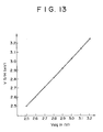
- FIG. 13 illustrates in a graph a result of a simulation of the relationship between the input video signal Vsigin and the output video signal V S/H. As seen from FIG. 13, a sufficient linearity is maintained between the input video signal Vsigin and the output video signal V S/H, and it can be seen that the processing removing sample and hold noise according to the present invention does not have any bad influence at all.
Landscapes
- Engineering & Computer Science (AREA)
- Physics & Mathematics (AREA)
- Computer Hardware Design (AREA)
- General Physics & Mathematics (AREA)
- Theoretical Computer Science (AREA)
- Chemical & Material Sciences (AREA)
- Crystallography & Structural Chemistry (AREA)
- Liquid Crystal Display Device Control (AREA)
- Control Of Indicators Other Than Cathode Ray Tubes (AREA)
- Liquid Crystal (AREA)
- Transforming Electric Information Into Light Information (AREA)
Applications Claiming Priority (2)
| Application Number | Priority Date | Filing Date | Title |
|---|---|---|---|
| JP7110182A JPH08286642A (ja) | 1995-04-11 | 1995-04-11 | 表示装置 |
| JP110182/95 | 1995-04-11 |
Publications (2)
| Publication Number | Publication Date |
|---|---|
| EP0737958A2 true EP0737958A2 (de) | 1996-10-16 |
| EP0737958A3 EP0737958A3 (de) | 1997-12-03 |
Family
ID=14529130
Family Applications (1)
| Application Number | Title | Priority Date | Filing Date |
|---|---|---|---|
| EP96400779A Withdrawn EP0737958A3 (de) | 1995-04-11 | 1996-04-11 | Videosteuerschaltung für ein Anzeigegerät |
Country Status (7)
| Country | Link |
|---|---|
| US (1) | US5936617A (de) |
| EP (1) | EP0737958A3 (de) |
| JP (1) | JPH08286642A (de) |
| KR (1) | KR100386184B1 (de) |
| MY (1) | MY112966A (de) |
| SG (1) | SG67340A1 (de) |
| TW (1) | TW418379B (de) |
Families Citing this family (18)
| Publication number | Priority date | Publication date | Assignee | Title |
|---|---|---|---|---|
| JP3517568B2 (ja) * | 1997-10-24 | 2004-04-12 | キヤノン株式会社 | 画像処理装置 |
| US6724437B2 (en) * | 1998-06-17 | 2004-04-20 | Koninklijke Philips Electronics N.V. | Method and device for adding noise to a video signal for improving a display of the video signal |
| JP2000075841A (ja) * | 1998-08-31 | 2000-03-14 | Sony Corp | 液晶表示装置 |
| US20030043139A1 (en) * | 1998-10-31 | 2003-03-06 | David W. Engler | Method and apparatus for automatic digital dc balancing for an imager of a display |
| JP3389949B2 (ja) * | 1999-03-16 | 2003-03-24 | 日本電気株式会社 | 固体撮像素子用雑音除去回路 |
| EP2273481A3 (de) | 2001-06-11 | 2012-02-22 | Genoa Color Technologies Ltd. | Einrichtung, System und Verfahren für eine Farbanzeige |
| US7714824B2 (en) | 2001-06-11 | 2010-05-11 | Genoa Color Technologies Ltd. | Multi-primary display with spectrally adapted back-illumination |
| US8289266B2 (en) | 2001-06-11 | 2012-10-16 | Genoa Color Technologies Ltd. | Method, device and system for multi-color sequential LCD panel |
| JP3982249B2 (ja) * | 2001-12-11 | 2007-09-26 | 株式会社日立製作所 | 表示装置 |
| JP4027691B2 (ja) * | 2002-03-18 | 2007-12-26 | 株式会社日立製作所 | 液晶表示装置 |
| EP1497820A4 (de) * | 2002-04-11 | 2009-03-11 | Genoa Color Technologies Ltd | Farbanzeigeeinrichtungen und verfahren mit erweiterten attributen |
| EP1590784B1 (de) | 2003-01-28 | 2008-06-04 | Genoa Color Technologies Ltd. | Subpixel-anordnung für displays mit mehr als drei primärfarben |
| KR100529076B1 (ko) * | 2003-11-10 | 2005-11-15 | 삼성에스디아이 주식회사 | 역다중화 장치 및 이를 이용한 디스플레이 장치 |
| US7193622B2 (en) * | 2003-11-21 | 2007-03-20 | Motorola, Inc. | Method and apparatus for dynamically changing pixel depth |
| JP4667904B2 (ja) * | 2005-02-22 | 2011-04-13 | 株式会社 日立ディスプレイズ | 表示装置 |
| WO2007060672A2 (en) | 2005-11-28 | 2007-05-31 | Genoa Color Technologies Ltd. | Sub-pixel rendering of a multiprimary image |
| JP2017060071A (ja) * | 2015-09-18 | 2017-03-23 | ルネサスエレクトロニクス株式会社 | 半導体装置 |
| TWI779534B (zh) * | 2020-03-25 | 2022-10-01 | 昇佳電子股份有限公司 | 電容感測電路 |
Family Cites Families (20)
| Publication number | Priority date | Publication date | Assignee | Title |
|---|---|---|---|---|
| US4004240A (en) * | 1975-02-24 | 1977-01-18 | Rca Corporation | Phase-splitter circuits |
| DE3019832C2 (de) * | 1979-05-28 | 1986-10-16 | Kabushiki Kaisha Suwa Seikosha, Shinjuku, Tokio/Tokyo | Treiberschaltung für eine Flüssigkristallanzeigematrix |
| JPS5819798A (ja) * | 1981-07-28 | 1983-02-04 | Sony Corp | サンプルホ−ルド回路 |
| EP0167408B1 (de) * | 1984-07-06 | 1991-06-12 | Sharp Kabushiki Kaisha | Steuereinrichtung für ein Flüssigkristallfarbanzeigegerät |
| JPS61121081A (ja) * | 1984-11-19 | 1986-06-09 | キヤノン株式会社 | 液晶表示パネル |
| US4803554A (en) * | 1987-09-30 | 1989-02-07 | Polaroid Corporation | Electronic imaging camera utilizing EPROM memory |
| JPH0750135B2 (ja) * | 1989-07-14 | 1995-05-31 | 三菱電機株式会社 | ピークホールド回路 |
| US4947169A (en) * | 1989-10-24 | 1990-08-07 | Burr-Brown Corporation | Dummy/trim DAC for capacitor digital-to-analog converter |
| JPH03225868A (ja) * | 1990-01-30 | 1991-10-04 | Hitachi Ltd | 固体撮像素子とそれを用いた撮像装置 |
| JPH04147498A (ja) * | 1990-10-09 | 1992-05-20 | Nec Corp | サンプルホールド回路 |
| DE69221434T2 (de) * | 1991-11-15 | 1997-12-11 | Asahi Glass Co Ltd | Bildanzeigevorrichtung und Verfahren zu ihrer Steuerung |
| US5406329A (en) * | 1992-01-08 | 1995-04-11 | Ikegami Tsushinki Co., Ltd. | Solid state image pickup apparatus having test signal generator |
| JP2777302B2 (ja) * | 1992-01-16 | 1998-07-16 | 株式会社東芝 | オフセット検出回路、出力回路および半導体集積回路 |
| EP0554051A1 (de) * | 1992-01-31 | 1993-08-04 | Canon Kabushiki Kaisha | Bildanzeigevorrichtung mit monokristalliner Siliziumschicht, Herstellungsverfahren und Ansteuerungsverfahren hierfür |
| GB9207527D0 (en) * | 1992-04-07 | 1992-05-20 | Philips Electronics Uk Ltd | Multi-standard video matrix display apparatus and its method of operation |
| JP3042159B2 (ja) * | 1992-04-10 | 2000-05-15 | ソニー株式会社 | Ccd素子の欠陥画素補正回路 |
| JPH05328268A (ja) * | 1992-05-27 | 1993-12-10 | Toshiba Corp | 液晶表示装置 |
| US5515103A (en) * | 1993-09-30 | 1996-05-07 | Sanyo Electric Co. | Image signal processing apparatus integrated on single semiconductor substrate |
| JPH07264491A (ja) * | 1994-03-24 | 1995-10-13 | Sharp Corp | 固体撮像装置の出力回路 |
| US5572155A (en) * | 1994-06-20 | 1996-11-05 | Fuji Photo Film Co., Ltd. | CCD signal read-out circuit free from ailiasing of high-frequency noises |
-
1995
- 1995-04-11 JP JP7110182A patent/JPH08286642A/ja active Pending
-
1996
- 1996-04-03 US US08/627,004 patent/US5936617A/en not_active Expired - Lifetime
- 1996-04-08 KR KR1019960010394A patent/KR100386184B1/ko not_active Expired - Fee Related
- 1996-04-09 SG SG1996007822A patent/SG67340A1/en unknown
- 1996-04-09 MY MYPI96001338A patent/MY112966A/en unknown
- 1996-04-10 TW TW085104213A patent/TW418379B/zh not_active IP Right Cessation
- 1996-04-11 EP EP96400779A patent/EP0737958A3/de not_active Withdrawn
Also Published As
| Publication number | Publication date |
|---|---|
| EP0737958A3 (de) | 1997-12-03 |
| TW418379B (en) | 2001-01-11 |
| JPH08286642A (ja) | 1996-11-01 |
| US5936617A (en) | 1999-08-10 |
| MY112966A (en) | 2001-10-31 |
| SG67340A1 (en) | 1999-09-21 |
| KR100386184B1 (ko) | 2003-08-19 |
| KR960038717A (ko) | 1996-11-21 |
Similar Documents
| Publication | Publication Date | Title |
|---|---|---|
| US5936617A (en) | Display apparatus | |
| JP4472155B2 (ja) | 液晶表示装置用データドライバ | |
| US4779085A (en) | Matrix display panel having alternating scan pulses generated within one frame scan period | |
| US6356253B2 (en) | Active-matrix display device and method for driving the display device to reduce cross talk | |
| US6512505B1 (en) | Liquid crystal display apparatus, its driving method and liquid crystal display system | |
| EP0382567B1 (de) | Flüssigkristallanzeigeeinheit und Steuerverfahren dafür | |
| US6624800B2 (en) | Controller circuit for liquid crystal matrix display devices | |
| US4795239A (en) | Method of driving a display panel | |
| US5801673A (en) | Liquid crystal display device and method for driving the same | |
| US5604513A (en) | Serial sampling video signal driving apparatus with improved color rendition | |
| US7580018B2 (en) | Liquid crystal display apparatus and method of driving LCD panel | |
| US20080106534A1 (en) | Display apparatus | |
| US4789899A (en) | Liquid crystal matrix display device | |
| US20010040548A1 (en) | LCD and method for driving same | |
| JP3633151B2 (ja) | アクティブマトリクス表示装置およびその駆動方法 | |
| EP0071911A2 (de) | Anzeigeeinrichtung mit einem Multiplex-Rasterbildschirm | |
| US6177917B1 (en) | Liquid crystal display device and method for driving the same | |
| JP2003330423A (ja) | 液晶表示装置及びその駆動制御方法 | |
| JP3341530B2 (ja) | アクティブマトリクス表示装置 | |
| JP2835254B2 (ja) | 表示装置の駆動回路 | |
| JPH0458036B2 (de) | ||
| JP2630317B2 (ja) | 液晶装置及びその駆動方法 | |
| JP2003150126A (ja) | 表示駆動装置 | |
| JPH05100637A (ja) | 液晶表示装置の駆動法 | |
| JPH0713523A (ja) | 液晶駆動方法と液晶表示装置 |
Legal Events
| Date | Code | Title | Description |
|---|---|---|---|
| PUAI | Public reference made under article 153(3) epc to a published international application that has entered the european phase |
Free format text: ORIGINAL CODE: 0009012 |
|
| AK | Designated contracting states |
Kind code of ref document: A2 Designated state(s): DE FR GB NL |
|
| PUAL | Search report despatched |
Free format text: ORIGINAL CODE: 0009013 |
|
| AK | Designated contracting states |
Kind code of ref document: A3 Designated state(s): DE FR GB NL |
|
| 17P | Request for examination filed |
Effective date: 19980514 |
|
| STAA | Information on the status of an ep patent application or granted ep patent |
Free format text: STATUS: THE APPLICATION IS DEEMED TO BE WITHDRAWN |
|
| 18D | Application deemed to be withdrawn |
Effective date: 20041102 |