EP0738883B1 - Transducteur à ultrason intégré avec un amplificateur réglable - Google Patents
Transducteur à ultrason intégré avec un amplificateur réglable Download PDFInfo
- Publication number
- EP0738883B1 EP0738883B1 EP96105227A EP96105227A EP0738883B1 EP 0738883 B1 EP0738883 B1 EP 0738883B1 EP 96105227 A EP96105227 A EP 96105227A EP 96105227 A EP96105227 A EP 96105227A EP 0738883 B1 EP0738883 B1 EP 0738883B1
- Authority
- EP
- European Patent Office
- Prior art keywords
- amplifier
- amplifier device
- capacitive component
- transfer
- transducer head
- Prior art date
- Legal status (The legal status is an assumption and is not a legal conclusion. Google has not performed a legal analysis and makes no representation as to the accuracy of the status listed.)
- Expired - Lifetime
Links
- 238000012546 transfer Methods 0.000 claims description 121
- 238000002604 ultrasonography Methods 0.000 claims description 45
- 230000005669 field effect Effects 0.000 claims description 9
- 230000001419 dependent effect Effects 0.000 claims description 5
- 238000012545 processing Methods 0.000 claims description 5
- 230000005540 biological transmission Effects 0.000 description 100
- 230000003321 amplification Effects 0.000 description 8
- 238000003199 nucleic acid amplification method Methods 0.000 description 8
- 239000003990 capacitor Substances 0.000 description 6
- 238000010586 diagram Methods 0.000 description 5
- 230000004044 response Effects 0.000 description 5
- 238000003491 array Methods 0.000 description 4
- 230000008859 change Effects 0.000 description 4
- 238000003384 imaging method Methods 0.000 description 4
- 230000001939 inductive effect Effects 0.000 description 2
- 230000003287 optical effect Effects 0.000 description 2
- 230000002787 reinforcement Effects 0.000 description 2
- 230000036962 time dependent Effects 0.000 description 2
- 230000008901 benefit Effects 0.000 description 1
- 230000008878 coupling Effects 0.000 description 1
- 238000010168 coupling process Methods 0.000 description 1
- 238000005859 coupling reaction Methods 0.000 description 1
- 238000013016 damping Methods 0.000 description 1
- 230000001066 destructive effect Effects 0.000 description 1
- 238000011161 development Methods 0.000 description 1
- 230000018109 developmental process Effects 0.000 description 1
- 239000003814 drug Substances 0.000 description 1
- 238000005516 engineering process Methods 0.000 description 1
- 238000011156 evaluation Methods 0.000 description 1
- 230000010354 integration Effects 0.000 description 1
- 238000012886 linear function Methods 0.000 description 1
- 238000000034 method Methods 0.000 description 1
- 238000013021 overheating Methods 0.000 description 1
- 230000000630 rising effect Effects 0.000 description 1
- 238000010079 rubber tapping Methods 0.000 description 1
- 239000004065 semiconductor Substances 0.000 description 1
- 238000000527 sonication Methods 0.000 description 1
- 239000000758 substrate Substances 0.000 description 1
- 238000004154 testing of material Methods 0.000 description 1
Images




Classifications
-
- B—PERFORMING OPERATIONS; TRANSPORTING
- B06—GENERATING OR TRANSMITTING MECHANICAL VIBRATIONS IN GENERAL
- B06B—METHODS OR APPARATUS FOR GENERATING OR TRANSMITTING MECHANICAL VIBRATIONS OF INFRASONIC, SONIC, OR ULTRASONIC FREQUENCY, e.g. FOR PERFORMING MECHANICAL WORK IN GENERAL
- B06B1/00—Methods or apparatus for generating mechanical vibrations of infrasonic, sonic, or ultrasonic frequency
- B06B1/02—Methods or apparatus for generating mechanical vibrations of infrasonic, sonic, or ultrasonic frequency making use of electrical energy
- B06B1/0207—Driving circuits
-
- H—ELECTRICITY
- H03—ELECTRONIC CIRCUITRY
- H03G—CONTROL OF AMPLIFICATION
- H03G1/00—Details of arrangements for controlling amplification
- H03G1/0005—Circuits characterised by the type of controlling devices operated by a controlling current or voltage signal
- H03G1/0035—Circuits characterised by the type of controlling devices operated by a controlling current or voltage signal using continuously variable impedance elements
- H03G1/0052—Circuits characterised by the type of controlling devices operated by a controlling current or voltage signal using continuously variable impedance elements using diodes
- H03G1/0064—Variable capacitance diodes
-
- H—ELECTRICITY
- H03—ELECTRONIC CIRCUITRY
- H03G—CONTROL OF AMPLIFICATION
- H03G3/00—Gain control in amplifiers or frequency changers
Definitions
- the invention relates to an ultrasonic transducer head and an ultrasound device with such a transducer head.
- the Ultrasonic transducer head comprises at least one transducer element, which receives ultrasound signals and into electrical reception signals converts, as well as an amplifier device that the Received signals of the converter element are electrically amplified.
- an ultrasonic transducer head is from EP-A-0 600 654 known.
- ultrasound devices for imaging objects with Ultrasound using the pulse-echo method is known mainly in medicine for imaging tissue and in non-destructive material testing.
- the converter head contains at least one piezoelectric transducer element, but generally a variety of transducer elements, that form a linear or two-dimensional array.
- the converter elements in the converter head are in a transmission mode of the ultrasound device through electrical transmission pulses of a transmitter excited to high frequency vibrations and generate an ultrasound pulse directed at the object. This ultrasound pulse is applied to the object, for example Interfaces between two media of different acoustic Impedance reflected.
- These receive signals are converted from the converter head via appropriate signal cables transmitted to a main frame. Be in the main unit the transmitted received signals of each transducer element from a preamplifier assigned to this converter element strengthened.
- the amplified received signals become one Signal processing unit in the main unit for evaluating the Information about the depicted object is supplied.
- a problem with such ultrasound devices is the high dynamics of the reception signals during reception operation.
- TGC amplifiers time-dependent gain control
- each transducer element in the transducer head is assigned an amplifier with controllable gain (variable gain amplifier) in addition to a preamplifier with constant gain.
- the pre-amplifier with a predetermined gain is electrically connected between the converter element and the controllable amplifier.
- the output of the controllable amplifier is formed with a push-pull emitter follower as an impedance converter and is electrically connected to the associated signal cable, which transmits the amplified received signals to a main device.
- the input impedance of the preamplifier is matched to the high impedance of the transducer element, while the output impedance of the push-pull emitter follower is matched to the lower impedance of the signal cable.
- the amplified received signals are used to build up an image of the object.
- the controllable amplifier is controlled by the main unit via additional lines in the signal cable with control signals (TGC control signals) for controlling the amplification of the controllable amplifier in order to compensate for time-dependent damping.
- TGC control signals control signals for controlling the amplification of the controllable amplifier in order to compensate for time-dependent damping.
- the controllable compensation amplifiers TGC amplifiers
- the controllable amplifiers in this converter head known from EP - A - 0 600 654 function according to the principle of a steepness multiplier, which is known, for example, from Tietze, Schenk: "Semiconductor circuit technology", 9th edition, 1990, Springer Verlag, p. 350 .
- the quiescent current of the entire circuit must be dimensioned such that the ultrasound received signal with the highest amplitude is also transmitted without distortion.
- the controllable amplifiers in the ultrasound device known from EP - A - 0 600 654 therefore have a comparatively high power loss.
- An operational amplifier with a controllable amplification in which a field effect transistor (FET) controllable by a continuously or digitally controllable control voltage source is connected to a negative feedback circuit for the operational amplifier.
- a feedback circuit with a further operational amplifier for linearizing the electrical resistance of the FET is additionally provided for the FET as a controllable resistor.
- the FET can also be connected to a negative feedback to increase its dynamic range ( "Application Note 200-1, Designer's Guide for 200 Series Op Amps" from Comlinear Corporation, November 1984 ).
- FETs as controllable resistors do not require any control power, but they have comparatively high tolerances in their characteristic curves.
- the invention is therefore based on the object of an ultrasonic transducer head with at least one transducer element and with a controllable amplifier device for each transducer element and an ultrasound device with one Specify transducer head where the gain of each amplifier device is controllable and at the same time the power loss each amplifier device is kept low. at a one-dimensional or two-dimensional array of transducer elements in the transducer head they should be the transducer elements each associated amplifier devices also good Have synchronism properties.
- the invention is based on the consideration, the amplification of the Control amplifier device by controlling a capacitance. Such a capacitive control is practical negligible power consumption.
- the amplifier device based on this consideration, contains at least one capacitive component, the capacity of which is controllable and determines the gain of the amplifier device.
- a controllable capacitive component is preferably one Capacitance diode provided. Capacitance diodes are over one control voltage applied in the reverse direction is practically lossless controllable and precisely reproducible Characteristic curves on.
- this is at least one capacitive component in a negative feedback circuit for switched at least one amplifier.
- a particularly advantageous embodiment is based on the further consideration, the electrical reception signal of the transducer element two in succession in the amplifier device Transmission links with different frequency-dependent Feed transfer functions and the two transfer functions to choose or adjust so that their frequency dependencies in a given frequency range substantially compensate for the received signals and the amplitude of the amplified output signal of the amplifier device versus the amplitude of the input signal an essentially frequency-independent gain having.
- the gain for the electrical received signal is then changed by changing the frequency dependence of the two Transfer functions in the specified frequency range controlled.
- the amplifier device contains in this embodiment two electrical Transmission elements, each with a frequency-dependent Transfer function.
- the transfer function is included defined as the ratio of the amplitude of the output signal to the Amplitude of the input signal of the respective transmission element.
- the two transmission links are between one Input of the amplifier device for applying the one to be amplified electrical received signal and an output of Amplifier device for tapping the amplified electrical Received signal connected in series.
- At least one of the two transmission elements contains at least one controllable capacitive component.
- the frequency dependencies the transfer functions of the two transfer elements are chosen so that the two corresponding logarithmic Transfer functions in the area of one edge each essentially linear depending on a bijective function of the frequency.
- the logarithmic transfer function is proportional to the logarithm of the amount in general complex transfer function to a given real basis.
- the logarithmic transfer function one of the two transmission links has a positive one Slope with a positive slope while the logarithmic Transfer function of the other transmission link has a negative edge with a negative edge Pitch.
- the slopes of the two flanks of the logarithmic In terms of amount, transfer functions are at least chosen approximately the same.
- the flanks of the two logarithmic Transfer functions are now relative to each other slidable within the frequency range of the received signals. By moving the flanks against each other the Gain of the amplifier device controlled.
- the ultrasound device contains control means that at least with the transmission element that is the capacitive component contains, are in operative connection.
- the tax revenue can only flank to smaller or larger frequencies move towards it while the other flank remains unchanged remains, or shift both flanks at the same time.
- the transmission element with the positive edge can be at least one element from one High pass at least first order, a differentiator and a pre-emphasis group of electrical Circuits or networks included.
- the transmission link with the negative edge at least one element from the one low pass at least first Order, comprising an integrator and a de-emphasis member Group of electrical circuits or networks contain.
- Such transmission elements can in particular with negative feedback amplifiers can be realized.
- the ultrasonic transducer head shown in FIG. 1, designated 9 contains at least one converter element 1 and an amplifier device 2 for amplifying the received signals S des Converter element 1. To an input 2A of the amplifier device 2, the received signals S of the converter element 1 are applied. The amplified received signals can be at an output 2B of the amplifier device 2 are tapped and are denoted by S '.
- the gain A * of Amplifier device 2 is of the capacitance C of the controllable capacitive component 23 dependent.
- To control the Capacitance C of the capacitive component 23 and thus the gain A * of the amplifier device 2 is at least a capacitive component 23 via a dashed line Active connection line 8 connected to control means 5.
- the active connection line 8 can then accordingly with an electrical connection or an optical coupler or an inductive coupler or a piezo coupler.
- the control means 5 are generally arranged outside the transducer head 9, can, however, also be at least partially integrated in the converter head 9 his.
- the transducer element 1 is preferably part of an ultrasound array (not shown in FIG. 1) with several Transducer elements.
- the array can be linear or also a two-dimensional, for example matrix-shaped array his. Such arrays are generally in a substrate integrated through microstructuring. Every converter element of the array is then a controllable amplifier device for Amplify the received signals of the transducer element. The amplifier devices are together with the transducer elements of the array integrated in the converter head.
- the transducer head 9 can only be used to receive ultrasound or also for both sending and receiving ultrasound be provided.
- the ultrasound device for imaging a - not shown - Object with ultrasound contains one Transducer head 9 for both sending and receiving Ultrasound with an array of transducer elements 1 and each a controllable amplifier device 2 for each Transducer element 1.
- a transmitter 30 transmits via transmission lines 33 Transmitting pulses for driving each transducer element 1 that are that the transducer elements 1 to ultrasonic vibrations be stimulated.
- the duty cycle of an individual Transmitting pulse can generally be between 50 ns and 500 ns, preferably around 150 ns, and the pulse height (amplitude) of the transmission pulses between 50 and 150 V.
- All transducer elements 1 of the array are preferred controlled by the transmitter 30 to generate a delay a preferably focusable ultrasound beam which is directed onto the object is directed (electronic scan).
- a Converter head with only a single converter element 1 will In contrast, the object is mechanically scanned by moving the transducer element 1 (mechanical scan).
- the transducer element 1 mechanical scan.
- a receiving company of the ultrasound device are those from the object to the transducer elements 1 reflected ultrasound pulses in each Converter element 1 converted into electrical received signals S.
- These received signals S are in the converter head 9 from the associated amplifier device 2 amplified, and the amplified Received signals S 'are transmitted via signal lines 34 signal processing means 31 for building an image of the Object supplied.
- the impedances of the amplifier devices 2 are preferably at least approximately the impedances the assigned signal lines 34 adapted.
- each Transducer element 1 is preferably a duplexer 32 for switching between transmit mode and receive mode.
- On first part 32A of duplexer 32 connects in the transmission mode the associated transducer element 1 with the transmitter 30 and decoupled in reception mode, the transmitter 30 both from the Amplifier device 2 as well as from the converter element 1.
- a second part 32B of the duplexer 32 connects this Transducer element 1 in reception mode with the amplifier device 2 and decouples the transmission in general sensitive amplifier device 2 'on the one hand by the transmitter 30 to protect against its transmission pulses and the other from the Transducer element 1.
- the transducer element 1 and the two parts 32A and 32B of duplexer 32 are in common Switching point electrically connected. At least the one in between Converter element 1 and the input 2A of the associated amplifier device 2 arranged second part 32 B of each duplexer 32 is with the transducer element 1 and the amplifier device 2 integrated in the converter head 9.
- the first part 32A can also be arranged in the converter head 9 as shown.
- For the Duplexers 32 can control lines, not shown, for Switching between transmit and receive mode provided his.
- Each amplifier device 2 contains at least one controllable one capacitive component 23.
- Any controllable capacitive Component 23 is preferably a common electrical Control line 8 as an active connection line with the Control means 5 connected.
- the capacitive components 23 are driven by a common control signal CS Controlling the gains A * of the amplifier devices 2.
- This embodiment with a common control of all Amplifier devices 2 is particularly advantageous in essentially identical to each other Converter elements 1 and amplifier devices 2 in the converter head 9.
- the amplifier devices 2 can also be any for itself via one or more control lines or active connection lines 8 in operative connection with the control means 5 stand for independent control of the reinforcements A * Amplifier devices 2.
- the operative connection between amplifier devices 2 and control means 5 instead by electrical means again on one of the other described Ways.
- the amplifier device 2 contains in an advantageous Embodiment at least one amplifier, the input is connected to the converter element 1 and its output with is connected to the output 2B of the amplifier device 2. additionally is a negative feedback circuit for the least provided an amplifier. With only one amplifier the output of the amplifier is connected to its input. On Part of the amplifier's output signal is fed back to the input and the input signal of the amplifier in phase opposition superimposed so that the effective input signal is weakened becomes. With several amplifiers connected in series can create a negative feedback circuit for each one Amplifier can be provided or a negative feedback circuit over at least two and preferably all successive ones Amplifier or a combination of such individual and multiple negative feedbacks can be provided.
- the negative feedback circuit contains at least one amplifier the at least one controllable capacitive component 23 Change the capacitance C of the at least one capacitive Component 23 then has a change in the degree of negative feedback and thus the gain A * of the amplifier device 2 for Episode.
- a first exemplary embodiment of an amplifier device 2 with a negative feedback amplifier is shown in FIG.
- a field effect transistor 6 is provided as an amplifier with a gate CG, a source SC and a drain D.
- the gate CG of the field effect transistor 6 is connected to the input 2A of the amplifier device 2.
- the source SC of the field effect transistor 6 is connected to a capacitance diode as a capacitive component 23.
- the drain D forms the output of the amplifier and is connected on the one hand via a capacitance 27 to the output 2B of the amplifier device 2 and on the other hand via a resistor 26 with a positive drain voltage U 0 .
- the capacitance diode 23 is connected via a control line 8 to a control voltage source as control means 5, which biases the capacitance diode 23 in the reverse direction with a reverse voltage U C.
- a control voltage source as control means 5
- the output signal of the field effect transistor 6 is partially fed back to its input signal. Therefore, if the capacitance C of the capacitance diode 23 is changed by controlling the reverse voltage U C , the degree of negative feedback of the amplifier 6 and thus the gain A * of the amplifier device 2 change.
- the negative feedback with the capacitive component 23 and the gain of the amplifier device 2 are due the influence of the capacitance C of the capacitive component 23 as a function of frequency, in the case shown in the form of a high-pass behavior.
- a resistor 29 for fixing the gate potential at the gate CG of the field-effect transistor 6 and a resistor 28 are preferably also provided, which causes the output signal which is used for the negative feedback to also occur at the source SC.
- the amplifier device 2 becomes the gain A * of the amplifier device 2 by controlling the capacitance C at least a capacitive component 23, but essentially controlled independently of frequency.
- This embodiment will 4 to 16 described in more detail.
- the amplifier device 2 comprises a first transmission link 3 with a generally complex Transfer function G ', a second transfer element 4 with a generally complex transfer function H '.
- the first transmission element 3 and the second transmission element 4 are between the input 2A and the output 2B of the amplifier device 2 electrically connected in series. That to be reinforced electrical received signal S of the converter element 1 is applied to the input 2A of the amplifier device 2 and supplied to the first transmission element 3.
- In the first Transmission element 3 becomes the received signal S with the transfer function G 'of the first transmission element 3 multiplied.
- ) and H log a (
- At least one of the two transmission elements 3 or 4 contains at least one controllable capacitive component 23.
- the control means 5 are available with each of these controllable capacitive Components 23 in the amplifier device 2 in Operatively connected. In the example in FIG. 4, the control means 5 only with a capacitive component in the transmission element 4 connected via the dashed line 8.
- the control means 5 control each connected to them capacitive component 23 in the transmission element 3 or 4, that the transfer function G 'or H' of this transfer element 3 or 4 changed in their frequency dependence becomes. The exact functioning of this control will explained below.
- the corresponding rectangular gain control area predetermined by the intervals ⁇ f and ⁇ A is hatched and designated by 10.
- the minimum logarithmic gain A min is generally chosen to be greater than or equal to 0, but can also be less than 0.
- the maximum gain A max can also be less than 0. In these cases, the amplitude of the output signal S 'of the amplifier device 2 is smaller than the amplitude of the input signal S.
- the logarithmic transfer functions G log a (
- ) and H log a (
- the first real transmission parameter m ⁇ 0 gives the amount of the slopes
- the logarithmic transfer function G of the transmission element 3 thus has a linear edge with the slope -m in the associated frequency range, while the logarithmic transfer function H of the second transmission element 4 has a linear edge with the slope + m in its assigned frequency range.
- the slopes of the two flanks differ in their algebraic signs, but have the same magnitude.
- At least for frequencies f from the frequency range ⁇ f or for function values ⁇ (f) from the corresponding, unambiguous certain value range ⁇ is the logarithmic gain A - and of course the complex reinforcement A * - the amplifier device 2 thus at least approximately frequency-independent.
- This practically frequency-independent value of the logarithmic gain A according to equation (4) can now be changed by suitable setting of at least one of the transmission parameters m, ⁇ G and ⁇ H of the two logarithmic transmission functions G and H in a manner suitable for a specific application of the amplifier device 2 ,
- the gain variation ⁇ A of the amplifier device 2 which can be achieved in this way depends on the variation ⁇ m of the amount m of the slopes of the two logarithmic transfer functions G and H in the region of their edges and / or the variation ⁇ G of the transfer parameter ⁇ G of the edge of the logarithmic transfer function G and / or Variation ⁇ H of the transfer parameter ⁇ H of the flank of the logarithmic transfer function H.
- the variations ⁇ G and ⁇ H correspond to a shift in the flank of the associated logarithmic transfer function G and H.
- the variation ⁇ m corresponds to a change in the absolute steepness of both flanks.
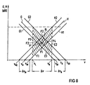
- FIGS. 6 to 8 show exemplary embodiments with the aid of diagrams how the logarithmic gain A of the amplifier device 2 can be controlled by varying the logarithmic transfer functions G and H of the two transfer elements 3 and 4.
- the decimal logarithmic amplification or transfer function that is common in electronics is described without restriction of generality
- a / dB 20 log (
- G / dB 20 log (
- ) H / dB 20 log (
- ) with the logarithm log: log 10 used for base 10.
- the transmission parameter ⁇ G corresponds to the value of ⁇ at which the elongated edge E intersects the abscissa.
- the edge E of the logarithmic transfer function G is kept constant during the operation of the amplifier device 2.
- the logarithmic transfer function H of the second transfer element 4 has a flank F which rises linearly with increasing ⁇ in accordance with the relationship (3b) with the gradient + m> 0 and which, from a certain functional limit value ⁇ 3, into a substantially constant part of the logarithmic transfer function H. transforms.
- This logarithmic transfer function H corresponds to the characteristic curve of a high pass as a transfer element 4.
- the edge F of the logarithmic transfer function H can now be shifted between two edges labeled F1 and F2 of two corresponding logarithmic transfer functions H1 and H2 with the same slope + m.
- the transfer parameter ⁇ H of the logarithmic transfer function H is varied in the interval limited by the two transfer parameters ⁇ H1 and ⁇ H2 of the two logarithmic transfer functions H1 and H2 with ⁇ H1 ⁇ H2 .
- the transmission parameters ⁇ H , ⁇ H1 and ⁇ H2 correspond to the values of ⁇ at which the extended flank F, F1 and F2 intersect the abscissa.
- the associated logarithmic transfer function H, H1 or H2 assumes a predetermined value, for example again 0 dB.
- the slope of the logarithmic transfer function H defined by the transfer parameter + m remains unchanged when the edge F is shifted.
- the flank F of the logarithmic transfer function H is in the hatched area over a functional value range ⁇ lying between the function limit value ⁇ 0 of the logarithmic transfer function G of the low pass as the left function value ⁇ L and the smallest function limit value ⁇ 1 of the logarithmic transfer function H of the high pass as the right function value ⁇ R Area displaceable relative to the edge E of the logarithmic transfer function G.
- the intersection P between the two edges E and F lies on the edge E between the two extreme intersections P1 of the edge F1 with the edge E and P2 of the edge F2 with the edge E.
- the logarithmic gain A of the amplifier device 2 can be graphically a double value one of the two logarithmic transfer functions G or H can be determined at this intersection point P.
- the maximum value A max of the logarithmic gain A corresponds to the intersection P1, the minimum value A min, however, to the intersection P2.
- the logarithmic transfer function H is now kept constant with the edge F with a positive slope (positive edge), while the logarithmic transfer function G is varied with the edge E with a negative slope (negative edge).
- the transfer parameter f H of the logarithmic transfer function H thus remains constant.
- the transfer parameter f G of the logarithmic transfer function G is controlled between the two transfer parameters f G2 and f G1 by two logarithmic transfer functions G2 and G1 with f G2 ⁇ f G1 .
- the edge E of the logarithmic transfer function G can thus be shifted with an unchanged slope m between the two edges E2 and E1 of the two logarithmic transfer functions G2 and G1 in a frequency range ⁇ f between a left corner frequency f L and a right corner frequency f R with f L ⁇ f R.
- the variation range of the edge E over the frequency range ⁇ f is hatched again.
- intersection P of the two flanks E and F varies between the intersection P2 of the edge E2 with the edge F and the intersection P1 of the edge E1 with the edge F.
- the resulting logarithmic gain A of the amplifier device 2 again corresponds to twice the logarithmic value Transfer function G or H at the intersection P.
- the logarithmic transfer function G can again be implemented with a transfer element 3 with a low-pass character.
- a variation ⁇ f G of the transmission parameter f G from f G2 to f G1 then also corresponds to a variation of the cutoff frequency of the low pass from f 2 to f 1 .
- the logarithmic transfer function H shown has a continuous edge F and can be implemented, for example, with a differentiator in the transfer element 4.
- the edges E and F of both logarithmic transfer functions G and H can now be shifted within the predetermined function value interval ⁇ .
- the transmission parameter ⁇ G of the logarithmic transmission function G of the first transmission element 3 is controlled in the variation interval limited by the two transmission parameters ⁇ G1 and ⁇ G2 of the two logarithmic transmission functions G1 and G2 with ⁇ G1 ⁇ G2 .
- the corresponding variation ranges of the flanks E and F over the interval ⁇ are hatched in each case.
- the intersection P of the two flanks E and F lies in the double-hatched, parallelogram-shaped area 15 with the four corner points P1, P2, P3 and P4.
- the vertex P1 is the intersection of the two flanks E1 and F1
- the vertex P2 is the intersection of the flanks E2 and F2
- the vertex P3 is the intersection of the flanks E1 and F2
- the vertex P4 is the intersection of the flanks E2 and F1.
- the variation ⁇ A of the gain A when the two transfer parameters ⁇ G and ⁇ H are varied is therefore equal to the sum of the individual variations ⁇ A according to the equations (7 ) or (6).
- the gain variation ⁇ A when shifting both flanks E and F by changing their associated transmission parameter ⁇ G or ⁇ H is twice as large as with variation of only one transmission parameter ⁇ G or ⁇ H , ie only when shifting an edge E or F.
- a transmission link with a positive edge such as the edge F in FIGS. 6 to 8 can preferably with the help of an nth order high pass with n ⁇ 1, one Differentiator or a preemphasis become.
- a transmission link with a negative edge like contains, for example, the edge E in FIGS. 6 to 8 preferably a low-pass n-th order with n ⁇ 1 Integrator or a de-emphasis element.
- each Transmission link preferably comprises at least in each case an amplifier for adjusting the absolute size of the associated transfer function.
- Amplifier device 2 also has at least one amplifier one that is frequency-independent at least in the frequency range ⁇ f Gain included, the electrical in series to the two Transmission elements 3 and 4 is switched.
- the examples given for the transmission elements 3 and 4 The amplifier device 2 are numerous to the person skilled in the art known from embodiments. 9 to 14 show simple basic circuits for such transmission elements. All transmission elements shown contain a negative feedback Amplifier 20 with one input 20A and one Output 20B and a capacitive component 23. The input the transmission link corresponds to point 40, and the output of the transmission link corresponds to point 50. The Node 50 is at output 20B of amplifier 20 electrically connected.
- the input 20A of the amplifier 20 is connected to the output 20B of the amplifier 20 via a first electrical resistor 21 fed back.
- a minus sign at the input 20A of the amplifier 20 should indicate that the fed back part of the output signal the input signal reduced, i.e. there is negative feedback.
- An input signal at the input 40 of the high pass is via a series connection a second electrical resistor 22 and controllable capacitive component 23 to the input 20A of the amplifier 20 switched.
- the cutoff frequency of the high pass is now proportional to 1 / (RC) with the size R of the second electrical resistance 22 and the capacitance C of the capacitive component 23.
- a n-th order high pass n> 1 can be done simply by connecting n high passes in series first order.
- the slope of the rising corresponds to the positive edge of the n-th order high pass the n-fold slope of the positive flank of the high pass first order.
- the gain variation can thus be ordered for a transmission element ⁇ A of the amplifier device 2 accordingly multiply.
- FIG. 10 shows an embodiment of a differentiating element (Differentiator).
- the output 20B of the amplifier 20 is with electrically connected to the input 20A via the resistor 21. between these negative feedback input 20 A of the amplifier and the input 40 of the differentiator is capacitive Component 23 switched.
- This differentiator is obtained from the basic circuit for the high-pass filter shown in FIG. 9 Omission of the second resistor 22.
- the differentiator has no cutoff frequency.
- the output 20B of the Amplifier 20 again through the first resistor 21 with the Input 20A of amplifier 20 is fed back.
- the entrance 40 of the pre-emphasis element is now via a parallel connection of the second resistor 22 and the capacitive component 23 with electrically connected to the input 20A of the amplifier 20.
- the cutoff frequency of the pre-emphasis element is proportional to 1 / (RC), where R is the ohmic resistance of the second resistor 22 and C the electrical capacitance of the capacitive Component 23 are.
- FIG. 12 shows an embodiment of a low pass first Order shown.
- the output 20B of the amplifier 20 is via a parallel connection of the first resistor 21 and the capacitive component 23 with the input 20A of the amplifier 20 electrically connected.
- the input 40 of the low pass is via the second resistor 22 to the input 20A of the Amplifier 20 electrically connected.
- the cutoff frequency of the Low pass is proportional to 1 / (RC) with the size R of the first electrical resistance 21 and the capacitance C of the capacitive component 23.
- a n-th order low pass n> 1 can be done simply by connecting n low passes in series first order.
- the slope of the falling negative edge of the n-th order low pass corresponds to the n-fold slope of the negative edge of the First order low pass.
- FIG. 13 shows an embodiment of an integrating element (Integrators) illustrates. Output 20B and input 20A of the amplifier 20 are via the capacitive component 23 electrically coupled. In front of the input 20A of the amplifier 20, the resistor 22 is switched. The integrator 13 can by omitting the resistor 21 in the transmission element 12 can be obtained. A cut-off frequency does not have the integrator.
- FIG 14 shows a basic circuit of a Deemphasis limb as a transmission limb.
- the input 20A of the amplifier 20 is also via the second resistor 22 to the input 40 of the De-emphasis member electrically connected.
- the cutoff frequency of the The emphasis element is proportional to 1 / (RC) with the ohmic Resistor R of the first resistor 21 and the capacitor C. of the capacitive component 23.
- control means 5 are provided, which at least one capacitive component 23 each to be controlled Control the transmission element accordingly.
- the amplifier device 2 preferably each have a capacitance diode provided to which one of the control means 5 variable reverse voltage can be applied as a control voltage.
- capacitance diodes have precisely defined characteristics of their capacity depending on the reverse voltage applied.
- different converter elements 1 of an array for example in one embodiment 2 shows good synchronism properties.
- controllable capacitive component 23 also a normally-off field-effect transistor be provided on its source-drain path a control voltage is applied and its source and gate are electrically short-circuited. The capacity between source and drain is via the control voltage varied.
- a particular advantage of a capacitive control of the gain the amplifier device 2 in one of the described Embodiments is the low power dissipation such control.
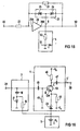
- FIG. 15 shows an embodiment of a low pass according to FIG. 12, in which the controllable capacitive component 23 comprises two capacitance diodes 24 and 25 connected in series.
- the control means 5 apply a control voltage U C to the two capacitance diodes 24 and 25 via an electrical control line 8, for example, in the reverse direction.
- the control means 5 preferably contain a series resistor 52 and a control voltage source 51, which provides the control voltage U C.
- the control voltage U C is preferably selected such that neither of the two capacitance diodes 24 or 25 becomes conductive over the intended modulation range of the amplifier 20.
- Control means 5 one for both transmission elements 3 and 4 in common provided control voltage source included with the controllable capacitive components of both transmission elements 3 and 4 is connected.
- the 16 shows an embodiment of an amplifier device 2 with the two transmission elements 3 and 4 common control means 5.
- the first transmission element 3 contains a resistor 16, a pin diode 17 and a capacitor 18.
- the second transmission element 4 contains at least one bipolar transistor 19 as Amplifier and a negative feedback circuit for this at least one amplifier, which contains at least one capacitance diode as controllable capacitive component 23.
- the base B of the bipolar transistor 19 is preferably connected via a capacitance 49 and via the first transmission element 3 to the input 2A of the amplifier device 2.
- the collector C of the bipolar transistor 19 is connected to the output 2B of the amplifier device 2 via a capacitance 47.
- a positive supply voltage is present at the collector C of the bipolar transistor 19 via a series resistor 46.
- Emitter EM of the bipolar transistor 19 is a negative emitter voltage -U e via a series resistor 48.
- the signs of the two fixed voltages + U 0 and -U e apply to an npn transistor 19 and are of course interchangeable for a pnp transistor.
- a capacitance diode as controllable capacitive component 23 is now connected between the emitter EM of the bipolar transistor 19 and a control voltage source as the control means 5.
- the control means 5 apply a control voltage U C to the capacitance diode 23 operated in the reverse direction to control the capacitance of the capacitance diode 23.
- the frequency response of the transmission element 4 is a pre-emphasis element. Its thus positive edge can be shifted by changing the control voltage U C.
- Another capacitor 45 is connected to zero potential between the capacitor 49 and the bipolar transistor 19 in order to fix the base potential at the base B of the transistor 19.
- the control means 5 are also connected to the first transmission element 3.
- the control voltage U C is applied to a circuit point between the pin diode 17 and the capacitor 18 via the resistor 16.
- the series circuit of capacitance 18 and pin diode 17 is connected between the input 2A of the amplifier device 2 and zero potential.
- the first transmission element 3 forms, together with the internal resistance of the converter element 1, a low-pass filter with regard to its frequency response.
- the resistance of the pin diode 17 can be controlled by the control voltage U C of the control means 5.
- the resistance of the pin diode 17 also changes the cutoff frequency of the low pass formed with the first transmission element 3. By controlling the control voltage U C , the negative edge of the first transmission element 3 can therefore be shifted in addition to the positive edge of the second transmission element 4.
- amplifier devices have 2 in the embodiment according to FIG. 16 for arrays of converter elements 1 required good synchronization properties.
- the pin diode 17 is indeed in the forward direction operated, but are to control their resistance because of the comparatively high internal resistance of the converter element 1 only relatively low currents, typically less than 80 ⁇ A required.
- the associated maximum power loss is typically only a few 100 ⁇ W. Because of Transmission element 3 with the pin diode 17, the received signals S are weakened, is sufficient for the negative feedback bipolar Transistor 19 already has a low quiescent current not more than 100 ⁇ A. The power loss of the entire Amplifier device 2 is therefore very small.
- a gain variation according to FIG. 8 can be realized with the embodiment shown in FIG.
- the minimum gain A min and thus the modulation and dynamics of the amplifier device 2 can be determined by setting the maximum control voltage U C to be applied.
- bipolar transistor 19 instead of only one bipolar transistor 19 as an amplifier can also be a broadband cascode circuit of several bipolar transistors can be provided.
- the amplifier device 2 can in a not shown Embodiment also only one between input 2A and output 2B switched transmission element 3 or 4 in one of the above Embodiments with the at least one capacitive component 23 included.
- the amplifier device 2 is indeed on compensation the frequency response of the capacitive control of the gain A * or A omitted in the converter head 9, but can this frequency response also from a downstream signal processing Getting corrected.
- the amplifier device 2 in particular bipolar Transistors, field effect transistors, in particular MOSFETs, or also integrated operational amplifiers can be used. These three types of amplifiers are particularly suitable for Integration with an array of converter elements 1 in the converter head 9th
Landscapes
- Engineering & Computer Science (AREA)
- Mechanical Engineering (AREA)
- Ultra Sonic Daignosis Equipment (AREA)
- Amplifiers (AREA)
- Measurement Of Velocity Or Position Using Acoustic Or Ultrasonic Waves (AREA)
- Investigating Or Analyzing Materials By The Use Of Ultrasonic Waves (AREA)
Claims (13)
- Tête (9) de transducteur à ultrason comprenanta) au moins un élément (1) transducteur qui reçoit des signaux d'ultrason et les transforme en signaux (S) électriques de réception et comprenant(b) un dispositif (2) amplificateur qui amplifie électriquement les signaux (S) de réception de l'élément (1) transducteur
caractérisée en ce quec) le dispositif (2) amplificateur comporte au moins un composant (23, 24, 25) capacitif qui peut être commandé et le gain (A*, A) du dispositif (2) amplificateur peut être commandé en fonction de la capacité du composant (23, 24, 25) capacitif. - Tête de transducteur à ultrason suivant la revendication 1, dans laquelle le dispositif (2) amplificateura) comprend au moins un amplificateur (6, 19, 20) etb) un circuit à contre-réaction avec le composant (23) capacitif qui peut être commandé pour ce au moins un amplificateur (6, 19, 20).
- Tête de transducteur à ultrason suivant la revendication 2, dans laquelle il est prévu comme amplificateur un transistor (6) à effet de champ dont la grille (CG) est reliée électriquement à l'élément (1) transducteur et dont la source (SC) est reliée à le au moins un composant (23) capacitif.
- Tête de transducteur à ultrason suivant la revendication 2, dans laquelle il est prévu comme amplificateur un transistor (19) bipolaire dont la base (B) est reliée à l'élément (1) transducteur et dont l'émetteur (EM) est relié à le au moins un composant (23) capacitif.
- Tête de transducteur à ultrason suivant l'une des revendications précédentes, dans laquellea) le dispositif (2) amplificateur comprend deux éléments (3, 4) de transfert montés électriquement en série entre une entrée (2A) pour le signal (S) de réception et une sortie (2B) pour le signal (S') amplifié de réception, éléments qui ont respectivement une fonction (G,H) de transfert logarithmique en fonction de la fréquence ayant un front (E, F) dépendant de manière sensiblement linéaire d'une fonction (V(f)) bijective de la fréquence (f), les pentes des deux fronts (E, F) des deux fonctions ( G, H) de transfert étant sensiblement les mêmes en valeur absolue et ayant des signes différentsb) au moins l'un des deux éléments (3, 4) de transfert comportant le au moins un composant (3) capacitif qui peut être commandéc) et dans laquelled) les fronts (E, F) des fonctions ( G, H) de transfert des deux éléments (3, 4) de transfert peuvent être déplacés l'un par rapport à l'autre dans un domaine (Δf) de fréquence du signal (S) de réception.
- Tête de transducteur à ultrason suivant la revendication 5, dans laquelle l'élément (4) de transfert, dont la fonction ( H) de transfert a le front (F) ayant la pente positive, comporte un filtre passe-haut au moins du premier ordre, un différentiateur et/ou un organe de pré-accentuation.
- Tête de transducteur à ultrason suivant la revendication 5 ou la revendication 6, dans laquelle l'élément (3) de transfert, dont la fonction ( G) de transfert a le front (E) ayant la pente négative, comprend un passe-bas au moins du premier ordre, un intégrateur et/ou un élément de désaccentuation.
- Tête de transducteur à ultrason suivant l'une des revendications 5 à 7, dans laquelle chacun des deux éléments (3, 4) de transfert du dispositif (2) amplificateur a au moins un composant (23, 26) capacitif qui peut être commandé.
- Tête de transducteur à ultrason suivant l'une des revendications 2 à 4 et l'une des revendications 5 à 8, dans laquelle l'un des deux éléments (4) de transfert comprend le au moins un amplificateur (6, 19, 20) à contre-réaction et l'autre élément (3) de transfert comprend une diode (17) de type pin qui peut être commandée.
- Tête de transducteur à ultrason suivant l'une des revendications précédentes dans laquelle le au moins un composant capacitif est une diode (23, 24, 25) à capacité.
- Tête de transducteur à ultrason suivant l'une des revendications précédentes, comprenant un réseau bidimensionnel d'éléments (1) transducteurs et un dispositif (2) amplificateur pour chacun de ces éléments (1) transducteurs.
- Appareil à ultrason comprenant une tête (9) de transducteur d'ultrason selon l'une des revendications précédentes et des moyens (5) de commande destinés à commander la capacité (C) du au moins un composant (23) capacitif de chaque dispositif (2) amplificateur.
- Appareil à ultrason suivant la revendication 12, dans lequela) il est prévu des moyens (31) de traitement du signal pour la constitution d'une image de l'objet à partir des signaux (S') de réception du au moins un élément transducteur, qui ont été amplifiés par le dispositif (2) amplificateurb) ces moyens (31) de traitement du signal sont reliés aux sorties (2B) des dispositifs (2) amplificateurs de la tête (9) de transducteur à ultrason par des conducteurs (34) de signaux etc) les impédances de sortie des dispositifs (2) amplificateurs sont adaptés au moins approximativement aux impédances des conducteurs (34) de signalisation associés.
Applications Claiming Priority (2)
| Application Number | Priority Date | Filing Date | Title |
|---|---|---|---|
| DE19514308A DE19514308A1 (de) | 1995-04-18 | 1995-04-18 | Ultraschallwandlerkopf mit integrierten steuerbaren Verstärkereinrichtungen |
| DE19514308 | 1995-04-18 |
Publications (3)
| Publication Number | Publication Date |
|---|---|
| EP0738883A2 EP0738883A2 (fr) | 1996-10-23 |
| EP0738883A3 EP0738883A3 (fr) | 1997-04-02 |
| EP0738883B1 true EP0738883B1 (fr) | 2002-11-27 |
Family
ID=7759828
Family Applications (1)
| Application Number | Title | Priority Date | Filing Date |
|---|---|---|---|
| EP96105227A Expired - Lifetime EP0738883B1 (fr) | 1995-04-18 | 1996-04-01 | Transducteur à ultrason intégré avec un amplificateur réglable |
Country Status (5)
| Country | Link |
|---|---|
| US (1) | US5724312A (fr) |
| EP (1) | EP0738883B1 (fr) |
| DE (2) | DE19514308A1 (fr) |
| DK (1) | DK0738883T3 (fr) |
| ES (1) | ES2186744T3 (fr) |
Families Citing this family (13)
| Publication number | Priority date | Publication date | Assignee | Title |
|---|---|---|---|---|
| DE19841220C1 (de) * | 1998-09-09 | 2000-05-04 | Siemens Ag | Ultraschallgerät |
| US6621341B1 (en) | 2000-05-22 | 2003-09-16 | Acuson Corporation | Diagnostic medical ultrasound systems having a method and circuitry for front-end gain control |
| US20030002682A1 (en) * | 2001-07-02 | 2003-01-02 | Phonex Broadband Corporation | Wireless audio/mechanical vibration transducer and audio/visual transducer |
| ES2402270T3 (es) * | 2002-10-10 | 2013-04-30 | Visualsonics Inc. | Sistema de formación de imágenes por ultrasonidos de alta frecuencia y de alta frecuencia de fotogramas |
| JP2007525299A (ja) * | 2004-03-01 | 2007-09-06 | サニーブルック アンド ウィメンズ カレッジ ヘルス サイエンシーズ センター | Ecgトリガレトロスペクティブカラーフロー超音波イメージングのためのシステムおよび方法 |
| JP4805254B2 (ja) | 2004-04-20 | 2011-11-02 | ビジュアルソニックス インコーポレイテッド | 配列された超音波トランスデューサ |
| US7901358B2 (en) * | 2005-11-02 | 2011-03-08 | Visualsonics Inc. | High frequency array ultrasound system |
| US7570112B2 (en) * | 2005-12-15 | 2009-08-04 | Siemens Medical Solutions Usa, Inc. | Ultrasound imaging or other use variable input impedance preamplifier |
| CN104470729B (zh) | 2012-07-18 | 2018-02-06 | 皇家飞利浦有限公司 | 用于驱动负载,尤其是驱动超声换能器的驱动器设备和驱动方法 |
| JP6321980B2 (ja) * | 2013-03-09 | 2018-05-09 | キヤノン株式会社 | 検出回路、駆動方法、プローブ、及び被検体情報取得装置 |
| FR3059494A1 (fr) * | 2016-11-29 | 2018-06-01 | Universite D'aix-Marseille | Circuit amplificateur de charges a gain de conversion eleve |
| RU199936U1 (ru) * | 2020-06-05 | 2020-09-29 | Публичное Акционерное Общество "Одк-Сатурн" | Устройство для измерения вибрации |
| CN121253688B (zh) * | 2025-12-01 | 2026-03-10 | 中北大学 | 具有一激多收功能的非接触式超声导波检测仪器 |
Family Cites Families (17)
| Publication number | Priority date | Publication date | Assignee | Title |
|---|---|---|---|---|
| DE48278C (de) * | 1970-07-17 | E. CA-REZ in Brüssel, Nr. 72 Rue du Marais | Neuerung bei dem Verfahren zur Darstellung von Ammoniumnitrat durch Umsetzen von Bariumnitrat mit Ammoniumsulfat | |
| US3851301A (en) * | 1972-09-15 | 1974-11-26 | Kidde & Co Walter | Method and apparatus for balancing an ultrasonic detection system |
| US4140107A (en) * | 1972-12-28 | 1979-02-20 | Erasmus University Rotterdam | Echoscope for examination of objects |
| US3975704A (en) * | 1974-11-04 | 1976-08-17 | Klein Associates, Inc. | Method of and apparatus for sonar and related signal texture enhancement of recording media |
| JPS53142075A (en) * | 1977-05-17 | 1978-12-11 | Tokyo Shibaura Electric Co | Ultrasonic diagnosing device |
| JPS5492307A (en) * | 1977-12-29 | 1979-07-21 | Sony Corp | Driving circuit of electrostrictive converter |
| DE2942641A1 (de) * | 1979-10-22 | 1981-04-30 | Deutsche Itt Industries Gmbh, 7800 Freiburg | Telefon-sprechkapsel-innenschaltung als kohlemikrophonersatz |
| GB2114296B (en) * | 1982-01-29 | 1985-08-29 | Emi Ltd | A ultrasonic transducer array |
| JPS58152546A (ja) * | 1982-03-04 | 1983-09-10 | 横河電機株式会社 | 超音波診断装置の反射波受信方式 |
| US4489729A (en) * | 1982-09-03 | 1984-12-25 | Medtronic, Inc. | Ultrasound imaging system |
| JPS60158840A (ja) * | 1984-01-31 | 1985-08-20 | 株式会社東芝 | 超音波診断装置 |
| FR2593919A1 (fr) * | 1986-02-04 | 1987-08-07 | Labo Electronique Physique | Appareil d'examen de milieux par echographie ultrasonore |
| JPH0696009B2 (ja) * | 1986-09-30 | 1994-11-30 | 株式会社東芝 | 超音波診断装置 |
| FR2614152B1 (fr) * | 1987-04-14 | 1991-06-14 | Thomson Csf | Procede de compensation d'un circuit a amplificateur de charge notamment pour hydrophone piezoelectrique |
| JP2735203B2 (ja) * | 1987-12-17 | 1998-04-02 | 株式会社東芝 | 超音波診断装置 |
| EP0600654A1 (fr) * | 1992-12-04 | 1994-06-08 | Hewlett-Packard Company | Capteur ultrasonique avec un amplificateur à gain variable intégré |
| DE4318531C2 (de) * | 1993-06-03 | 1995-08-31 | Hirschmann Richard Gmbh Co | Verfahren und Schaltungsanordnung zum Verstärken von in einem breiten Frequenzbereich liegenden Signalen |
-
1995
- 1995-04-18 DE DE19514308A patent/DE19514308A1/de not_active Withdrawn
-
1996
- 1996-04-01 ES ES96105227T patent/ES2186744T3/es not_active Expired - Lifetime
- 1996-04-01 DE DE59609897T patent/DE59609897D1/de not_active Expired - Lifetime
- 1996-04-01 DK DK96105227T patent/DK0738883T3/da active
- 1996-04-01 EP EP96105227A patent/EP0738883B1/fr not_active Expired - Lifetime
- 1996-04-17 US US08/632,815 patent/US5724312A/en not_active Expired - Lifetime
Also Published As
| Publication number | Publication date |
|---|---|
| EP0738883A3 (fr) | 1997-04-02 |
| ES2186744T3 (es) | 2003-05-16 |
| US5724312A (en) | 1998-03-03 |
| DE19514308A1 (de) | 1996-10-24 |
| DE59609897D1 (de) | 2003-01-09 |
| DK0738883T3 (da) | 2003-03-17 |
| EP0738883A2 (fr) | 1996-10-23 |
Similar Documents
| Publication | Publication Date | Title |
|---|---|---|
| EP0738883B1 (fr) | Transducteur à ultrason intégré avec un amplificateur réglable | |
| DE69131230T2 (de) | Lineare verstärkungsregelung eines verstärkers | |
| DE2713953C3 (de) | Oberwellengenerator zur Erzeugung der dritten Harmonischen | |
| DE69505649T2 (de) | Verstärkerschaltung | |
| DE19815878B4 (de) | Ausgangstreiberschaltung und Verfahren zur Signalübertragung zwischen integrierten Halbleiterschaltungen unter Verwendung derselben | |
| DE10129850B4 (de) | Verstärkereinrichtung mit frequenzgangkompensierender Verstärkerreaktanz sowie Verwendung der Verstärkereinrichtung | |
| DE2718491C2 (de) | Schaltungsanordnung zur Verstärkung der Signale eines elektromagnetischen Wandlers und zur Vorspannungserzeugung für den Wandler | |
| DE2123826C3 (de) | Vorrichtung zur Verbesserung des Signal/Rausch-Verhältnisses einer Empfängeranordnung mit zwei Empfangsantennen | |
| DE19836997B4 (de) | Sende/Empfangs-Schaltkreis und Sende/Empfangs-Verfahren für einen Wandler | |
| DE69611749T2 (de) | Verstärkerschaltung mit variabler Verstärkung | |
| DE2950584A1 (de) | Schaltungsanordnung mit steuerbarem widerstand | |
| DE2535695A1 (de) | Verstaerker mit variabler verstaerkung | |
| DE69327013T2 (de) | Stromversorgungsvorrichtung für Mikrofon | |
| DE3212451C2 (de) | Schaltungsanordnung zum Erzeugen eines auf einen Pegel eines Eingangssignals bezogenen Ausgangssignals | |
| DE3147171C2 (fr) | ||
| EP2856642B1 (fr) | Amplificateur commuté destiné à une tension d'alimentation variable | |
| DE19946459B4 (de) | Rauscharme breitbandige Verstärkereinrichtung sowie Verwendung der Verstärkereinrichtung | |
| DE2502009A1 (de) | Frequenzgang-entzerrer fuer elektromechanische wandler | |
| DE3724980A1 (de) | Spannungswiederholerschaltung fuer eine ohmsche komponente aufweisende last mit kompensation der oberwellenverzerrung | |
| DE4304013C2 (de) | Anordnung zur Übertragung von Signalwechselspannungen, insbesondere Tonsignalen über eine Leitung | |
| EP0811272A1 (fr) | Dispositif d'amplification reglable servant a amplifier des signaux electriques dans une place predeterminee de frequences | |
| DE3029439C2 (fr) | ||
| WO2005112298A1 (fr) | Regulation de puissance dans des emetteurs haute frequence | |
| EP0590516B1 (fr) | Dispositif commandé en tension | |
| DE69300194T2 (de) | Steuerungsschaltkreis für einen amplitudenmodulierten Halbleiterlaser. |
Legal Events
| Date | Code | Title | Description |
|---|---|---|---|
| PUAI | Public reference made under article 153(3) epc to a published international application that has entered the european phase |
Free format text: ORIGINAL CODE: 0009012 |
|
| AK | Designated contracting states |
Kind code of ref document: A2 Designated state(s): DE DK ES FR |
|
| PUAL | Search report despatched |
Free format text: ORIGINAL CODE: 0009013 |
|
| AK | Designated contracting states |
Kind code of ref document: A3 Designated state(s): DE DK ES FR |
|
| 17P | Request for examination filed |
Effective date: 19970918 |
|
| 17Q | First examination report despatched |
Effective date: 20001027 |
|
| GRAG | Despatch of communication of intention to grant |
Free format text: ORIGINAL CODE: EPIDOS AGRA |
|
| GRAG | Despatch of communication of intention to grant |
Free format text: ORIGINAL CODE: EPIDOS AGRA |
|
| GRAH | Despatch of communication of intention to grant a patent |
Free format text: ORIGINAL CODE: EPIDOS IGRA |
|
| GRAH | Despatch of communication of intention to grant a patent |
Free format text: ORIGINAL CODE: EPIDOS IGRA |
|
| GRAH | Despatch of communication of intention to grant a patent |
Free format text: ORIGINAL CODE: EPIDOS IGRA |
|
| GRAH | Despatch of communication of intention to grant a patent |
Free format text: ORIGINAL CODE: EPIDOS IGRA |
|
| GRAA | (expected) grant |
Free format text: ORIGINAL CODE: 0009210 |
|
| RAP1 | Party data changed (applicant data changed or rights of an application transferred) |
Owner name: INTELLIGENDT SYSTEMS & SERVICES GMBH & CO. KG |
|
| AK | Designated contracting states |
Kind code of ref document: B1 Designated state(s): DE DK ES FR |
|
| REF | Corresponds to: |
Ref document number: 59609897 Country of ref document: DE Date of ref document: 20030109 |
|
| REG | Reference to a national code |
Ref country code: DK Ref legal event code: T3 |
|
| REG | Reference to a national code |
Ref country code: ES Ref legal event code: FG2A Ref document number: 2186744 Country of ref document: ES Kind code of ref document: T3 |
|
| ET | Fr: translation filed | ||
| PLBE | No opposition filed within time limit |
Free format text: ORIGINAL CODE: 0009261 |
|
| STAA | Information on the status of an ep patent application or granted ep patent |
Free format text: STATUS: NO OPPOSITION FILED WITHIN TIME LIMIT |
|
| 26N | No opposition filed |
Effective date: 20030828 |
|
| REG | Reference to a national code |
Ref country code: FR Ref legal event code: TP Ref country code: FR Ref legal event code: CD |
|
| REG | Reference to a national code |
Ref country code: ES Ref legal event code: PC2A Owner name: "INTELLIGENDT SYSTEMS & Effective date: 20110503 Ref country code: ES Ref legal event code: PC2A Owner name: INTELLIGENDT SYSTEMS & SERVICES GMBH Effective date: 20110503 |
|
| PGFP | Annual fee paid to national office [announced via postgrant information from national office to epo] |
Ref country code: ES Payment date: 20110419 Year of fee payment: 16 |
|
| PGFP | Annual fee paid to national office [announced via postgrant information from national office to epo] |
Ref country code: DK Payment date: 20110426 Year of fee payment: 16 |
|
| PGFP | Annual fee paid to national office [announced via postgrant information from national office to epo] |
Ref country code: DE Payment date: 20110620 Year of fee payment: 16 |
|
| PGFP | Annual fee paid to national office [announced via postgrant information from national office to epo] |
Ref country code: FR Payment date: 20120511 Year of fee payment: 17 |
|
| REG | Reference to a national code |
Ref country code: DK Ref legal event code: EBP |
|
| REG | Reference to a national code |
Ref country code: DE Ref legal event code: R119 Ref document number: 59609897 Country of ref document: DE Effective date: 20121101 |
|
| REG | Reference to a national code |
Ref country code: ES Ref legal event code: FD2A Effective date: 20130715 |
|
| PG25 | Lapsed in a contracting state [announced via postgrant information from national office to epo] |
Ref country code: ES Free format text: LAPSE BECAUSE OF NON-PAYMENT OF DUE FEES Effective date: 20120402 |
|
| PG25 | Lapsed in a contracting state [announced via postgrant information from national office to epo] |
Ref country code: DK Free format text: LAPSE BECAUSE OF NON-PAYMENT OF DUE FEES Effective date: 20120430 |
|
| REG | Reference to a national code |
Ref country code: FR Ref legal event code: ST Effective date: 20131231 |
|
| PG25 | Lapsed in a contracting state [announced via postgrant information from national office to epo] |
Ref country code: FR Free format text: LAPSE BECAUSE OF NON-PAYMENT OF DUE FEES Effective date: 20130430 |
|
| PG25 | Lapsed in a contracting state [announced via postgrant information from national office to epo] |
Ref country code: DE Free format text: LAPSE BECAUSE OF NON-PAYMENT OF DUE FEES Effective date: 20121101 |