EP0738974A2 - Dispositif de mémoire à accès sériel avec tolérance de fautes améliorée - Google Patents
Dispositif de mémoire à accès sériel avec tolérance de fautes améliorée Download PDFInfo
- Publication number
- EP0738974A2 EP0738974A2 EP96104260A EP96104260A EP0738974A2 EP 0738974 A2 EP0738974 A2 EP 0738974A2 EP 96104260 A EP96104260 A EP 96104260A EP 96104260 A EP96104260 A EP 96104260A EP 0738974 A2 EP0738974 A2 EP 0738974A2
- Authority
- EP
- European Patent Office
- Prior art keywords
- column
- row
- clock signal
- line
- selection device
- Prior art date
- Legal status (The legal status is an assumption and is not a legal conclusion. Google has not performed a legal analysis and makes no representation as to the accuracy of the status listed.)
- Granted
Links
Images
Classifications
-
- G—PHYSICS
- G11—INFORMATION STORAGE
- G11C—STATIC STORES
- G11C11/00—Digital stores characterised by the use of particular electric or magnetic storage elements; Storage elements therefor
- G11C11/21—Digital stores characterised by the use of particular electric or magnetic storage elements; Storage elements therefor using electric elements
- G11C11/34—Digital stores characterised by the use of particular electric or magnetic storage elements; Storage elements therefor using electric elements using semiconductor devices
- G11C11/40—Digital stores characterised by the use of particular electric or magnetic storage elements; Storage elements therefor using electric elements using semiconductor devices using transistors
-
- G—PHYSICS
- G11—INFORMATION STORAGE
- G11C—STATIC STORES
- G11C29/00—Checking stores for correct operation ; Subsequent repair; Testing stores during standby or offline operation
- G11C29/70—Masking faults in memories by using spares or by reconfiguring
- G11C29/86—Masking faults in memories by using spares or by reconfiguring in serial access memories, e.g. shift registers, CCDs, bubble memories
-
- G—PHYSICS
- G06—COMPUTING OR CALCULATING; COUNTING
- G06F—ELECTRIC DIGITAL DATA PROCESSING
- G06F11/00—Error detection; Error correction; Monitoring
- G06F11/07—Responding to the occurrence of a fault, e.g. fault tolerance
- G06F11/08—Error detection or correction by redundancy in data representation, e.g. by using checking codes
- G06F11/10—Adding special bits or symbols to the coded information, e.g. parity check, casting out 9's or 11's
- G06F11/1008—Adding special bits or symbols to the coded information, e.g. parity check, casting out 9's or 11's in individual solid state devices
-
- G—PHYSICS
- G11—INFORMATION STORAGE
- G11C—STATIC STORES
- G11C29/00—Checking stores for correct operation ; Subsequent repair; Testing stores during standby or offline operation
- G11C29/70—Masking faults in memories by using spares or by reconfiguring
- G11C29/88—Masking faults in memories by using spares or by reconfiguring with partially good memories
Definitions
- a memory device with serial access is known with a memory matrix, the memory cells of which are arranged in M rows and N columns and connected to row lines and column lines, with a column selection device which is connected to the column lines and to each Cyclically advancing a clock signal by one column, and with a row selection device which is connected to the row lines and proceeds with a clock signal by one row in the row selection.
- the number of shift register stages in the column selection device is reduced by a gate circuit in the column selection device.
- Claims 2 and 5 relate to advantageous embodiments of the invention.
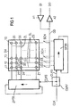
- FIG. 1 shows a memory device with serial access according to the invention, which has a memory matrix SM, the memory cells 11... ZS of which are arranged in Z rows and S columns and whose memory cells are each connected to row lines ZL and column lines SL.
- the memory device according to the invention has a line selection device ZPTR, which is driven by a line clock signal CLKZ and whose outputs are connected to the line lines.
- a signal feedback is indicated in the line selection device ZPTR, which indicates a cyclical selection of the line lines ZL.
- the memory device has a column selection device which consists of switches SCH and a column addressing unit SPTR, wherein for a switch is provided for each column of the memory matrix SM and each switch is connected to a respective output of the column addressing unit SPTR.
- the column addressing unit SPTR is controlled by column clock signal CLKS and a drawn-in signal feedback indicates a cyclical addressing.
- the switches SCH have the task of connecting an addressed column line to a common data line GD.
- External input data DI are amplified by an existing input amplifier A1 and connected to the common data line GD, and output data present on the common data line are amplified by an output amplifier A2 before they are available as external output data DO.
- the row clock signal CLKZ and the column clock signal CLKS are formed in a column logic circuit CLKV from an external clock signal CLK.
- the column logic circuit CLKV consists, for example, of two frequency divider circuits based on flip-flops. In the simplest case, both the row clock signal and the column clock signal are the same as the external clock signal CLK and the circuit CLKV consists only of connections to the external one, as indicated by the broken line in FIG Clock signal.
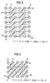
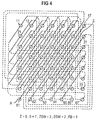
- FB 2 consecutive columns
- the order of access within the physical limits of the cell array of the memory matrix SM is by means of solid lines and the transitions over the physical limits of the cell field are indicated by dashed lines.
- the first block to be read out here consists of cells 71, 72, 63, 64, 55, 56, 41, 42, 33, 34, 25, 26, 11, 12.
- FB 1 consecutive columns
- there is also a row change with a transition from the fifth column back to the first column.
- the order of access within the physical boundaries of the cell array of the memory matrix SM is indicated by solid lines and the transitions beyond the physical boundaries of the cell array are indicated by dashed lines.
- the first block to be read out here consists of cells 41, 32, 23, 14.
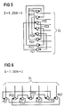
- the faulty cells are often not only concentrated in one row and / or column, but also neighboring rows and / or neighboring columns are affected in the event of an error, it may be advantageous to use the interlaced width and / or to choose the column jump width different from one.
- FIG. 4 shows an example of a memory matrix with the memory cells 11... 87 with eight rows and seven columns, the cell 81 being the starting cell A and thus the cell 36 representing the end cell E, and the memory cells being the same as in a conventional matrix indexing are named.
- the line jump ZSW is three and the column jump SSW is two.
- the memory cells are connected to one another by a graph starting with A and ending with E in the order of access, the transitions over the edge of the physical edge being represented by dashed lines and all other transitions being represented by solid lines.
- the memory cells are addressed in the order given below.
- a corresponding column addressing unit SPTR is shown in FIG. 6, which controls the switches SCH for the respective column lines.
- the outputs of the register stages PS1 ... PS7 are assigned in turn to the column lines SL for the columns 1 ... 7.
- the entire storage device can also be rotated through 90 °, which means that the rows and columns as well as the line jump width and the column jump width are interchanged.
Landscapes
- Engineering & Computer Science (AREA)
- Theoretical Computer Science (AREA)
- Quality & Reliability (AREA)
- Physics & Mathematics (AREA)
- General Engineering & Computer Science (AREA)
- General Physics & Mathematics (AREA)
- Microelectronics & Electronic Packaging (AREA)
- Computer Hardware Design (AREA)
- For Increasing The Reliability Of Semiconductor Memories (AREA)
- Detection And Correction Of Errors (AREA)
- Techniques For Improving Reliability Of Storages (AREA)
- Debugging And Monitoring (AREA)
- Dram (AREA)
Applications Claiming Priority (2)
| Application Number | Priority Date | Filing Date | Title |
|---|---|---|---|
| DE19512791 | 1995-04-05 | ||
| DE19512791 | 1995-04-05 |
Publications (3)
| Publication Number | Publication Date |
|---|---|
| EP0738974A2 true EP0738974A2 (fr) | 1996-10-23 |
| EP0738974A3 EP0738974A3 (fr) | 1999-06-02 |
| EP0738974B1 EP0738974B1 (fr) | 2002-05-22 |
Family
ID=7758876
Family Applications (1)
| Application Number | Title | Priority Date | Filing Date |
|---|---|---|---|
| EP96104260A Expired - Lifetime EP0738974B1 (fr) | 1995-04-05 | 1996-03-15 | Dispositif de mémoire à accès sériel avec tolérance de fautes améliorée |
Country Status (7)
| Country | Link |
|---|---|
| US (1) | US5751742A (fr) |
| EP (1) | EP0738974B1 (fr) |
| JP (1) | JP3850484B2 (fr) |
| KR (1) | KR100409113B1 (fr) |
| AT (1) | ATE217987T1 (fr) |
| DE (1) | DE59609221D1 (fr) |
| TW (1) | TW312763B (fr) |
Cited By (2)
| Publication number | Priority date | Publication date | Assignee | Title |
|---|---|---|---|---|
| US6097661A (en) * | 1997-09-26 | 2000-08-01 | Siemens Aktiengesellschaft | Pointer circuit with low surface requirement high speed and low power loss |
| US6138227A (en) * | 1995-09-13 | 2000-10-24 | Siemens Aktiengesellschaft | Device for the jump-like addressing of specific lines of a serially operating digital memory |
Families Citing this family (1)
| Publication number | Priority date | Publication date | Assignee | Title |
|---|---|---|---|---|
| ATE430365T1 (de) * | 2003-05-22 | 2009-05-15 | Nxp Bv | Test von ram addressdekodierern auf widerstandsbehaftete leiterunterbrechungen |
Family Cites Families (5)
| Publication number | Priority date | Publication date | Assignee | Title |
|---|---|---|---|---|
| US3812336A (en) * | 1972-12-18 | 1974-05-21 | Ibm | Dynamic address translation scheme using orthogonal squares |
| JPS58139399A (ja) * | 1982-02-15 | 1983-08-18 | Hitachi Ltd | 半導体記憶装置 |
| EP0189699B1 (fr) * | 1984-12-26 | 1992-09-30 | STMicroelectronics, Inc. | Mémoire morte à lignes de bit interdigitales |
| US4903242A (en) * | 1987-05-06 | 1990-02-20 | Nec Corporation | Serial access memory circuit with improved serial addressing circuit composed of a shift register |
| JP2816512B2 (ja) * | 1992-07-27 | 1998-10-27 | 三菱電機株式会社 | 半導体記憶装置 |
-
1996
- 1996-02-29 TW TW085102428A patent/TW312763B/zh active
- 1996-03-15 DE DE59609221T patent/DE59609221D1/de not_active Expired - Fee Related
- 1996-03-15 EP EP96104260A patent/EP0738974B1/fr not_active Expired - Lifetime
- 1996-03-15 AT AT96104260T patent/ATE217987T1/de not_active IP Right Cessation
- 1996-04-02 US US08/626,512 patent/US5751742A/en not_active Expired - Lifetime
- 1996-04-04 KR KR1019960010103A patent/KR100409113B1/ko not_active Expired - Fee Related
- 1996-04-05 JP JP08413396A patent/JP3850484B2/ja not_active Expired - Fee Related
Cited By (2)
| Publication number | Priority date | Publication date | Assignee | Title |
|---|---|---|---|---|
| US6138227A (en) * | 1995-09-13 | 2000-10-24 | Siemens Aktiengesellschaft | Device for the jump-like addressing of specific lines of a serially operating digital memory |
| US6097661A (en) * | 1997-09-26 | 2000-08-01 | Siemens Aktiengesellschaft | Pointer circuit with low surface requirement high speed and low power loss |
Also Published As
| Publication number | Publication date |
|---|---|
| JPH08287699A (ja) | 1996-11-01 |
| ATE217987T1 (de) | 2002-06-15 |
| US5751742A (en) | 1998-05-12 |
| EP0738974B1 (fr) | 2002-05-22 |
| JP3850484B2 (ja) | 2006-11-29 |
| KR100409113B1 (ko) | 2004-03-18 |
| KR960038976A (ko) | 1996-11-21 |
| EP0738974A3 (fr) | 1999-06-02 |
| TW312763B (fr) | 1997-08-11 |
| DE59609221D1 (de) | 2002-06-27 |
Similar Documents
| Publication | Publication Date | Title |
|---|---|---|
| DE2646162C3 (de) | Schaltungsanordnung zum Ersetzen fehlerhafter Informationen in Speicherplätzen eines nicht veränderbaren Speichers | |
| DE3886114T2 (de) | Halbleiterspeichergerät mit redundanter Speicherzellenmatrix. | |
| DE2646163C3 (de) | Schaltungsanordnung zum Ersetzen fehlerhafter Informationen in Speicherplätzen eines nicht veränderbaren Speichers | |
| EP0850481B1 (fr) | Dispositif permettant d'adresser par saut des lignes determinees d'une memoire numerique a fonctionnement sequentiel | |
| DE2328869C2 (de) | Verfahren und Schaltungsanordnung zum Betreiben eines digitalen Speichersystems | |
| DE68925090T2 (de) | Speicherschaltung mit verbesserter Redundanzstruktur | |
| DE3209679C2 (fr) | ||
| DE2132565A1 (de) | Umsetzer | |
| DE69020384T2 (de) | Integrierte Halbleiterspeicherschaltung mit Möglichkeit zum Maskieren des Schreibens im Speicher. | |
| DE3412677C2 (fr) | ||
| DE3015992A1 (de) | Programmierbare logische anordnung | |
| DE1549468A1 (de) | Speicheranordnung fuer ein programmgesteuertes Datenverarbeitungssystem | |
| DE2400064A1 (de) | Speicherpruefanordnung und diese verwendendes endgeraetsystem in einem datenverarbeitungssystem | |
| DE3121742A1 (de) | Mikroprogrammsteuerverfahren und -einrichtung zu dessen durchfuehrung | |
| DE3903486C2 (fr) | ||
| DE3333366A1 (de) | Aufloesungsnetzwerk fuer zuletzt erfolgte benutzungen | |
| DE4129133C1 (fr) | ||
| DE102007011801B4 (de) | Schaltung zum Erzeugen eines Fehlercodierungsdatenblocks, Vorrichtung mit der Schaltung, Vorrichtung zum Erzeugen eines Fehlercodierungsdatenblocks | |
| EP0738974B1 (fr) | Dispositif de mémoire à accès sériel avec tolérance de fautes améliorée | |
| DE69227144T2 (de) | Programmierbare logische Einheit | |
| DE1234054B (de) | Byte-Umsetzer | |
| DE2629893A1 (de) | Zellenadressierbare matrix | |
| EP0965083B1 (fr) | Memoire de donnees a circuit redondant | |
| DE69026363T2 (de) | Multipositionsverschieber mit Paritätsbitgenerator | |
| DE2242279B2 (de) | Schaltungsanordnung zur Ermittlung von Fehlern in einer Speichereinheit eines programmgesteuerten Datenvermittiungssystems |
Legal Events
| Date | Code | Title | Description |
|---|---|---|---|
| PUAI | Public reference made under article 153(3) epc to a published international application that has entered the european phase |
Free format text: ORIGINAL CODE: 0009012 |
|
| AK | Designated contracting states |
Kind code of ref document: A2 Designated state(s): AT DE FR GB IE IT NL |
|
| PUAL | Search report despatched |
Free format text: ORIGINAL CODE: 0009013 |
|
| AK | Designated contracting states |
Kind code of ref document: A3 Designated state(s): AT DE FR GB IE IT NL |
|
| RIC1 | Information provided on ipc code assigned before grant |
Free format text: 6G 06F 11/20 A, 6G 06F 11/00 B, 6G 06F 11/10 B |
|
| 17P | Request for examination filed |
Effective date: 19990706 |
|
| 17Q | First examination report despatched |
Effective date: 20010301 |
|
| RAP1 | Party data changed (applicant data changed or rights of an application transferred) |
Owner name: INFINEON TECHNOLOGIES AG |
|
| GRAG | Despatch of communication of intention to grant |
Free format text: ORIGINAL CODE: EPIDOS AGRA |
|
| GRAG | Despatch of communication of intention to grant |
Free format text: ORIGINAL CODE: EPIDOS AGRA |
|
| GRAH | Despatch of communication of intention to grant a patent |
Free format text: ORIGINAL CODE: EPIDOS IGRA |
|
| GRAH | Despatch of communication of intention to grant a patent |
Free format text: ORIGINAL CODE: EPIDOS IGRA |
|
| GRAA | (expected) grant |
Free format text: ORIGINAL CODE: 0009210 |
|
| REF | Corresponds to: |
Ref document number: 217987 Country of ref document: AT Date of ref document: 20020615 Kind code of ref document: T |
|
| REG | Reference to a national code |
Ref country code: GB Ref legal event code: FG4D Free format text: NOT ENGLISH |
|
| REG | Reference to a national code |
Ref country code: IE Ref legal event code: FG4D Free format text: GERMAN |
|
| REF | Corresponds to: |
Ref document number: 59609221 Country of ref document: DE Date of ref document: 20020627 |
|
| GBT | Gb: translation of ep patent filed (gb section 77(6)(a)/1977) |
Effective date: 20020814 |
|
| ET | Fr: translation filed | ||
| PLBE | No opposition filed within time limit |
Free format text: ORIGINAL CODE: 0009261 |
|
| STAA | Information on the status of an ep patent application or granted ep patent |
Free format text: STATUS: NO OPPOSITION FILED WITHIN TIME LIMIT |
|
| 26N | No opposition filed |
Effective date: 20030225 |
|
| REG | Reference to a national code |
Ref country code: HK Ref legal event code: WD Ref document number: 1003951 Country of ref document: HK |
|
| PGFP | Annual fee paid to national office [announced via postgrant information from national office to epo] |
Ref country code: NL Payment date: 20060314 Year of fee payment: 11 |
|
| PGFP | Annual fee paid to national office [announced via postgrant information from national office to epo] |
Ref country code: AT Payment date: 20060315 Year of fee payment: 11 |
|
| PGFP | Annual fee paid to national office [announced via postgrant information from national office to epo] |
Ref country code: GB Payment date: 20070322 Year of fee payment: 12 |
|
| PG25 | Lapsed in a contracting state [announced via postgrant information from national office to epo] |
Ref country code: AT Free format text: LAPSE BECAUSE OF NON-PAYMENT OF DUE FEES Effective date: 20070315 |
|
| NLV4 | Nl: lapsed or anulled due to non-payment of the annual fee |
Effective date: 20071001 |
|
| PG25 | Lapsed in a contracting state [announced via postgrant information from national office to epo] |
Ref country code: NL Free format text: LAPSE BECAUSE OF NON-PAYMENT OF DUE FEES Effective date: 20071001 |
|
| PGFP | Annual fee paid to national office [announced via postgrant information from national office to epo] |
Ref country code: IE Payment date: 20080321 Year of fee payment: 13 |
|
| PGFP | Annual fee paid to national office [announced via postgrant information from national office to epo] |
Ref country code: FR Payment date: 20080314 Year of fee payment: 13 Ref country code: DE Payment date: 20080510 Year of fee payment: 13 |
|
| PGFP | Annual fee paid to national office [announced via postgrant information from national office to epo] |
Ref country code: IT Payment date: 20080328 Year of fee payment: 13 |
|
| GBPC | Gb: european patent ceased through non-payment of renewal fee |
Effective date: 20080315 |
|
| PG25 | Lapsed in a contracting state [announced via postgrant information from national office to epo] |
Ref country code: GB Free format text: LAPSE BECAUSE OF NON-PAYMENT OF DUE FEES Effective date: 20080315 |
|
| REG | Reference to a national code |
Ref country code: FR Ref legal event code: ST Effective date: 20091130 |
|
| REG | Reference to a national code |
Ref country code: IE Ref legal event code: MM4A |
|
| PG25 | Lapsed in a contracting state [announced via postgrant information from national office to epo] |
Ref country code: IE Free format text: LAPSE BECAUSE OF NON-PAYMENT OF DUE FEES Effective date: 20090316 Ref country code: DE Free format text: LAPSE BECAUSE OF NON-PAYMENT OF DUE FEES Effective date: 20091001 |
|
| PG25 | Lapsed in a contracting state [announced via postgrant information from national office to epo] |
Ref country code: FR Free format text: LAPSE BECAUSE OF NON-PAYMENT OF DUE FEES Effective date: 20091123 |
|
| PG25 | Lapsed in a contracting state [announced via postgrant information from national office to epo] |
Ref country code: IT Free format text: LAPSE BECAUSE OF NON-PAYMENT OF DUE FEES Effective date: 20090315 |