EP0739098A2 - Mit einem Operationsverstärker versehener Digital-Analog-Wandler vom Stromquellenmatrizentyp - Google Patents
Mit einem Operationsverstärker versehener Digital-Analog-Wandler vom Stromquellenmatrizentyp Download PDFInfo
- Publication number
- EP0739098A2 EP0739098A2 EP96106211A EP96106211A EP0739098A2 EP 0739098 A2 EP0739098 A2 EP 0739098A2 EP 96106211 A EP96106211 A EP 96106211A EP 96106211 A EP96106211 A EP 96106211A EP 0739098 A2 EP0739098 A2 EP 0739098A2
- Authority
- EP
- European Patent Office
- Prior art keywords
- transistor
- drain
- power supply
- conductivity type
- reference voltage
- Prior art date
- Legal status (The legal status is an assumption and is not a legal conclusion. Google has not performed a legal analysis and makes no representation as to the accuracy of the status listed.)
- Granted
Links
Images




Classifications
-
- H—ELECTRICITY
- H03—ELECTRONIC CIRCUITRY
- H03M—CODING; DECODING; CODE CONVERSION IN GENERAL
- H03M1/00—Analogue/digital conversion; Digital/analogue conversion
- H03M1/002—Provisions or arrangements for saving power, e.g. by allowing a sleep mode, using lower supply voltage for downstream stages, using multiple clock domains or by selectively turning on stages when needed
-
- H—ELECTRICITY
- H03—ELECTRONIC CIRCUITRY
- H03M—CODING; DECODING; CODE CONVERSION IN GENERAL
- H03M1/00—Analogue/digital conversion; Digital/analogue conversion
- H03M1/66—Digital/analogue converters
- H03M1/68—Digital/analogue converters with conversions of different sensitivity, i.e. one conversion relating to the more significant digital bits and another conversion to the less significant bits
- H03M1/682—Digital/analogue converters with conversions of different sensitivity, i.e. one conversion relating to the more significant digital bits and another conversion to the less significant bits both converters being of the unary decoded type
- H03M1/685—Digital/analogue converters with conversions of different sensitivity, i.e. one conversion relating to the more significant digital bits and another conversion to the less significant bits both converters being of the unary decoded type the quantisation value generators of both converters being arranged in a common two-dimensional array
-
- H—ELECTRICITY
- H03—ELECTRONIC CIRCUITRY
- H03M—CODING; DECODING; CODE CONVERSION IN GENERAL
- H03M1/00—Analogue/digital conversion; Digital/analogue conversion
- H03M1/66—Digital/analogue converters
- H03M1/74—Simultaneous conversion
- H03M1/742—Simultaneous conversion using current sources as quantisation value generators
- H03M1/747—Simultaneous conversion using current sources as quantisation value generators with equal currents which are switched by unary decoded digital signals
Definitions
- the present invention relates to a current matrix type digital-to-analog (D/A) converter.
- a current matrix type D/A converter has high speed characteristics and high precision characteristics.
- a typical current matrix type D/A converter includes a plurality of unit current cells, i.e., a plurality of current switches, each including a constant current source, a first current switching element connected between the constant current source and a first output terminal, and a second current switching element connected between the constant current source and a second output terminal. Therefore, even when an analog output is not required, a current always flows through each of the unit current cells, thus increasing the power dissipation.
- a first switch is interposed between the first current switching element and the first output terminal, and a second switch is interposed between the second current switching element and the second output terminal.
- the first and second switches are turned OFF by a current control signal to cut OFF current paths between a power supply terminal and the first and second output terminals (see: JP-A-2-311025). This will be explained later in detail.
- signals are supplied via first inputs of OR circuits to the first and second current switching elements, while a current control signal is supplied via second inputs of the OR circuits.
- the current control signal is supplied via the OR circuits to all the first and second current switching elements to turn OFF the first and second current switching elements, thus cutting OFF the current paths between the power supply terminal and the first and second output terminals (see: JP-A-2-311027). This will also be explained later in detail.
- the constant current sources are still in an ON state, so that leakage currents flow therethrough.
- the reduction of power dissipation is still low.
- the number of OR circuits is increased as the number of input bits is increased.
- the number of OR circuits is 2(2 N - 1). This is disadvantageous with respect to the integration.
- switches are connected to the constant current switches. When an analog output is not required, all the switches are turned OFF by a current control signal to cut OFF current paths between the power supply terminal and the first and second output terminals (see: JP-A-2-311026). This will also be explained later in detail.
- the third prior art current matrix type D/A converter even when the switches are turned OFF, the constant current sources are still in an ON state, so that leakage currents flow therethrough. Thus, the reduction of power dissipation is still low. Also, the number of switches is increased as the number of input bits is increased. Here, if the number of input bits is N, the number of OR circuits is 2 N - 1. This is disadvantageous with respect to the integration.
- a reference voltage of the constant current sources is generated by an operational amplifier.
- the operational amplifier is disabled in response to a current control signal to turn OFF all the constant current sources.
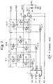
- Fig. 1 which illustrates a first prior art D/A converter (see: JP-A-2-311025)
- three-bit binary data signals D0, D1 and D2 are supplied to a decoder 1
- the decoder 1 generates seven-bit input signals IN1, IN2, ⁇ , IN7.
- Seven unit constant current cell circuits 2-1, 2-2, ⁇ , 2-7 are provided for the input signals IN1, IN2, ⁇ , IN7, respectively.
- the detail of the decoder 1 is illustrated in Fig. 2, and a truth table showing relationships between the inputs and outputs of the decoder 1 is shown in Fig. 3.
- each of the unit constant current cell circuits 2-1, 2-2, ⁇ , 2-7 includes P-channel MOS transistors 21, 22 and 23.
- the source of transistor 21 is connected to a high power supply terminal VDD, and a reference voltage VREF is applied to the gate of the transistor 21.
- the transistor 21 serves as a constant current source.
- the sources of the transistors 22 and 23 are connected to the drain of the transistor 21, and the drains of the transistors 22 and 23 are connected to output terminals OUT1 and OUT2, respectively.
- the gates of the transistors 22 and 23 are connected by the input signal such as IN1 and its inverted signal via an inverter sich as 3-1.
- the transistors 22 and 23 serve as current switching elements.
- the output terminals OUT1 and OUT2 are connected to external loads R1 and R2, respectively, which are grounded.
- a P-channel MOS transistor 41 as a switch is interposed between the drains of the transistors 22 and the output terminal OUT1
- a P-channel MOS transistor 42 as a switch is interposed between the drains of the transistors 23 and the output terminal OUT2.
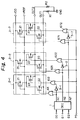
- Fig. 4 which illustrates a second prior art D/A converter (see: JP-A-2-311027)
- OR circuits 611, 612, 621, 622, ⁇ , 671, 672 are provided instead of the transistors 41 and 42 of Fig. 1.
- a current control signal PD is made high to turn OFF all the transistors 22 and 23.
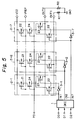
- a P-channel transistor 24 is added to each of the unit constant current cell circuits 2-1, 2-2, ⁇ , 2-7 of Fig. 1 instead of the transistors 41 and 42 of Fig. 1.
- a current control signal PD is made high to turn OFF all the transistors 24.
- Fig. 6 which illustrates a first embodiment of the present invention
- an operational amplifier 7 and a feedback circuit 8 are provided for controlling the transistors 21, instead of the transistors 41 and 42 of Fig. 1.
- a reference voltage VREF' is applied to an input (+) of the operational amplifier 7.
- the feedback circuit 8 includes a P-channel MOS transistor 81 corresponding to the transistor 21 and a resistor 82.
- the reference voltage VREF is controlled so that a voltage IVREF of the resistor 82, which is applied to an input (-) of the operational amplifier 7, is brought close to the reference voltage VREF'.
- a current control signal PD is supplied to the operational amplifier 7.
- all the transistors 21 as well as the transistor 81 are turned OFF.
- the current control signal PD and its inverted signal via an iverter 70 are supplied to the interior of the operational amplifier 7.
- the operational amplifier 7 is divided into a reference voltage generating circuit 71, a differential amplifier 72 and an output circuit 72.
- the reference voltage generating circuit 71 includes a diode-connected P-channel MOS transistor 711 and a diode-connected N-channel MOS transistor 712 connected in series between the power supply terminal VDD and a ground terminal GND.
- an N-channel MOS transistor 713 as a switch is interposed between the transistors 711 and 712
- a P-channel MOS transistor 714 as a switch is interposed between the power supply terminal VDD and the output of the reference voltage generating circuit 71.
- the transistors 713 and 714 are controlled by the inverted signal of the current control signal PD.
- the differential amplifier circuit 72 includes a P-channel MOS transistor 721 forming a mirror circuit with the transistor 711 of the reference voltage generating circuit 71, P-channel MOS transistors 722 and 723 controlled by the reference voltage VREF' and the voltage IVREF, and N-channel MOS transistors 724 and 725 forming a mirror circuit.
- the differential amplifier circuit 72 amplifies the difference between the reference voltage VREF' and the voltage IVREF.
- the output circuit 73 includes a P-channel MOS transistor 731 and an N-channel MOS transistor 732 connected in series between the power supply terminal VDD and a ground terminal GND.
- an P-channel MOS transistor 733 as a switch is interposed between the power supply terminal VDD and the output of the output circuit 73
- an N-channel MOS transistor 734 as a switch is interposed between the gate of the transistor 732 and the power supply terminal VDD.
- the transistor 733 is controlled by the inverted signal of the current control signal PD
- the transistor 734 is controlled by the current control signal PD.
- the operational amplifier 7 of Fig. 7 is operated in a normal operation mode.
- the transistors 713 and 714 are turned ON and OFF, respectively. Therefore, the reference voltage generates a reference voltage VST determined by the ON state transistors 711 and 712. As a result, the transistor 721 of the differential amplifier circuit 72 and the transistor 731 of the output circuit 73 forming the mirror circuits with the transistor 711 are in an ON state.
- the transistor 721 serves as a constant current source, and therefore, the difference between the reference voltage VREF' and the voltage IVREF is amplified and is transmitted to the gate of the transistor 732 of the output circuit 73.
- the transistors 733 and 734 are turned OFF. Therefore, the output of the differential amplifier 72 is further amplified in the output circuit 73 to obtain the reference voltage VREF.
- the operational amplifier 7 of Fig. 7 is operated in a low power consumption operation mode.
- the transistor 713 is turned OFF. Therefore, a current path between the power supply terminal VDD and the ground terminal GND in the reference voltage generating circuit 71 is cut OFF, to reduce the power dissipation. Also, the transistor 714 is turned ON, so that the reference voltage VST is pulled up to VDD. As a result, the transistor 721 of the differential amplifier circuit 72 and the transistor 731 of the output circuit 73 forming the mirror circuits with the transistor 711 are in an OFF state.
- the differential amplifier circuit 72 and the output circuit 73 are not operated to reduce the power dissipation.
- the transistor 733 is turned ON to pull up the reference voltage VREF to VDD, thus avoiding a high impedance state of the reference voltage VREF. Note that the high impedance state reference voltage VREF is unstable.
- the transistor 734 is turned ON, to turn OFF the transistor 732.
- a leakage current flowing through the transistor 732 is surely cut OFF, which also reduces the power dissipation.
- the transistors (constant current sources) 21 are turned ON. For example, if the input signals IN1, IN2, ⁇ , IN7 are low, all the transistors 22 are turned ON and all the transistors 23 are turned OFF, so that currents flowing through the transistors 21 are summed at the output terminal OUT1. Also, if the input signals IN1, IN2, ⁇ , IN7 are high, all the transistors 22 are turned OFF and all the transistors 23 are turned ON, so that currents flowing through the transistors 21 are summed at the output terminal OUT2.
- the reference voltage VREF is pulled up to VDD by the operational amplifier 7. Therefore, all the transistors 21 are turned OFF. Therefore, no current flows between the power supply terminal VDD and the ground terminal in the unit current cell circuits 2-1, 2-2, ⁇ , 2-7. Also, no leakage currents flow through the transistors 21. As a result, the power dissipation is reduced.
- a voltage divider formed by resistors R3 and R4 is provided instead of the inverters 3-1, 3-2, ⁇ , 3-7 of Fig. 6.
- a voltage VR determined by the voltage divider (R3, R4) is an intermediate level between a low level (GND) and a high level (VDD) of the input signals IN1, IN2, ⁇ , IN7. Therefore, in a normal operation mode, the D/A converter of Fig. 8 is operated in the same way as in the D/A converter of Fig. 6. In this case, since the voltage at the gates of the transistors 23 is constant, the noise characteristics are improved a compared with the D/A converter of Fig. 6.
- the D/A converter of Fig. 8 is advantageous with respect to the integration as compared with the D/A converter of Fig. 6.
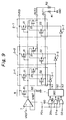
- OR circuits 100, 101 and 102 are added to the elements of Fig. 6.
- the OR circuits 100, 101 and 102 are controlled by the current control signal PD.
- PD normal operation mode
- the binary data signals D0, D1 and D2 pass through the OR circuits 100, 101 and 102 to the decoder 1.
- PD low power consumption mode
- all the outputs of the OR circuits 100, 101 and 102 are made "1" regardless of the binary data signals D0, D1 and D2.
- all the inputs of the decoder 1 are fixed at "1". Therefore, the state of the decoder 1 is fixed, thus reducing the power dissipation.
- Fig. 10 which illustrates a fourth embodiment of the present invention
- the D/A converter of Fig. 8 is combined with the D/A converter of Fig. 9.
- the power dissipation is further reduced.
- the polarities of the voltages of the power supply terminal VDD and the ground terminal GND can be reversed, and accordingly, the conductivity types of the transistors can be reversed.
- the power dissipation can be further reduced as compared with the prior art. Also, even if the number of input bits is increased, additional circuits for reducing the power dissipation are unnecessary, thus enhancing the integration.
Landscapes
- Engineering & Computer Science (AREA)
- Theoretical Computer Science (AREA)
- Analogue/Digital Conversion (AREA)
Priority Applications (1)
| Application Number | Priority Date | Filing Date | Title |
|---|---|---|---|
| EP01108084A EP1133061A1 (de) | 1995-04-21 | 1996-04-19 | Mit einem Operationsverstärker versehener Digital-Analog-Wandler vom Stromquellenmatrizentyp |
Applications Claiming Priority (3)
| Application Number | Priority Date | Filing Date | Title |
|---|---|---|---|
| JP9646395 | 1995-04-21 | ||
| JP7096463A JP2872074B2 (ja) | 1995-04-21 | 1995-04-21 | デジタル・アナログ変換装置 |
| JP96463/95 | 1995-04-21 |
Related Child Applications (1)
| Application Number | Title | Priority Date | Filing Date |
|---|---|---|---|
| EP01108084A Division EP1133061A1 (de) | 1995-04-21 | 1996-04-19 | Mit einem Operationsverstärker versehener Digital-Analog-Wandler vom Stromquellenmatrizentyp |
Publications (3)
| Publication Number | Publication Date |
|---|---|
| EP0739098A2 true EP0739098A2 (de) | 1996-10-23 |
| EP0739098A3 EP0739098A3 (de) | 1997-12-03 |
| EP0739098B1 EP0739098B1 (de) | 2002-07-31 |
Family
ID=14165731
Family Applications (2)
| Application Number | Title | Priority Date | Filing Date |
|---|---|---|---|
| EP96106211A Expired - Lifetime EP0739098B1 (de) | 1995-04-21 | 1996-04-19 | Mit einem Operationsverstärker versehener Digital-Analog-Wandler vom Stromquellenmatrizentyp |
| EP01108084A Withdrawn EP1133061A1 (de) | 1995-04-21 | 1996-04-19 | Mit einem Operationsverstärker versehener Digital-Analog-Wandler vom Stromquellenmatrizentyp |
Family Applications After (1)
| Application Number | Title | Priority Date | Filing Date |
|---|---|---|---|
| EP01108084A Withdrawn EP1133061A1 (de) | 1995-04-21 | 1996-04-19 | Mit einem Operationsverstärker versehener Digital-Analog-Wandler vom Stromquellenmatrizentyp |
Country Status (4)
| Country | Link |
|---|---|
| US (1) | US5706006A (de) |
| EP (2) | EP0739098B1 (de) |
| JP (1) | JP2872074B2 (de) |
| DE (1) | DE69622624T2 (de) |
Cited By (1)
| Publication number | Priority date | Publication date | Assignee | Title |
|---|---|---|---|---|
| EP1189353B1 (de) * | 2000-08-04 | 2007-02-28 | Matsushita Electric Industrial Co., Ltd. | D/A-Wandler |
Families Citing this family (10)
| Publication number | Priority date | Publication date | Assignee | Title |
|---|---|---|---|---|
| US6140860A (en) * | 1997-12-31 | 2000-10-31 | Intel Corporation | Thermal sensing circuit |
| KR20010086237A (ko) * | 1998-03-16 | 2001-09-10 | 가나이 쓰토무 | Da변환회로 |
| KR100459695B1 (ko) * | 2001-01-19 | 2004-12-03 | 삼성전자주식회사 | 소비전력이 적은 디지털 아날로그 변환기. |
| JPWO2004054114A1 (ja) * | 2002-12-10 | 2006-04-13 | 株式会社半導体エネルギー研究所 | 半導体装置、デジタル・アナログ変換回路及びそれらを用いた表示装置 |
| US6992608B2 (en) * | 2004-04-13 | 2006-01-31 | Texas Instruments Incorporated | Current-steering digital-to-analog converter having a minimum charge injection latch |
| JP4537840B2 (ja) * | 2004-12-13 | 2010-09-08 | 株式会社東芝 | 電流源セルおよびそれを用いたd/aコンバータ |
| JP2007227990A (ja) * | 2006-02-21 | 2007-09-06 | Oki Electric Ind Co Ltd | タイミング生成回路及びそれを用いたデジタル/アナログ変換器 |
| JP5418073B2 (ja) * | 2009-08-28 | 2014-02-19 | ソニー株式会社 | Da変換器及び固体撮像装置 |
| US8537040B2 (en) * | 2011-11-15 | 2013-09-17 | Integrated Device Technology, Inc. | Data converter current sources using thin-oxide core devices |
| KR20160041638A (ko) * | 2014-10-08 | 2016-04-18 | 에스케이하이닉스 주식회사 | 디지털 아날로그 컨버터 |
Family Cites Families (9)
| Publication number | Priority date | Publication date | Assignee | Title |
|---|---|---|---|---|
| JPS5672507A (en) * | 1979-11-19 | 1981-06-16 | Nec Corp | Current source circuit |
| US4381497A (en) * | 1981-04-03 | 1983-04-26 | Burr-Brown Research Corporation | Digital-to-analog converter having open-loop voltage reference for regulating bit switch currents |
| JPS58194425A (ja) * | 1982-05-07 | 1983-11-12 | Hitachi Ltd | D/a変換回路 |
| US4814688A (en) * | 1988-03-03 | 1989-03-21 | Brooktree Corporation | Reference generator |
| JP2794786B2 (ja) * | 1989-05-26 | 1998-09-10 | セイコーエプソン株式会社 | デジタル―アナログ変換回路 |
| JPH02311026A (ja) * | 1989-05-26 | 1990-12-26 | Seiko Epson Corp | デジタル―アナログ変換回路 |
| JPH02311025A (ja) * | 1989-05-26 | 1990-12-26 | Seiko Epson Corp | デジタル―アナログ変換回路 |
| US5023614A (en) * | 1989-09-13 | 1991-06-11 | Advanced Micro Devices, Inc. | Switchable DAC with current surge protection |
| US5294928A (en) * | 1992-08-31 | 1994-03-15 | Microchip Technology Incorporated | A/D converter with zero power mode |
-
1995
- 1995-04-21 JP JP7096463A patent/JP2872074B2/ja not_active Expired - Lifetime
-
1996
- 1996-04-19 EP EP96106211A patent/EP0739098B1/de not_active Expired - Lifetime
- 1996-04-19 DE DE69622624T patent/DE69622624T2/de not_active Expired - Lifetime
- 1996-04-19 EP EP01108084A patent/EP1133061A1/de not_active Withdrawn
- 1996-04-22 US US08/636,189 patent/US5706006A/en not_active Expired - Lifetime
Cited By (1)
| Publication number | Priority date | Publication date | Assignee | Title |
|---|---|---|---|---|
| EP1189353B1 (de) * | 2000-08-04 | 2007-02-28 | Matsushita Electric Industrial Co., Ltd. | D/A-Wandler |
Also Published As
| Publication number | Publication date |
|---|---|
| DE69622624D1 (de) | 2002-09-05 |
| JPH08293796A (ja) | 1996-11-05 |
| EP0739098A3 (de) | 1997-12-03 |
| JP2872074B2 (ja) | 1999-03-17 |
| DE69622624T2 (de) | 2003-03-27 |
| EP0739098B1 (de) | 2002-07-31 |
| EP1133061A1 (de) | 2001-09-12 |
| US5706006A (en) | 1998-01-06 |
Similar Documents
| Publication | Publication Date | Title |
|---|---|---|
| US5907259A (en) | Operational amplification circuit capable of driving a high load | |
| US6781449B2 (en) | Electronic output stage | |
| JP2993462B2 (ja) | 出力バッファ回路 | |
| JP3079515B2 (ja) | ゲ−トアレイ装置及び入力回路及び出力回路及び降圧回路 | |
| US8063808B2 (en) | Multi-input operational amplifier circuit, digital/analog converter using same, and driver for display device using same | |
| US6275073B1 (en) | Differential input circuit | |
| US5909187A (en) | Current steering circuit for a digital-to-analog converter | |
| US5706006A (en) | Operational amplifier incorporating current matrix type digital-to-analog converter | |
| US5929679A (en) | Voltage monitoring circuit capable of reducing power dissipation | |
| US5235218A (en) | Switching constant current source circuit | |
| JP3003625B2 (ja) | Cmlcmos変換回路 | |
| US7304458B2 (en) | Regulator circuit | |
| US6275179B1 (en) | Digital to analog converter using a current matrix system | |
| US7250793B2 (en) | Low voltage differential signaling driving apparatus | |
| US5302951A (en) | Wide-range linear output digital/analog converter | |
| JPH09246885A (ja) | 入力回路及びオペアンプ回路並びに半導体集積回路装置 | |
| US7277036B2 (en) | Digital-to-analog converting circuit | |
| KR100280951B1 (ko) | 출력 전류 변동을 억합할 수 있는 전류 출력형 디지털-아날로그 변환기 | |
| KR100223849B1 (ko) | 반도체 메모리장치 | |
| JPH0677804A (ja) | 出力回路 | |
| US5945851A (en) | Current source apparatus with bias switches | |
| JP3855810B2 (ja) | 差動増幅回路 | |
| US6329842B1 (en) | Output circuit for electronic devices | |
| KR0183925B1 (ko) | 디지털 아날로그 변환기의 스위치 장치 | |
| US6518819B2 (en) | Push-pull output stage for digital signals with regulated output levels |
Legal Events
| Date | Code | Title | Description |
|---|---|---|---|
| PUAI | Public reference made under article 153(3) epc to a published international application that has entered the european phase |
Free format text: ORIGINAL CODE: 0009012 |
|
| AK | Designated contracting states |
Kind code of ref document: A2 Designated state(s): DE FR GB |
|
| PUAL | Search report despatched |
Free format text: ORIGINAL CODE: 0009013 |
|
| AK | Designated contracting states |
Kind code of ref document: A3 Designated state(s): DE FR GB |
|
| 17P | Request for examination filed |
Effective date: 19980309 |
|
| 17Q | First examination report despatched |
Effective date: 20001206 |
|
| GRAG | Despatch of communication of intention to grant |
Free format text: ORIGINAL CODE: EPIDOS AGRA |
|
| GRAG | Despatch of communication of intention to grant |
Free format text: ORIGINAL CODE: EPIDOS AGRA |
|
| GRAH | Despatch of communication of intention to grant a patent |
Free format text: ORIGINAL CODE: EPIDOS IGRA |
|
| GRAH | Despatch of communication of intention to grant a patent |
Free format text: ORIGINAL CODE: EPIDOS IGRA |
|
| GRAA | (expected) grant |
Free format text: ORIGINAL CODE: 0009210 |
|
| AK | Designated contracting states |
Kind code of ref document: B1 Designated state(s): DE FR GB |
|
| REG | Reference to a national code |
Ref country code: GB Ref legal event code: FG4D |
|
| REF | Corresponds to: |
Ref document number: 69622624 Country of ref document: DE Date of ref document: 20020905 |
|
| ET | Fr: translation filed | ||
| REG | Reference to a national code |
Ref country code: GB Ref legal event code: 732E |
|
| PLBE | No opposition filed within time limit |
Free format text: ORIGINAL CODE: 0009261 |
|
| STAA | Information on the status of an ep patent application or granted ep patent |
Free format text: STATUS: NO OPPOSITION FILED WITHIN TIME LIMIT |
|
| 26N | No opposition filed |
Effective date: 20030506 |
|
| REG | Reference to a national code |
Ref country code: FR Ref legal event code: TP |
|
| REG | Reference to a national code |
Ref country code: FR Ref legal event code: CD |
|
| REG | Reference to a national code |
Ref country code: DE Ref legal event code: R082 Ref document number: 69622624 Country of ref document: DE Representative=s name: BETTEN & RESCH, DE |
|
| REG | Reference to a national code |
Ref country code: DE Ref legal event code: R082 Ref document number: 69622624 Country of ref document: DE Representative=s name: BETTEN & RESCH PATENT- UND RECHTSANWAELTE PART, DE Effective date: 20120828 Ref country code: DE Ref legal event code: R082 Ref document number: 69622624 Country of ref document: DE Representative=s name: PATENTANWAELTE BETTEN & RESCH, DE Effective date: 20120828 Ref country code: DE Ref legal event code: R081 Ref document number: 69622624 Country of ref document: DE Owner name: RENESAS ELECTRONICS CORPORATION, KAWASAKI-SHI, JP Free format text: FORMER OWNER: NEC ELECTRONICS CORP., KAWASAKI, KANAGAWA, JP Effective date: 20120828 Ref country code: DE Ref legal event code: R081 Ref document number: 69622624 Country of ref document: DE Owner name: RENESAS ELECTRONICS CORPORATION, JP Free format text: FORMER OWNER: NEC ELECTRONICS CORP., KAWASAKI, JP Effective date: 20120828 |
|
| PGFP | Annual fee paid to national office [announced via postgrant information from national office to epo] |
Ref country code: DE Payment date: 20130508 Year of fee payment: 18 Ref country code: GB Payment date: 20130417 Year of fee payment: 18 |
|
| PGFP | Annual fee paid to national office [announced via postgrant information from national office to epo] |
Ref country code: FR Payment date: 20130625 Year of fee payment: 18 |
|
| REG | Reference to a national code |
Ref country code: DE Ref legal event code: R119 Ref document number: 69622624 Country of ref document: DE |
|
| GBPC | Gb: european patent ceased through non-payment of renewal fee |
Effective date: 20140419 |
|
| REG | Reference to a national code |
Ref country code: FR Ref legal event code: ST Effective date: 20141231 |
|
| REG | Reference to a national code |
Ref country code: DE Ref legal event code: R119 Ref document number: 69622624 Country of ref document: DE Effective date: 20141101 |
|
| PG25 | Lapsed in a contracting state [announced via postgrant information from national office to epo] |
Ref country code: DE Free format text: LAPSE BECAUSE OF NON-PAYMENT OF DUE FEES Effective date: 20141101 Ref country code: GB Free format text: LAPSE BECAUSE OF NON-PAYMENT OF DUE FEES Effective date: 20140419 |
|
| PG25 | Lapsed in a contracting state [announced via postgrant information from national office to epo] |
Ref country code: FR Free format text: LAPSE BECAUSE OF NON-PAYMENT OF DUE FEES Effective date: 20140430 |