EP0740073B1 - Circuit pour détecter une surtension dans un charge électrique - Google Patents
Circuit pour détecter une surtension dans un charge électrique Download PDFInfo
- Publication number
- EP0740073B1 EP0740073B1 EP95830168A EP95830168A EP0740073B1 EP 0740073 B1 EP0740073 B1 EP 0740073B1 EP 95830168 A EP95830168 A EP 95830168A EP 95830168 A EP95830168 A EP 95830168A EP 0740073 B1 EP0740073 B1 EP 0740073B1
- Authority
- EP
- European Patent Office
- Prior art keywords
- voltage
- output
- input terminal
- overvoltage
- output terminal
- Prior art date
- Legal status (The legal status is an assumption and is not a legal conclusion. Google has not performed a legal analysis and makes no representation as to the accuracy of the status listed.)
- Expired - Lifetime
Links
Images

Classifications
-
- H—ELECTRICITY
- H01—ELECTRIC ELEMENTS
- H01T—SPARK GAPS; OVERVOLTAGE ARRESTERS USING SPARK GAPS; SPARKING PLUGS; CORONA DEVICES; GENERATING IONS TO BE INTRODUCED INTO NON-ENCLOSED GASES
- H01T13/00—Sparking plugs
- H01T13/58—Testing
- H01T13/60—Testing of electrical properties
-
- F—MECHANICAL ENGINEERING; LIGHTING; HEATING; WEAPONS; BLASTING
- F02—COMBUSTION ENGINES; HOT-GAS OR COMBUSTION-PRODUCT ENGINE PLANTS
- F02P—IGNITION, OTHER THAN COMPRESSION IGNITION, FOR INTERNAL-COMBUSTION ENGINES; TESTING OF IGNITION TIMING IN COMPRESSION-IGNITION ENGINES
- F02P17/00—Testing of ignition installations, e.g. in combination with adjusting; Testing of ignition timing in compression-ignition engines
- F02P17/12—Testing characteristics of the spark, ignition voltage or current
-
- G—PHYSICS
- G01—MEASURING; TESTING
- G01R—MEASURING ELECTRIC VARIABLES; MEASURING MAGNETIC VARIABLES
- G01R29/00—Arrangements for measuring or indicating electric quantities not covered by groups G01R19/00 - G01R27/00
- G01R29/02—Measuring characteristics of individual pulses, e.g. deviation from pulse flatness, rise time or duration
- G01R29/027—Indicating that a pulse characteristic is either above or below a predetermined value or within or beyond a predetermined range of values
- G01R29/0273—Indicating that a pulse characteristic is either above or below a predetermined value or within or beyond a predetermined range of values the pulse characteristic being duration, i.e. width (indicating that frequency of pulses is above or below a certain limit)
Definitions
- This invention relates to a circuit for detecting overvoltage on an electrical load inserted between a feed line and a controlled switch.
- the field of application of the invention relates in particular to the motor vehicle industry and the description which follows is made with reference to a circuit to detect an overvoltage in a coil inserted between a feed line and a controlled switch, solely for the purpose of simplifying the description.
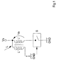
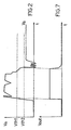
- control switch S opens, voltage Va present in the primary circuit L' of ignition coil L increases rapidly and then stops, after a certain time interval, at a value equal to that of the voltage Vs provided by the vehicle's battery.
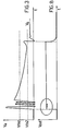
- the time for which the overvoltage lasts is approximately 100 ⁇ s.
- the technical problem underlying this invention is that of providing a circuit for correct and accurate determination of a time duration of an overvoltage on an electrical load between a feed line and a controlled switch.
- 1 indicates as a whole a circuit for detecting an overvoltage in an electrical load Z1 inserted with a first and a second terminal between a feed line AL and a controlled switch S.
- circuit 1 comprises a first threshold comparator C1 which has a first input terminal held at a first reference voltage E1, a second input terminal connected to feed line AL and an output terminal.
- circuit 1 also includes a second threshold comparator C2 which has a first input terminal held at a second reference voltage E2.
- This second comparator C2 also includes a second input terminal connected to the second terminal of electrical load Z1 through a one-way block ZN which is connected in series to a first resistance element R1, and an output terminal.
- the second input terminal of comparator C2 is also connected to a fourth reference voltage GND, for example a ground, through a third resistance element R2.
- Circuit 1 also includes an output transistor T1, for example of the NPN type, inserted with a first and a second terminal between feed line AL and an output terminal OUT from circuit 1.
- an output transistor T1 for example of the NPN type, inserted with a first and a second terminal between feed line AL and an output terminal OUT from circuit 1.
- This transistor T1 is controlled by means of a logic block D which has input connected to the output terminals of threshold comparators C1 and C2.
- Circuit 1 also includes a feedback block R inserted with an input terminal and an output terminal respectively between the output terminal OUT of circuit 1 and a further input to logic block D.
- this feedback block R includes a third threshold comparator C3 which has a first input terminal held at a third reference voltage E3, a second input terminal connected to the output terminal OUT of circuit 1 and an output terminal.
- logic block D includes a first logic gate P1, for example of the OR type, which has a first input terminal connected to the output terminal of the second threshold comparator C2 and a second input terminal connected to the output terminal of the third threshold comparator C3.
- logic block D also includes a second logic gate P2, for example of the AND type, having a first input terminal connected to the output terminal of first comparator C1 and a second input terminal connected to the output terminal of first logic gate P1.
- a second logic gate P2 for example of the AND type, having a first input terminal connected to the output terminal of first comparator C1 and a second input terminal connected to the output terminal of first logic gate P1.
- This second logic gate P2 also includes an output terminal by means of which output transistor T1 is controlled.
- Figure 4 shows that a condenser C1, which is connected in parallel to a second resistance element R1, is inserted between the output terminal OUT of circuit 1 and the fourth reference voltage GND.
- circuit 1 For convenience of description, the operation of circuit 1 according to the invention will now be described with reference to an application in which electrical load Z1 is of the inductive type, for example an engine's electronic ignition coil L comprising a primary circuit L' and a secondary circuit L'', as shown in Figure 5.
- electrical load Z1 is of the inductive type, for example an engine's electronic ignition coil L comprising a primary circuit L' and a secondary circuit L'', as shown in Figure 5.
- the peak value of voltage Va is approximately 400 V if a spark is absent and approximately 250 V if a spark is present.
- V1 > Vs + E1 Vth2
- V1 V2 + Vzn
- Vs the supply voltage, which in this application is the same as the vehicle's battery voltage, and lies between approximately 6V and approximately 24V
- E1 is of the order of a few volts
- Vth2 is a second lower threshold value.
- Voltage Vc2 activates logic gate P1 to provide an output voltage Vp1 which is itself at a high logic level.
- logic gate P2 has a high logic level on both its inputs it is activated to provide an output voltage Vp2 which is also at a high logic level.
- This voltage Vp2 causes output transistor T1 to become active.
- third threshold comparator C3 performs a switching operation, providing a voltage Vc3 at a high logic level as an output.
- logic gate P1 has both inputs at a high logic level it continues to maintain voltage Vp1 at a high logic level.
- voltage Vout remains at the value Vp2-VbeT1 and condenser C1 remains charged.
- third threshold comparator C3 maintains voltage Vc3 at a high logic level and there is still a voltage Vp1 at a high logic level at the output from logic gate P1.
- logic gate P2 still has inputs at a high logic level, it maintains voltage Vp2 at a high logic level, and as a consequence output transistor T1 remains active.
- Va V1 ⁇ Vth2 first threshold comparator C1 switches, reducing voltage Vc1 to zero.
- logic gate P2 also switches, reducing voltage Vp2 to zero and deactivating output transistor T1.
- third comparator C3 in fact maintains voltage Vc3 at a high logic level.
- logic gate P2 is activated again to provide an output voltage Vp2 at a high logic level, which reactivates output transistor T1.
- circuit 1 and controlled switch S which is constructed for example using a power transistor, are incorporated into the same silicon chip using technology of the VIPower type.
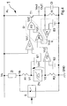
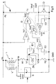
- Figure 6 shows a preferred embodiment of circuit 1 according to the invention.
- one-way block ZN comprises a first diode, Z1, a second Z2, a third Z3 and a fourth Z4, of the Zener, type which are connected together in series.
- First threshold comparator C1 comprises a second transistor T2, of the PNP type, while second threshold comparator C2 and first logic gate P1 are provided by a third transistor T3, of the NPN type.
- a fifth diode D1 is connected to an emitter terminal of second transistor T2 to provide first reference voltage E1.
- Figure 6 also shows that second logic gate P2 is provided by a fourth transistor T4, of the NPN type, while a fifth transistor T5 and a sixth T6, of the PNP type, in a mirror-current connection, provide third threshold comparator C3.
- circuit 1 as shown in Figure 6 also comprises a sixth diode Z5 of the Zener type, inserted with a first and a second terminal between a drive terminal first output transistor T1 and a ground.
- second transistor T2 also becomes active providing an output current which causes first transistor T1 to become active.
- diode Z5 causes voltage Vout not to exceed a maximum value of Vz5-VbeT1.
- Va ⁇ Vs + VbeT2 + VD1 obtains, second transistor T2 is deactivated, and no longer provides any current to first transistor T1, which is in turn deactivated.
- third transistor T3 keeps fourth transistor T4 inactive.
- voltage Vout again adopts a value which is greater than zero.
- third transistor T3 also becomes inactive, while fourth transistor T4 becomes active, rendering first transistor T1 definitively inactive.
- Zener diodes Z1, Z2, Z3, Z4 can only be made active again when voltage Va again exceeds voltage Vzn, reactivating the chain of Zener diodes Z1, Z2, Z3, Z4.
Landscapes
- Engineering & Computer Science (AREA)
- Chemical & Material Sciences (AREA)
- Combustion & Propulsion (AREA)
- Physics & Mathematics (AREA)
- General Physics & Mathematics (AREA)
- Mechanical Engineering (AREA)
- General Engineering & Computer Science (AREA)
- Emergency Protection Circuit Devices (AREA)
- Measurement Of Current Or Voltage (AREA)
- Ignition Installations For Internal Combustion Engines (AREA)
- Electronic Switches (AREA)
Claims (9)
- Circuit de détection de la durée de temps d'un signal de surtension (Va) sur une charge électrique (Z1) inséré, avec des première et deuxième bornes, entre une ligne d'alimentation (AL) et un interrupteur de commande (S), ledit circuit ayant un signal de tension en sortie (Vout) à une borne de sortie (OUT) et comprenant :au moins un premier comparateur à seuil (C1) ayant une première borne d'entrée recevant une tension indicative de la surtension (Va), ladite tension comprenant une première tension de référence (E1) appliquée à ladite première borne d'entrée, une deuxième borne d'entrée couplée à la ligne d'alimentation (AL) et une borne de sortie pour produire un premier signal de tension (Vc1) à un premier niveau logique, lorsque le signal de surtension (Va) dépasse une deuxième tension de seuil (Vth2), et à un deuxième niveau logique, lorsque le signal de surtension (Va) chute au-dessous de la deuxième tension de seuil (Vth2) ;au moins un deuxième comparateur à seuil (C2) ayant une première borne d'entrée maintenue à une deuxième tension de référence (E2), une deuxième borne d'entrée recevant une tension indicative de la surtension (Va) et une borne de sortie pour produire un deuxième signal de tension (Vc2) à un premier niveau logique, lorsque le signal de surtension (Va) dépasse une première tension de seuil (Vth1), et à un deuxième niveau logique, lorsque le signal de surtension (Va) chute au-dessous de la première tension de seuil (Vth1) ;au moins un transistor de sortie (T1) inséré, avec des première et deuxième bornes, entre une ligne d'alimentation (AL) et la borne de sortie (OUT) pour produire le signal de tension en sortie (Vout), ledit transistor (T1) étant connecté à au moins un bloc logique (D) comportant des entrées connectées aux sorties des comparateurs à seuil (C1) et (C2), ledit bloc logique (D) servant à commander le transistor de sortie (T1) de manière à faire en sorte que le signal de tension en sortie (Vout) soit au premier niveau logique, lorsque le premier (Vc1) et le deuxième (Vc2) signal de tension sont au premier niveau logique ;au moins un bloc de rétroaction (R) inséré, avec une borne d'entrée et une borne de sortie, respectivement entre la borne de sortie (OUT) et une autre borne d'entrée du bloc logique (D), ledit bloc de rétroaction (R) servant à maintenir le signal de tension en sortie (Vout) au premier niveau logique, pendant un intervalle de temps suffisant pour supprimer des variations dudit niveau logique, qui seraient dues à des variations rapides de la surtension (Va), ladite durée de temps étant détectée par la condition Va < Vth2 persistant pendant un temps suffisamment long pour effectuer une distinction entre des variations rapides et une durée de surtension régulière, au cours de la durée de temps du signal de surtension (Va).
- Circuit selon la revendication 1, caractérisé en ce que le bloc de rétroaction (R) comprend au moins un troisième comparateur à seuil (C3) ayant une première borne d'entrée maintenue à une troisième tension de référence (E3), une deuxième borne d'entrée connectée à la borne de sortie (OUT) du circuit (1) et une borne de sortie.
- Circuit selon la revendication 1, caractérisé en ce que le bloc logique (D) comprend :au moins une première porte logique (P1) ayant une première borne d'entrée connectée à la borne de sortie du deuxième comparateur à seuil (C2), une deuxième borne d'entrée connectée à la borne de sortie du troisième comparateur à seuil (C3) et une borne de sortie ;au moins une deuxième porte logique (P2) ayant une première borne d'entrée connectée à la borne de sortie du premier comparateur (C1), une deuxième borne d'entrée connectée à la borne de sortie de la première porte logique (P1) et une borne de sortie susceptible de commander le transistor de sortie (T1).
- Circuit selon la revendication 1, caractérisé en ce que la deuxième borne d'entrée du deuxième comparateur (C2) est connectée à la deuxième borne de la charge électrique (Z1) par l'intermédiaire d'au moins un bloc unidirectionnel (ZN) connecté en série à un premier élément de résistance (R1).
- Circuit selon la revendication 1, caractérisé en ce qu'un condensateur (C1), connecté en parallèle à un deuxième élément de résistance (R1), est inséré entre sa borne de sortie (OUT) et une quatrième tension de référence (GND).
- Circuit selon la revendication 3, caractérisé en ce que la première porte logique (P1) est de type OU.
- Circuit selon la revendication 3, caractérisé en ce que la deuxième porte logique (P2) est de type ET.
- Circuit selon la revendication 1, caractérisé en ce que le transistor de sortie (T1) est de type NPN.
- Circuit selon la revendication 1, caractérisé en ce qu'il est intégré en utilisant une technologie de type VIP de puissance.
Priority Applications (4)
| Application Number | Priority Date | Filing Date | Title |
|---|---|---|---|
| EP95830168A EP0740073B1 (fr) | 1995-04-28 | 1995-04-28 | Circuit pour détecter une surtension dans un charge électrique |
| DE69533391T DE69533391D1 (de) | 1995-04-28 | 1995-04-28 | Schaltung zur Erkennung einer Überspannung an einem elektrischen Verbraucher |
| JP8105533A JPH08304480A (ja) | 1995-04-28 | 1996-04-25 | 過電圧検出回路 |
| US08/639,794 US5735254A (en) | 1995-04-28 | 1996-04-29 | Circuit for detecting an overvoltage on a switched inductive load |
Applications Claiming Priority (1)
| Application Number | Priority Date | Filing Date | Title |
|---|---|---|---|
| EP95830168A EP0740073B1 (fr) | 1995-04-28 | 1995-04-28 | Circuit pour détecter une surtension dans un charge électrique |
Publications (2)
| Publication Number | Publication Date |
|---|---|
| EP0740073A1 EP0740073A1 (fr) | 1996-10-30 |
| EP0740073B1 true EP0740073B1 (fr) | 2004-08-18 |
Family
ID=8221907
Family Applications (1)
| Application Number | Title | Priority Date | Filing Date |
|---|---|---|---|
| EP95830168A Expired - Lifetime EP0740073B1 (fr) | 1995-04-28 | 1995-04-28 | Circuit pour détecter une surtension dans un charge électrique |
Country Status (4)
| Country | Link |
|---|---|
| US (1) | US5735254A (fr) |
| EP (1) | EP0740073B1 (fr) |
| JP (1) | JPH08304480A (fr) |
| DE (1) | DE69533391D1 (fr) |
Families Citing this family (12)
| Publication number | Priority date | Publication date | Assignee | Title |
|---|---|---|---|---|
| KR100486351B1 (ko) * | 1997-11-13 | 2005-07-07 | 페어차일드코리아반도체 주식회사 | 과부하 보호기능을 갖는 펄스폭 변조 제어장치 |
| DE60015711T2 (de) * | 2000-01-27 | 2005-11-24 | Stmicroelectronics S.R.L., Agrate Brianza | Elektronische Zündungseinheit mit Beschränkung der Spannung an eine Anschluss der Zündungspulenprimärwicklung |
| EP1184954A1 (fr) * | 2000-08-31 | 2002-03-06 | STMicroelectronics S.r.l. | Régulateur de tension intégré et auto-alimenté et le procédé de régulation correspondant |
| JP3607902B2 (ja) * | 2002-07-22 | 2005-01-05 | 三菱電機株式会社 | 内燃機関用点火装置 |
| DE10243858A1 (de) * | 2002-09-20 | 2004-04-01 | Siemens Ag | Netzüberspannungsschutz |
| FR2853941B1 (fr) * | 2003-04-17 | 2007-02-09 | Siemens Vdo Automotive | Procede de controle du courant primaire d'allumage d'un moteur a combustion interne a allumage commande |
| DE602006006978D1 (de) * | 2005-02-09 | 2009-07-09 | Nxp Bv | Verfahren zur sicherstellung einer sicheren nfc-funktionalität einer drahtlosen mobilen kommunikationsvorrichtung und drahtlose mobile kommunikationsvorrichtung mit sicherer nfc-funktionalität |
| US20100006066A1 (en) * | 2008-07-14 | 2010-01-14 | Nicholas Danne | Variable primary current for ionization |
| US8342151B2 (en) * | 2008-12-18 | 2013-01-01 | GM Global Technology Operations LLC | Deactivation of high pressure pump for noise control |
| CN101557099B (zh) * | 2009-05-12 | 2011-09-21 | 中兴通讯股份有限公司 | 模块电源短路保护电路 |
| JP5664327B2 (ja) * | 2011-02-23 | 2015-02-04 | 富士電機株式会社 | Dc−dcコンバータの制御装置 |
| CN105422360B (zh) * | 2015-11-30 | 2017-12-15 | 深圳市轱辘车联数据技术有限公司 | 一种汽车点火动作的检测电路 |
Family Cites Families (14)
| Publication number | Priority date | Publication date | Assignee | Title |
|---|---|---|---|---|
| DE3071012D1 (en) * | 1979-05-25 | 1985-09-26 | Lucas Ind Plc | A test procedure for testing an internal combustion engine electronic ignition system |
| US4380989A (en) * | 1979-11-27 | 1983-04-26 | Nippondenso Co., Ltd. | Ignition system for internal combustion engine |
| US4604750A (en) * | 1983-11-07 | 1986-08-05 | Digital Equipment Corporation | Pipeline error correction |
| US4612640A (en) * | 1984-02-21 | 1986-09-16 | Seeq Technology, Inc. | Error checking and correction circuitry for use with an electrically-programmable and electrically-erasable memory array |
| US4750467A (en) * | 1986-09-11 | 1988-06-14 | General Motors Corporation | Internal combustion engine ignition system |
| JP2606862B2 (ja) * | 1987-12-28 | 1997-05-07 | 株式会社東芝 | 単−エラー検出・訂正方式 |
| JP2583547B2 (ja) * | 1988-01-13 | 1997-02-19 | 株式会社日立製作所 | 半導体メモリ |
| US4886029A (en) * | 1988-05-26 | 1989-12-12 | Motorola Inc. | Ignition misfire detector |
| US4918389A (en) * | 1988-06-03 | 1990-04-17 | Robert Bosch Gmbh | Detecting misfiring in spark ignition engines |
| JP2664236B2 (ja) * | 1989-02-01 | 1997-10-15 | 富士通株式会社 | 半導体記憶装置 |
| DE3907616A1 (de) * | 1989-03-09 | 1990-09-20 | Bosch Gmbh Robert | Schaltungsanordnung zur messung der primaerspannung einer zuendspule |
| DE4107335A1 (de) * | 1991-03-07 | 1992-09-10 | Beru Werk Ruprecht Gmbh Co A | Verfahren und vorrichtung zur zuendueberwachung einer zuendanlage |
| US5309888A (en) * | 1991-08-02 | 1994-05-10 | Motorola, Inc. | Ignition system |
| US5446385A (en) * | 1992-10-02 | 1995-08-29 | Robert Bosch Gmbh | Ignition system for internal combustion engines |
-
1995
- 1995-04-28 EP EP95830168A patent/EP0740073B1/fr not_active Expired - Lifetime
- 1995-04-28 DE DE69533391T patent/DE69533391D1/de not_active Expired - Lifetime
-
1996
- 1996-04-25 JP JP8105533A patent/JPH08304480A/ja active Pending
- 1996-04-29 US US08/639,794 patent/US5735254A/en not_active Expired - Lifetime
Also Published As
| Publication number | Publication date |
|---|---|
| EP0740073A1 (fr) | 1996-10-30 |
| DE69533391D1 (de) | 2004-09-23 |
| JPH08304480A (ja) | 1996-11-22 |
| US5735254A (en) | 1998-04-07 |
Similar Documents
| Publication | Publication Date | Title |
|---|---|---|
| EP0740073B1 (fr) | Circuit pour détecter une surtension dans un charge électrique | |
| EP0366622A2 (fr) | Circuit de commande de charges inductives, en particulier pour actionner des injecteurs électriques d'un moteur diesel | |
| US6556407B2 (en) | Method and device for driving a power output stage | |
| EP0763882B1 (fr) | Dispositif d'attaque de charge | |
| US7525783B2 (en) | Monitoring method for an actuator and corresponding driver circuit | |
| EP0297584B1 (fr) | Système d'allumage pour moteur à combustion interne | |
| US4520420A (en) | Current control method and apparatus for electromagnetic valves | |
| US6060814A (en) | Device and method for driving at least one capacitive actuator | |
| US6137208A (en) | Device and method for driving a capacitive actuator | |
| US4314305A (en) | Solenoid drive circuits | |
| US6456156B1 (en) | Method and device for the open-load diagnosis of a switching stage | |
| KR100349093B1 (ko) | 하나 이상의 용량형 액츄에이터를 구동하기 위한 장치 및 방법 | |
| US6531908B1 (en) | Power output stage for switching inductive loads with reduced radiation emission | |
| EP0924589A1 (fr) | Appareil de commande pour un actionneur électrique et méthode pour commander cet appareil de commande | |
| US5218339A (en) | Arrangement for monitoring a consumer in combination with an internal combustion engine and/or a motor vehicle | |
| US4246881A (en) | System for decreasing the power consumption in the output transistor of an ignition system | |
| US20020144544A1 (en) | Automotive ignition monitoring system with misfire and fouled plug detection | |
| WO1987007451A1 (fr) | Appareil de protection contre des defauts | |
| US4461979A (en) | Low-drive power switching transistor control circuit | |
| JP2000110640A (ja) | 電磁弁駆動装置 | |
| US5828141A (en) | Apparatus for switching an inductive load | |
| EP0590223B1 (fr) | Procédé et dispositif de récupération d'énergie dans le pilotage de charges inductives | |
| US4097770A (en) | SCR trigger circuit | |
| EP0896757A1 (fr) | Dispositif comprenant un transistor de commutation protege thermiquement | |
| US4105006A (en) | Ignition system for internal combustion engine |
Legal Events
| Date | Code | Title | Description |
|---|---|---|---|
| PUAI | Public reference made under article 153(3) epc to a published international application that has entered the european phase |
Free format text: ORIGINAL CODE: 0009012 |
|
| AK | Designated contracting states |
Kind code of ref document: A1 Designated state(s): DE FR GB IT |
|
| 17P | Request for examination filed |
Effective date: 19970421 |
|
| 17Q | First examination report despatched |
Effective date: 19970924 |
|
| RAP3 | Party data changed (applicant data changed or rights of an application transferred) |
Owner name: STMICROELECTRONICS S.R.L. Owner name: CO.RI.M.ME. CONSORZIO PER LA RICERCA SULLA MICROEL |
|
| GRAP | Despatch of communication of intention to grant a patent |
Free format text: ORIGINAL CODE: EPIDOSNIGR1 |
|
| GRAS | Grant fee paid |
Free format text: ORIGINAL CODE: EPIDOSNIGR3 |
|
| GRAA | (expected) grant |
Free format text: ORIGINAL CODE: 0009210 |
|
| AK | Designated contracting states |
Kind code of ref document: B1 Designated state(s): DE FR GB IT |
|
| PG25 | Lapsed in a contracting state [announced via postgrant information from national office to epo] |
Ref country code: FR Free format text: LAPSE BECAUSE OF FAILURE TO SUBMIT A TRANSLATION OF THE DESCRIPTION OR TO PAY THE FEE WITHIN THE PRESCRIBED TIME-LIMIT Effective date: 20040818 |
|
| REG | Reference to a national code |
Ref country code: GB Ref legal event code: FG4D |
|
| REF | Corresponds to: |
Ref document number: 69533391 Country of ref document: DE Date of ref document: 20040923 Kind code of ref document: P |
|
| PG25 | Lapsed in a contracting state [announced via postgrant information from national office to epo] |
Ref country code: DE Free format text: LAPSE BECAUSE OF FAILURE TO SUBMIT A TRANSLATION OF THE DESCRIPTION OR TO PAY THE FEE WITHIN THE PRESCRIBED TIME-LIMIT Effective date: 20041119 |
|
| PG25 | Lapsed in a contracting state [announced via postgrant information from national office to epo] |
Ref country code: IT Free format text: LAPSE BECAUSE OF NON-PAYMENT OF DUE FEES;WARNING: LAPSES OF ITALIAN PATENTS WITH EFFECTIVE DATE BEFORE 2007 MAY HAVE OCCURRED AT ANY TIME BEFORE 2007. THE CORRECT EFFECTIVE DATE MAY BE DIFFERENT FROM THE ONE RECORDED. Effective date: 20050428 |
|
| PLBE | No opposition filed within time limit |
Free format text: ORIGINAL CODE: 0009261 |
|
| STAA | Information on the status of an ep patent application or granted ep patent |
Free format text: STATUS: NO OPPOSITION FILED WITHIN TIME LIMIT |
|
| 26N | No opposition filed |
Effective date: 20050519 |
|
| EN | Fr: translation not filed | ||
| PGFP | Annual fee paid to national office [announced via postgrant information from national office to epo] |
Ref country code: GB Payment date: 20070328 Year of fee payment: 13 |
|
| GBPC | Gb: european patent ceased through non-payment of renewal fee |
Effective date: 20080428 |
|
| PG25 | Lapsed in a contracting state [announced via postgrant information from national office to epo] |
Ref country code: GB Free format text: LAPSE BECAUSE OF NON-PAYMENT OF DUE FEES Effective date: 20080428 |