EP0740186A2 - Unité d'affichage à cristal liquide - Google Patents
Unité d'affichage à cristal liquide Download PDFInfo
- Publication number
- EP0740186A2 EP0740186A2 EP96301357A EP96301357A EP0740186A2 EP 0740186 A2 EP0740186 A2 EP 0740186A2 EP 96301357 A EP96301357 A EP 96301357A EP 96301357 A EP96301357 A EP 96301357A EP 0740186 A2 EP0740186 A2 EP 0740186A2
- Authority
- EP
- European Patent Office
- Prior art keywords
- liquid crystal
- spacers
- pixel array
- substrate
- array region
- Prior art date
- Legal status (The legal status is an assumption and is not a legal conclusion. Google has not performed a legal analysis and makes no representation as to the accuracy of the status listed.)
- Withdrawn
Links
Images


Classifications
-
- G—PHYSICS
- G02—OPTICS
- G02F—OPTICAL DEVICES OR ARRANGEMENTS FOR THE CONTROL OF LIGHT BY MODIFICATION OF THE OPTICAL PROPERTIES OF THE MEDIA OF THE ELEMENTS INVOLVED THEREIN; NON-LINEAR OPTICS; FREQUENCY-CHANGING OF LIGHT; OPTICAL LOGIC ELEMENTS; OPTICAL ANALOGUE/DIGITAL CONVERTERS
- G02F1/00—Devices or arrangements for the control of the intensity, colour, phase, polarisation or direction of light arriving from an independent light source, e.g. switching, gating or modulating; Non-linear optics
- G02F1/01—Devices or arrangements for the control of the intensity, colour, phase, polarisation or direction of light arriving from an independent light source, e.g. switching, gating or modulating; Non-linear optics for the control of the intensity, phase, polarisation or colour
- G02F1/13—Devices or arrangements for the control of the intensity, colour, phase, polarisation or direction of light arriving from an independent light source, e.g. switching, gating or modulating; Non-linear optics for the control of the intensity, phase, polarisation or colour based on liquid crystals, e.g. single liquid crystal display cells
- G02F1/133—Constructional arrangements; Operation of liquid crystal cells; Circuit arrangements
- G02F1/1333—Constructional arrangements; Manufacturing methods
- G02F1/1339—Gaskets; Spacers; Sealing of cells
- G02F1/13394—Gaskets; Spacers; Sealing of cells spacers regularly patterned on the cell subtrate, e.g. walls, pillars
-
- G—PHYSICS
- G02—OPTICS
- G02F—OPTICAL DEVICES OR ARRANGEMENTS FOR THE CONTROL OF LIGHT BY MODIFICATION OF THE OPTICAL PROPERTIES OF THE MEDIA OF THE ELEMENTS INVOLVED THEREIN; NON-LINEAR OPTICS; FREQUENCY-CHANGING OF LIGHT; OPTICAL LOGIC ELEMENTS; OPTICAL ANALOGUE/DIGITAL CONVERTERS
- G02F1/00—Devices or arrangements for the control of the intensity, colour, phase, polarisation or direction of light arriving from an independent light source, e.g. switching, gating or modulating; Non-linear optics
- G02F1/01—Devices or arrangements for the control of the intensity, colour, phase, polarisation or direction of light arriving from an independent light source, e.g. switching, gating or modulating; Non-linear optics for the control of the intensity, phase, polarisation or colour
- G02F1/13—Devices or arrangements for the control of the intensity, colour, phase, polarisation or direction of light arriving from an independent light source, e.g. switching, gating or modulating; Non-linear optics for the control of the intensity, phase, polarisation or colour based on liquid crystals, e.g. single liquid crystal display cells
- G02F1/133—Constructional arrangements; Operation of liquid crystal cells; Circuit arrangements
- G02F1/1333—Constructional arrangements; Manufacturing methods
- G02F1/1339—Gaskets; Spacers; Sealing of cells
-
- G—PHYSICS
- G02—OPTICS
- G02F—OPTICAL DEVICES OR ARRANGEMENTS FOR THE CONTROL OF LIGHT BY MODIFICATION OF THE OPTICAL PROPERTIES OF THE MEDIA OF THE ELEMENTS INVOLVED THEREIN; NON-LINEAR OPTICS; FREQUENCY-CHANGING OF LIGHT; OPTICAL LOGIC ELEMENTS; OPTICAL ANALOGUE/DIGITAL CONVERTERS
- G02F1/00—Devices or arrangements for the control of the intensity, colour, phase, polarisation or direction of light arriving from an independent light source, e.g. switching, gating or modulating; Non-linear optics
- G02F1/01—Devices or arrangements for the control of the intensity, colour, phase, polarisation or direction of light arriving from an independent light source, e.g. switching, gating or modulating; Non-linear optics for the control of the intensity, phase, polarisation or colour
- G02F1/13—Devices or arrangements for the control of the intensity, colour, phase, polarisation or direction of light arriving from an independent light source, e.g. switching, gating or modulating; Non-linear optics for the control of the intensity, phase, polarisation or colour based on liquid crystals, e.g. single liquid crystal display cells
- G02F1/133—Constructional arrangements; Operation of liquid crystal cells; Circuit arrangements
- G02F1/1333—Constructional arrangements; Manufacturing methods
- G02F1/1335—Structural association of cells with optical devices, e.g. polarisers or reflectors
- G02F1/133509—Filters, e.g. light shielding masks
- G02F1/133512—Light shielding layers, e.g. black matrix
Definitions
- the present invention relates to a liquid crystal display unit, and more specifically, to a liquid crystal light valve used in projection-type liquid crystal display units.
- the projection optical system of the projection type liquid crystal display unit consists of a light source, light valves, a screen, optical filters, and projection lenses.
- Liquid crystal display panels are used as the light valves.
- Light valves are classified into a transmissive type liquid crystal light valve, which transmits light from the light source and projects images on the screen, and a reflection type liquid crystal light valve, which reflects light from the light source at pixel arrays and projects images on the screen.
- a liquid crystal display unit in general of the active matrix type consists of pixel array substrate on which switching elements and display electrodes connected to the switching elements, and a counter substrate on which a counter electrode facing to the array substrate with a predetermined distance (cell gap) from the array substrate. Between the array substrate and the counter substrate, liquid crystals are enclosed.
- the thickness accuracy and uniformity over the pixel array are critical parameters for the performance of a liquid crystal display unit (LCD).
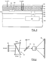
- Figures 9 and 10 show the structure of a reflection type liquid crystal light valve used in conventional projection type liquid crystal display units.
- a pixel array region 4 on which display electrodes consisting of a thin aluminum (Al) film and having functions as a light reflecting film are formed for each pixel, is formed on the silicon substrate 2.
- a counter electrode 16 is provided on the counter substrate such as a glass substrate 14.
- the silicon substrate 2 is bonded face to face to the glass substrate 14 using a sealant 30, and liquid crystals 18 are enclosed in the region between the pixel array region 4 and the counter electrode 16.
- the orientation films to align the liquid crystal molecules 18 is not shown, they are formed on the pixel array region 4 and the counter electrode 16 of the sides contacting the liquid crystals.
- the predetermined cell gap In order to achieve desired electro-optical properties of the liquid crystals, the predetermined cell gap must be maintained uniformly over the entire area of pixel array of the panel.
- some display units use a large number of glass or Resin beads 32 having a diameter of several microns dispersed in the region between the pixel array region 4 and the counter electrode 16 as spacers to make the cell gap even (Fig 9).
- this method of using spacer beads 32 has problems of the uniformity in the diameter of spacer beads 32 and difficulty in the even dispersion of spacer beads 32 on the panel, as well as nonuniform orientation and decrease in brightness and/or optical aperture depending on the location of spacers 32 on pixel array region 4.
- columnar spacers 34 override nearby pixel arrays and form difference in levels (not shown) to decrease the light reflecting area of the Al light reflecting film, reducing the optical aperture of subpixels.
- spacer beads or spacer columns are present in the pixel array region, they disturb the orientation of liquid crystals molecules near the spacers, and become visible when the LCD is activated.
- the disturbance of liquid crystal orientation is enlarged and projected, and becomes more serious with increase in the size of the display screen in higher definition, larger screen projectors. This causes the degradation of display qualities, and must be solved.
- the invention provides a liquid crystal display unit comprising a substrate on which a pixel array region having a plurality of display electrodes are formed, a transparent counter substrate on which a transparent electrode facing to said pixel array region is formed, and spacers formed on the outside immediate to said pixel array region on said substrate and adopted to bond said substrate to said transparent counter substrate maintaining a prescribed cell gap.
- the spacers are formed as a plurality of narrow walls in parallel in the outside immediate to said pixel array region.
- the most external wall of said spacers is also used as sealants for sealing liquid crystals.
- the invention yet further provides a liquid crystal display unit comprising a substrate having a plurality of display electrodes, on which a pixel array region having light shielding regions between said display-electrodes, a transparent counter substrate on which a transparent electrode facing to said pixel array region is formed, and spacers formed in said light shielding regions on said substrate in a width smaller than the width of said light shielding regions, and adopted to bond said substrate to said transparent counter substrate maintaining a prescribed cell gap.
- the spacers are formed of a photo sensitive material having adhesive properties.
- the substrate is a silicon substrate, and said display electrodes are formed of a light reflecting material.
- a reflection type liquid crystal light valve and a method for the manufacture thereof according to an embodiment of the present invention will be described referring to Figures 1-8.
- Figure 1 is a top view of the reflection type liquid crystal light valve according to this embodiment
- Figure 2 is a sectional view along the line A-A of Figure 1.
- the silicon substrate 2 and the glass substrate 14 face to each other, and bonded using narrow wall of spacers 6, 8, 10 and 12 consisting of an adhesive resin formed in parallel outside immediate to the pixel array region 4.
- Liquid crystals 18 are enclosed in the region between the pixel array region 4 and the counter electrode 16. Orientation films (not shown) are formed on the sides contacting the liquid crystals 18 of the pixel array region 4 and the counter electrode 16. No spacers are formed on the pixel array region 4.
- a plurality of liquid crystal inlets 20, 22, 24 and 25 are provided on each of narrow wall of spacers 6-12 formed in parallel outside immediate to the pixel array region 4, a plurality of liquid crystal inlets 20, 22, 24 and 25 are provided.
- a sealant (not shown) is provided by the most external wall of spacers.
- the band spacers 6-12 of this embodiment are adopted to bond the upper and lower substrate in the outside of the pixel array region 4, and also to maintain the gap between the pixel array region 4 and the counter electrode 16 (cell gap) constant.
- a projection type liquid crystal display unit may be provided with enhanced display brightness and improved display qualities by preventing uneven or poor orientation to liquid crystal molecules.
- the silicon substrate 2 used in the reflection type light valve of this embodiment is square with a side A of about 20 to 35 mm, and the pixel array region 4 is a square with a side B of about 15 to 30 mm, on which pixels are formed as a matrix of 1,600 rows by 1,280 columns.
- the thickness D, F and H of the spacers of wall is about 10 ⁇ m, their height I is about 3.2 ⁇ m, the distance between spacers C, E and G is about 10 ⁇ m, and the cell gap J is 3 ⁇ m.
- a transistor 104 of which details are not shown is formed on a silicon substrate 100.
- a silicon oxide film 102 of a thickness of about 2 ⁇ m is formed over the silicon substrate 100 and the transistor 104, and a light absorbing layer 106 is formed over the silicon oxide film 102.
- a silicon nitride film 108 of a thickness of 5,000 ⁇ is formed over the light absorbing layer 106, over which a light reflection layer 112 consisting of Al of a thickness of 1,500 ⁇ is formed.
- the light reflecting layer 112 is connected to the source electrode (not shown) of the transistor 104 by a tungsten (W) stud 110 buried in the through-hole formed through the silicon oxide film 102 and the silicon nitride film 108, and also functions as a display electrode for driving the liquid crystals.
- the subpixel of one display pixel is composed of one light reflecting film 112. No Al layer is formed between adjacent light reflecting films 112 (distance: about 1.7 ⁇ m), forming a black matrix which is the light shielding region not to reflect light.
- a protecting glass substrate 116 is formed as the counter substrate, and a counter electrode 114 is formed on the entire surface of the light reflecting film side of the protecting glass substrate 116.
- a prescribed cell gap is maintained between the light reflecting electrode 112 and the counter electrode 114, and liquid crystals are enclosed between them forming a liquid crystal layer 120.
- the transistor 104 is an FET (field effect transistor) having a source electrode as well as a drain electrode (not shown) connected to the data line, and a gate electrode (not shown) connected to the scanning line, and functions as a switching element for supplying voltage impressed on the data line at the ON state of the gate to the light reflecting film 112 which is the display electrode.
- FET field effect transistor
- the transmissivity of the light By changing the transmissivity of the light by changing the orientation of liquid crystal molecules 122 corresponding to the voltage impressed between the light reflecting film 112 which is the display electrode and the counter electrode 114 when the transistor 104 is ON, the light incident from the protection glass substrate 116 is transmitted to the light reflecting film 112, where the light is reflected and emitted again from the protecting glass substrate 116, or the light in not transmitted, for performing display.
- the orientation films are not shown.
- a linearly polarized light from the light source 42 is reflected by a polarized beam splitter 44 and incident to a colour separation prism 46, where the light is separated into three primary colours, red (R), green (G) and blue (B), and incident to reflection type liquid crystal light valves 48, 50 and 52 for red (R), green (G) and blue (B).
- the light brightness modulated by each reflection type liquid crystal light valve for each subpixel is reflected and is incident to the colour separation prism 46 again, which becomes linearly polarized light 90 degrees shifted from the original polarized light, and is incident to the polarized beam splitter 44.
- the light reflected from reflection type liquid crystal light valves 48, 50 and 52 passes through the polarized beam splitter 44, and is incident to the projection lens 54, enlarged, and projected on the screen 56.
- the reflection type liquid crystal light valve of this embodiment features resin spacers of narrow wall 6 to 12 formed in the outside immediate to the pixel array region 4, and as a rule, other structures may be manufactured by the conventional manufacturing method, the method for forming band spacers 6 to 12 in detail, and the method for forming other structures is not described.
- the material for the spacers of narrow wall 6 to 12 is a resin material having both photosensitivity and adhesiveness.
- the resin material having both photosensitivity and adhesiveness is a mixture of a negative photoresist and a hardening agent in a certain ratio.
- a material in which TPAR N-25 MB (main component) and TPAR-Hardening Agent, both available from Tokyo Ohka are mixed in a ratio of 30.6:6 (see K. Matsui, K. Utsumi, H. Ohkubo and C. Sugitani, "Resin and Flexible Metal Bumps for Chip-On-Glass Technology", 43rd Electronic components and Technology Conference, pp. 205-210, Orlando, Florida, June, 1993).
- a resin having photosensitivity and adhesiveness is used in the Chip-On Glass (COG) technology for directly connecting a driver chip of a liquid crystal display unit with a distance between electrodes of several ten microns to a glass substrate of a liquid crystal display unit wired by a transparent conductive film, and its excellent photosensitivity and adhesiveness are demonstrated.
- COG Chip-On Glass
- photosensitive, adhesive resins are advantageous in that they have various states from a tacky state to a completely cured state depending on conditions of light irradiation and heating.
- the adhesion process may be divided into two steps of precure adhesion, which is a semi-cured state, and postcure, which is a completely cured state, making rework and repair possible.
- precure adhesion which is a semi-cured state
- postcure which is a completely cured state
- a mixed solution of a main component and a hardening agent in a certain ratio (for example, a material in which TPAR N-25 MB (main component) and TPAR-Hardening Agent, both available from Tokyo Ohka, are mixed in a ratio of 30.6:6) is applied to the silicon substrate by spinning at 1,500 rpm to a thickness of 3.0 ⁇ m.
- a hot plate at 90°C for 3 minutes, it is exposed to a dose of 75-150 mJ/cm 2 by mirror projection.
- the silicon substrate is developed by immersion and agitation using a developer (5% triethanolamine) at 25°C for 50 seconds, and patterned to form desired spacers of wall.
- the spacers formed on the silicon substrate is compressed and bonded to the glass substrate under the conditions of 1 kg for 30 minutes.
- post-baking is performed as required on the hot plate at 150°C for 30 minutes , or ultraviolet (UV) irradiation at 2-3 J/cm 2 .
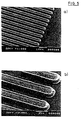
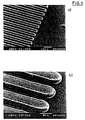
- Narrow wall of spacers formed under the above process conditions are shown in Figure 5 and 6.
- the width of and distance (pitch) between the spacers formed in parallel are 10 ⁇ m, and the thickness of the spacers is 3 ⁇ m.
- the gradient of the walls of the band spacers may be changed.
- Figure 5(a) is a scanning electron micrograph (SEM) of spacers exposed at 75 mJ/cm 2
- Figure 5(b) is an enlarged view of Figure 5(a)
- Figure 6(a) is a scanning electron micrograph (SEM) of spacers exposed at 100 mJ/cm 2
- Figure 6(b) is an enlarged view of Figure 6(a). With increase in exposure dose, the gradient of the wall becomes larger.
- Figures 7(a), (b) and (c) show examples of these spacers formed on a silicon substrate.
- the SEMs of these spacers formed on the silicon substrate, and bonded to the glass counter substrate by compressing and heating are shown in Figure 8. They are enlarged in the order of Figures 8(a), (b) and (c).
- a number of narrow wall of spacers may be formed in parallel outside immediate to the pixel array region 4. Since desired patterns may by formed freely by utilizing photosensitivity, and multiple spacers may be arranged by utilizing adhesiveness, a sufficient mechanical strength is obtained.
- the peel strength of a spacer was 5 MPa (5 kgf/cm 2 ).
- the variation of the cell gap between surfaces was 3 ⁇ m ⁇ 3% (900 ⁇ ), and cell gap of high precision was achieved by avoiding the warping of glass, which depends on the thickness and the total area of the glass.
- the adhesion strength of the spacers may be varied within the range between 0.1 and 1.5 MPa by varying the heating temperature within the range between 50°C and 160°C and by varying the compression pressure within the range between 0.4 kg/cm 2 and 5.5 kg/cm 2 , or by irradiating 2J/cm 2 or more ultraviolet rays.
- the pitch of the spacers for example, was 10 ⁇ m, these values may be changed by changing the mask pattern.
- the cell gap may be controlled in high precision.
- the base material is not limited to an insulator film such as a silicon oxide film, metals, ITO (indium-tin oxide) used as a transparent electrode, or glass may be used, and the thin resin film may be formed either on the array substrate side or on the counter substrate side.
- an insulator film such as a silicon oxide film, metals, ITO (indium-tin oxide) used as a transparent electrode, or glass may be used, and the thin resin film may be formed either on the array substrate side or on the counter substrate side.
- the requirement of width and thickness of micron orders and demand for the process accuracy of one-tenth of the width and thickness may be achieved by the process using the photolithography process, and the requirement of maintaining a sufficient mechanical strength between two substrates of 20-30 mm by 20-30 mm was met by the adhesiveness of the spacers.
- a resin having both photosensitivity and adhesiveness is adopted as the material for forming spacers, and a number of spacers of narrow wall are arranged in parallel outside of the pixel array region.
- the present invention is applied to a reflection type liquid crystal light valve of Si-LCD used in projection type liquid crystal display unit in the above embodiment, the present invention may be applied to other type of liquid crystal display units, such as transmission type liquid crystal light valves, or liquid crystal display units in which pixel regions are formed on a glass substrate.
- the spacers having a smaller width than the width of the black matrix may be formed on the region of the black matrix in the pixel array region 4. In this case, although the effect of the above embodiment is reduced, the display qualities are still improved over conventional spacers.
- a liquid crystal display unit with the improved accuracy and uniformity between substrate surfaces of the cell gap is provided.
- the cell gap may easily be controlled.
Landscapes
- Physics & Mathematics (AREA)
- Nonlinear Science (AREA)
- Mathematical Physics (AREA)
- Chemical & Material Sciences (AREA)
- Crystallography & Structural Chemistry (AREA)
- General Physics & Mathematics (AREA)
- Optics & Photonics (AREA)
- Liquid Crystal (AREA)
- Overhead Projectors And Projection Screens (AREA)
Applications Claiming Priority (3)
| Application Number | Priority Date | Filing Date | Title |
|---|---|---|---|
| JP125863/95 | 1995-04-26 | ||
| JP7125863A JPH08297286A (ja) | 1995-04-26 | 1995-04-26 | 液晶表示装置 |
| US08/666,682 US5777713A (en) | 1995-04-26 | 1996-06-17 | Liquid crystal display unit with spacers form in the light shielding regions |
Publications (2)
| Publication Number | Publication Date |
|---|---|
| EP0740186A2 true EP0740186A2 (fr) | 1996-10-30 |
| EP0740186A3 EP0740186A3 (fr) | 1997-04-23 |
Family
ID=26462167
Family Applications (1)
| Application Number | Title | Priority Date | Filing Date |
|---|---|---|---|
| EP96301357A Withdrawn EP0740186A3 (fr) | 1995-04-26 | 1996-02-28 | Unité d'affichage à cristal liquide |
Country Status (3)
| Country | Link |
|---|---|
| US (1) | US5777713A (fr) |
| EP (1) | EP0740186A3 (fr) |
| JP (1) | JPH08297286A (fr) |
Cited By (7)
| Publication number | Priority date | Publication date | Assignee | Title |
|---|---|---|---|---|
| WO2001011423A1 (fr) * | 1999-08-05 | 2001-02-15 | Koninklijke Philips Electronics N.V. | Entretoise pour ecran a cristaux liquides |
| EP1076257A3 (fr) * | 1999-08-13 | 2001-07-11 | International Business Machines Corporation | Dispositif d'affichage à cristal liquide et son procédé de fabrication |
| EP1502902A1 (fr) * | 2003-07-30 | 2005-02-02 | Glaverbel | Panneau de verre |
| WO2005012202A1 (fr) * | 2003-07-30 | 2005-02-10 | Glaverbel | Panneau de vitrage |
| EP1357419A4 (fr) * | 2001-02-02 | 2006-11-29 | Citizen Watch Co Ltd | Obturateur a cristaux liquides pour systeme d'exposition |
| CN100428028C (zh) * | 2007-01-04 | 2008-10-22 | 北京京东方光电科技有限公司 | 一种液晶显示器面板 |
| US8854593B2 (en) | 1997-05-22 | 2014-10-07 | Semiconductor Energy Laboratory Co., Ltd. | Electro-optical device |
Families Citing this family (54)
| Publication number | Priority date | Publication date | Assignee | Title |
|---|---|---|---|---|
| DE69530425T2 (de) * | 1995-05-29 | 2003-12-18 | International Business Machines Corp., Armonk | Flüssigkristallanzeige und herstellungsverfahren dafür |
| US6888608B2 (en) * | 1995-09-06 | 2005-05-03 | Kabushiki Kaisha Toshiba | Liquid crystal display device |
| TW373098B (en) | 1995-09-06 | 1999-11-01 | Toshiba Corp | Liquid crystal exposure component and its fabricating method |
| GB2347006B (en) * | 1996-07-26 | 2000-10-04 | Sharp Kk | Liquid crystal device |
| JP4362882B2 (ja) * | 1999-01-13 | 2009-11-11 | ソニー株式会社 | 液晶パネル、液晶パネルの製造方法および液晶表示装置 |
| US6498635B1 (en) * | 1999-03-05 | 2002-12-24 | Chartered Semiconductor Manufacturing Ltd. | Method of forming insulating material alignment posts associated with active device structures |
| US6747727B2 (en) | 1999-04-26 | 2004-06-08 | Hong-Da Liu | Method for the manufacture of a liquid crystal display |
| JP4298131B2 (ja) * | 1999-05-14 | 2009-07-15 | 株式会社半導体エネルギー研究所 | 液晶表示装置の作製方法 |
| US6680487B1 (en) * | 1999-05-14 | 2004-01-20 | Semiconductor Energy Laboratory Co., Ltd. | Semiconductor comprising a TFT provided on a substrate having an insulating surface and method of fabricating the same |
| US6630977B1 (en) * | 1999-05-20 | 2003-10-07 | Semiconductor Energy Laboratory Co., Ltd. | Semiconductor device with capacitor formed around contact hole |
| TW459275B (en) | 1999-07-06 | 2001-10-11 | Semiconductor Energy Lab | Semiconductor device and method of fabricating the same |
| US7071041B2 (en) * | 2000-01-20 | 2006-07-04 | Semiconductor Energy Laboratory Co., Ltd. | Method of manufacturing a semiconductor device |
| JP2001305561A (ja) * | 2000-04-21 | 2001-10-31 | Hitachi Ltd | 液晶表示装置 |
| US6747724B2 (en) * | 2000-07-26 | 2004-06-08 | Casio Computer Co., Ltd. | Liquid crystal display device having non-display area with reduced width |
| US6819391B2 (en) * | 2001-11-30 | 2004-11-16 | Lg. Philips Lcd Co., Ltd. | Liquid crystal display panel having dummy column spacer with opened portion |
| KR100685948B1 (ko) * | 2001-12-14 | 2007-02-23 | 엘지.필립스 엘시디 주식회사 | 액정표시소자 및 그 제조방법 |
| KR20030058726A (ko) * | 2001-12-31 | 2003-07-07 | 비오이 하이디스 테크놀로지 주식회사 | 평판표시소자의 기판 합착방법 |
| US7408598B2 (en) * | 2002-02-20 | 2008-08-05 | Planar Systems, Inc. | Light sensitive display with selected interval of light sensitive elements |
| US7053967B2 (en) | 2002-05-23 | 2006-05-30 | Planar Systems, Inc. | Light sensitive display |
| US7009663B2 (en) | 2003-12-17 | 2006-03-07 | Planar Systems, Inc. | Integrated optical light sensitive active matrix liquid crystal display |
| WO2003075207A2 (fr) * | 2002-03-01 | 2003-09-12 | Planar Systems, Inc. | Ecrans tactiles antireflets |
| US7179512B2 (en) | 2002-05-14 | 2007-02-20 | Fujitsu Limited | Liquid crystal display and manufacturing method of same |
| JP4059735B2 (ja) | 2002-09-03 | 2008-03-12 | 株式会社 日立ディスプレイズ | 液晶表示装置 |
| US20080084374A1 (en) | 2003-02-20 | 2008-04-10 | Planar Systems, Inc. | Light sensitive display |
| TWI306530B (en) * | 2003-10-01 | 2009-02-21 | Himax Tech Inc | Liquid crystal display panel and liquid crystal on silicon display panel |
| US20050134749A1 (en) * | 2003-12-19 | 2005-06-23 | Adiel Abileah | Reflection resistant display |
| US7773139B2 (en) | 2004-04-16 | 2010-08-10 | Apple Inc. | Image sensor with photosensitive thin film transistors |
| KR101080401B1 (ko) * | 2004-04-23 | 2011-11-04 | 삼성전자주식회사 | 평판 표시장치의 접합구조체 및 그 형성방법과 이를구비하는 평판 표시장치 |
| US20060045240A1 (en) * | 2004-08-31 | 2006-03-02 | Buchner Gregory C | Method and apparatus for delayed answering of telecommunications request |
| KR20060110936A (ko) * | 2005-04-20 | 2006-10-26 | 엘지.필립스 엘시디 주식회사 | 액정 표시 장치 및 이의 제조 방법 |
| KR100814819B1 (ko) * | 2006-10-31 | 2008-03-20 | 삼성에스디아이 주식회사 | 플라즈마 디스플레이 장치 |
| US20080251976A1 (en) * | 2007-04-13 | 2008-10-16 | Liquidia Technologies, Inc. | Micro and nano-spacers having highly uniform size and shape |
| JP5428152B2 (ja) * | 2007-12-04 | 2014-02-26 | 日立化成株式会社 | 接続構造体の製造方法 |
| CN102135687B (zh) * | 2009-11-03 | 2013-07-10 | 深超光电(深圳)有限公司 | 显示面板 |
| US9310923B2 (en) | 2010-12-03 | 2016-04-12 | Apple Inc. | Input device for touch sensitive devices |
| US9329703B2 (en) | 2011-06-22 | 2016-05-03 | Apple Inc. | Intelligent stylus |
| US8928635B2 (en) | 2011-06-22 | 2015-01-06 | Apple Inc. | Active stylus |
| US8638320B2 (en) | 2011-06-22 | 2014-01-28 | Apple Inc. | Stylus orientation detection |
| US9176604B2 (en) | 2012-07-27 | 2015-11-03 | Apple Inc. | Stylus device |
| US9557845B2 (en) | 2012-07-27 | 2017-01-31 | Apple Inc. | Input device for and method of communication with capacitive devices through frequency variation |
| US9652090B2 (en) | 2012-07-27 | 2017-05-16 | Apple Inc. | Device for digital communication through capacitive coupling |
| JP2013137568A (ja) * | 2013-02-27 | 2013-07-11 | Semiconductor Energy Lab Co Ltd | 液晶表示装置 |
| US10048775B2 (en) | 2013-03-14 | 2018-08-14 | Apple Inc. | Stylus detection and demodulation |
| US9762868B2 (en) | 2013-06-28 | 2017-09-12 | Thomson Licensing | Highlighting an object displayed by a pico projector |
| US10845901B2 (en) | 2013-07-31 | 2020-11-24 | Apple Inc. | Touch controller architecture |
| JP2014059583A (ja) * | 2013-12-05 | 2014-04-03 | Semiconductor Energy Lab Co Ltd | 表示装置 |
| US10061449B2 (en) | 2014-12-04 | 2018-08-28 | Apple Inc. | Coarse scan and targeted active mode scan for touch and stylus |
| CN204389840U (zh) * | 2015-01-04 | 2015-06-10 | 京东方科技集团股份有限公司 | 一种基板及光电显示装置 |
| JP6039745B2 (ja) * | 2015-05-25 | 2016-12-07 | 株式会社半導体エネルギー研究所 | 表示装置 |
| US10474277B2 (en) | 2016-05-31 | 2019-11-12 | Apple Inc. | Position-based stylus communication |
| CN105892166B (zh) * | 2016-06-29 | 2019-08-13 | 厦门天马微电子有限公司 | 一种液晶显示装置及电子设备 |
| CN206479739U (zh) * | 2017-03-03 | 2017-09-08 | 京东方科技集团股份有限公司 | 一种显示面板以及显示设备 |
| WO2022064999A1 (fr) * | 2020-09-25 | 2022-03-31 | ソニーセミコンダクタソリューションズ株式会社 | Dispositif d'affichage à cristaux liquides et dispositif d'affichage par projection |
| US12153764B1 (en) | 2020-09-25 | 2024-11-26 | Apple Inc. | Stylus with receive architecture for position determination |
Citations (1)
| Publication number | Priority date | Publication date | Assignee | Title |
|---|---|---|---|---|
| JPH01257824A (ja) * | 1988-04-07 | 1989-10-13 | Toppan Printing Co Ltd | 液晶パネルの製造方法 |
Family Cites Families (5)
| Publication number | Priority date | Publication date | Assignee | Title |
|---|---|---|---|---|
| JPS57171319A (en) * | 1981-04-15 | 1982-10-21 | Hitachi Ltd | Liquid crystal display element |
| CH676888A5 (fr) * | 1988-09-07 | 1991-03-15 | Asulab Sa | |
| FR2693005B1 (fr) * | 1992-06-26 | 1995-03-31 | Thomson Lcd | Disposition d'encapsulation et de passivation de circuit pour écrans plats. |
| US5556670A (en) * | 1992-10-15 | 1996-09-17 | Casio Computer Co., Ltd. | Liquid crystal display panel |
| US5517344A (en) * | 1994-05-20 | 1996-05-14 | Prime View Hk Limited | System for protection of drive circuits formed on a substrate of a liquid crystal display |
-
1995
- 1995-04-26 JP JP7125863A patent/JPH08297286A/ja active Pending
-
1996
- 1996-02-28 EP EP96301357A patent/EP0740186A3/fr not_active Withdrawn
- 1996-06-17 US US08/666,682 patent/US5777713A/en not_active Expired - Lifetime
Patent Citations (1)
| Publication number | Priority date | Publication date | Assignee | Title |
|---|---|---|---|---|
| JPH01257824A (ja) * | 1988-04-07 | 1989-10-13 | Toppan Printing Co Ltd | 液晶パネルの製造方法 |
Cited By (9)
| Publication number | Priority date | Publication date | Assignee | Title |
|---|---|---|---|---|
| US8854593B2 (en) | 1997-05-22 | 2014-10-07 | Semiconductor Energy Laboratory Co., Ltd. | Electro-optical device |
| WO2001011423A1 (fr) * | 1999-08-05 | 2001-02-15 | Koninklijke Philips Electronics N.V. | Entretoise pour ecran a cristaux liquides |
| EP1076257A3 (fr) * | 1999-08-13 | 2001-07-11 | International Business Machines Corporation | Dispositif d'affichage à cristal liquide et son procédé de fabrication |
| US7088418B1 (en) | 1999-08-13 | 2006-08-08 | International Business Machines Corporation | Liquid crystal display device and method of fabricating the same |
| EP1357419A4 (fr) * | 2001-02-02 | 2006-11-29 | Citizen Watch Co Ltd | Obturateur a cristaux liquides pour systeme d'exposition |
| EP1502902A1 (fr) * | 2003-07-30 | 2005-02-02 | Glaverbel | Panneau de verre |
| WO2005012202A1 (fr) * | 2003-07-30 | 2005-02-10 | Glaverbel | Panneau de vitrage |
| US7833592B2 (en) | 2003-07-30 | 2010-11-16 | Agc Glass Europe | Glazing panel |
| CN100428028C (zh) * | 2007-01-04 | 2008-10-22 | 北京京东方光电科技有限公司 | 一种液晶显示器面板 |
Also Published As
| Publication number | Publication date |
|---|---|
| JPH08297286A (ja) | 1996-11-12 |
| EP0740186A3 (fr) | 1997-04-23 |
| US5777713A (en) | 1998-07-07 |
Similar Documents
| Publication | Publication Date | Title |
|---|---|---|
| US5777713A (en) | Liquid crystal display unit with spacers form in the light shielding regions | |
| US7738073B2 (en) | Liquid crystal display and method of fabricating the same | |
| US6373547B2 (en) | Liquid crystal display device having pole spacers formed over optical shield film | |
| US6636192B1 (en) | Electrooptic panel, projection display, and method for manufacturing electrooptic panel | |
| US7456926B2 (en) | Liquid crystal display device | |
| US6642992B2 (en) | Liquid crystal display panel and method of manufacturing the same | |
| US20120229736A1 (en) | Liquid crystal panel and liquid crystal display device | |
| EP1681592A1 (fr) | Substrat comprenant un element d'ecartement, panneau, panneau a cristaux liquides, procede de production de panneau et procede de production de panneau a cristaux liquides | |
| KR20080040051A (ko) | 마이크로 렌즈 어레이가 제공된 표시 패널의 제조 방법,표시 장치 및 노광장치 | |
| JP3483730B2 (ja) | 液晶表示装置 | |
| JP4315084B2 (ja) | マイクロレンズアレイ板及びその製造方法、並びにこれを備えた電気光学装置及び電子機器 | |
| JP2007041625A (ja) | 液晶表示装置及びその製造方法 | |
| KR100242481B1 (ko) | 액정 표시 장치 | |
| US20090109382A1 (en) | Substrate for liquid crystal display device and liquid crystal display device including the same | |
| JP7760514B2 (ja) | 液晶表示装置および投射型表示装置 | |
| JP3697945B2 (ja) | 電気光学装置の製造方法 | |
| JP2006267158A (ja) | マイクロレンズ基板及びその製造方法、電気光学装置及びその製造方法、並びに電子機器 | |
| US20040156007A1 (en) | Substrate for liquid crystal display and liquid crystal display having the same | |
| JP2005182086A (ja) | 電気光学装置の製造方法 | |
| JP2001201752A (ja) | 電気光学パネル、投射型表示装置、および電気光学パネルの製造方法 | |
| JP2006330142A (ja) | マイクロレンズ基板の製造方法、電気光学装置の製造方法、及びマイクロレンズ基板、並びに電気光学装置及び電子機器 | |
| JP2000206516A (ja) | 液晶プロジェクション装置用マイクロレンズ基板 | |
| JPH10161101A (ja) | 液晶表示素子、その製造方法、及び液晶プロジェクター |
Legal Events
| Date | Code | Title | Description |
|---|---|---|---|
| PUAI | Public reference made under article 153(3) epc to a published international application that has entered the european phase |
Free format text: ORIGINAL CODE: 0009012 |
|
| AK | Designated contracting states |
Kind code of ref document: A2 Designated state(s): DE FR GB |
|
| PUAL | Search report despatched |
Free format text: ORIGINAL CODE: 0009013 |
|
| 17P | Request for examination filed |
Effective date: 19970213 |
|
| AK | Designated contracting states |
Kind code of ref document: A3 Designated state(s): DE FR GB |
|
| 17Q | First examination report despatched |
Effective date: 19980330 |
|
| STAA | Information on the status of an ep patent application or granted ep patent |
Free format text: STATUS: THE APPLICATION IS DEEMED TO BE WITHDRAWN |
|
| 18D | Application deemed to be withdrawn |
Effective date: 20010217 |