EP0740221A1 - Appareil de formation d'images et élément de transfert intermédiaire - Google Patents
Appareil de formation d'images et élément de transfert intermédiaire Download PDFInfo
- Publication number
- EP0740221A1 EP0740221A1 EP96302912A EP96302912A EP0740221A1 EP 0740221 A1 EP0740221 A1 EP 0740221A1 EP 96302912 A EP96302912 A EP 96302912A EP 96302912 A EP96302912 A EP 96302912A EP 0740221 A1 EP0740221 A1 EP 0740221A1
- Authority
- EP
- European Patent Office
- Prior art keywords
- intermediate transfer
- transfer member
- image
- reflectance
- pattern
- Prior art date
- Legal status (The legal status is an assumption and is not a legal conclusion. Google has not performed a legal analysis and makes no representation as to the accuracy of the status listed.)
- Granted
Links
- 238000012546 transfer Methods 0.000 title claims abstract description 151
- 238000001514 detection method Methods 0.000 claims abstract description 24
- 239000010410 layer Substances 0.000 claims description 27
- 239000002344 surface layer Substances 0.000 claims description 21
- 239000000049 pigment Substances 0.000 claims description 16
- GWEVSGVZZGPLCZ-UHFFFAOYSA-N Titan oxide Chemical compound O=[Ti]=O GWEVSGVZZGPLCZ-UHFFFAOYSA-N 0.000 claims description 11
- 239000011247 coating layer Substances 0.000 claims description 10
- 235000010215 titanium dioxide Nutrition 0.000 claims description 6
- 239000000314 lubricant Substances 0.000 claims 1
- 239000012463 white pigment Substances 0.000 claims 1
- 229920005989 resin Polymers 0.000 description 22
- 239000011347 resin Substances 0.000 description 22
- 229920001577 copolymer Polymers 0.000 description 18
- 230000003595 spectral effect Effects 0.000 description 17
- 229920001971 elastomer Polymers 0.000 description 14
- 239000003973 paint Substances 0.000 description 13
- 150000001875 compounds Chemical class 0.000 description 11
- XLOMVQKBTHCTTD-UHFFFAOYSA-N Zinc monoxide Chemical compound [Zn]=O XLOMVQKBTHCTTD-UHFFFAOYSA-N 0.000 description 10
- 238000001739 density measurement Methods 0.000 description 10
- 239000003086 colorant Substances 0.000 description 9
- 238000000034 method Methods 0.000 description 9
- YXIWHUQXZSMYRE-UHFFFAOYSA-N 1,3-benzothiazole-2-thiol Chemical compound C1=CC=C2SC(S)=NC2=C1 YXIWHUQXZSMYRE-UHFFFAOYSA-N 0.000 description 8
- -1 polyethylene Polymers 0.000 description 8
- 239000005060 rubber Substances 0.000 description 8
- YXFVVABEGXRONW-UHFFFAOYSA-N Toluene Chemical compound CC1=CC=CC=C1 YXFVVABEGXRONW-UHFFFAOYSA-N 0.000 description 6
- 239000000806 elastomer Substances 0.000 description 6
- 239000000463 material Substances 0.000 description 6
- 235000014692 zinc oxide Nutrition 0.000 description 6
- 239000011787 zinc oxide Substances 0.000 description 6
- PPBRXRYQALVLMV-UHFFFAOYSA-N Styrene Chemical compound C=CC1=CC=CC=C1 PPBRXRYQALVLMV-UHFFFAOYSA-N 0.000 description 5
- 230000000052 comparative effect Effects 0.000 description 5
- 238000011156 evaluation Methods 0.000 description 5
- 239000002245 particle Substances 0.000 description 5
- 229920001343 polytetrafluoroethylene Polymers 0.000 description 5
- 239000004810 polytetrafluoroethylene Substances 0.000 description 5
- 238000002360 preparation method Methods 0.000 description 5
- OGIDPMRJRNCKJF-UHFFFAOYSA-N titanium oxide Inorganic materials [Ti]=O OGIDPMRJRNCKJF-UHFFFAOYSA-N 0.000 description 5
- 239000006229 carbon black Substances 0.000 description 4
- 238000004073 vulcanization Methods 0.000 description 4
- 229920001730 Moisture cure polyurethane Polymers 0.000 description 3
- 239000004698 Polyethylene Substances 0.000 description 3
- 239000004743 Polypropylene Substances 0.000 description 3
- XUIMIQQOPSSXEZ-UHFFFAOYSA-N Silicon Chemical compound [Si] XUIMIQQOPSSXEZ-UHFFFAOYSA-N 0.000 description 3
- NINIDFKCEFEMDL-UHFFFAOYSA-N Sulfur Chemical compound [S] NINIDFKCEFEMDL-UHFFFAOYSA-N 0.000 description 3
- 229910052782 aluminium Inorganic materials 0.000 description 3
- XAGFODPZIPBFFR-UHFFFAOYSA-N aluminium Chemical compound [Al] XAGFODPZIPBFFR-UHFFFAOYSA-N 0.000 description 3
- 239000011324 bead Substances 0.000 description 3
- 230000008859 change Effects 0.000 description 3
- 239000003795 chemical substances by application Substances 0.000 description 3
- 238000001816 cooling Methods 0.000 description 3
- 239000006185 dispersion Substances 0.000 description 3
- 230000003287 optical effect Effects 0.000 description 3
- 229920000573 polyethylene Polymers 0.000 description 3
- 229920001155 polypropylene Polymers 0.000 description 3
- 229910052710 silicon Inorganic materials 0.000 description 3
- 239000010703 silicon Substances 0.000 description 3
- 229920002379 silicone rubber Polymers 0.000 description 3
- 229920003048 styrene butadiene rubber Polymers 0.000 description 3
- 239000000126 substance Substances 0.000 description 3
- 229910052717 sulfur Inorganic materials 0.000 description 3
- 239000011593 sulfur Substances 0.000 description 3
- KUAZQDVKQLNFPE-UHFFFAOYSA-N thiram Chemical compound CN(C)C(=S)SSC(=S)N(C)C KUAZQDVKQLNFPE-UHFFFAOYSA-N 0.000 description 3
- 229960002447 thiram Drugs 0.000 description 3
- PEVRKKOYEFPFMN-UHFFFAOYSA-N 1,1,2,3,3,3-hexafluoroprop-1-ene;1,1,2,2-tetrafluoroethene Chemical group FC(F)=C(F)F.FC(F)=C(F)C(F)(F)F PEVRKKOYEFPFMN-UHFFFAOYSA-N 0.000 description 2
- KXGFMDJXCMQABM-UHFFFAOYSA-N 2-methoxy-6-methylphenol Chemical compound [CH]OC1=CC=CC([CH])=C1O KXGFMDJXCMQABM-UHFFFAOYSA-N 0.000 description 2
- OKTJSMMVPCPJKN-UHFFFAOYSA-N Carbon Chemical compound [C] OKTJSMMVPCPJKN-UHFFFAOYSA-N 0.000 description 2
- XEEYBQQBJWHFJM-UHFFFAOYSA-N Iron Chemical compound [Fe] XEEYBQQBJWHFJM-UHFFFAOYSA-N 0.000 description 2
- PXHVJJICTQNCMI-UHFFFAOYSA-N Nickel Chemical compound [Ni] PXHVJJICTQNCMI-UHFFFAOYSA-N 0.000 description 2
- 229920000459 Nitrile rubber Polymers 0.000 description 2
- 239000005662 Paraffin oil Substances 0.000 description 2
- 239000004793 Polystyrene Substances 0.000 description 2
- VYPSYNLAJGMNEJ-UHFFFAOYSA-N Silicium dioxide Chemical compound O=[Si]=O VYPSYNLAJGMNEJ-UHFFFAOYSA-N 0.000 description 2
- TZCXTZWJZNENPQ-UHFFFAOYSA-L barium sulfate Chemical compound [Ba+2].[O-]S([O-])(=O)=O TZCXTZWJZNENPQ-UHFFFAOYSA-L 0.000 description 2
- 229910052799 carbon Inorganic materials 0.000 description 2
- 238000004140 cleaning Methods 0.000 description 2
- 229920006026 co-polymeric resin Polymers 0.000 description 2
- 238000004040 coloring Methods 0.000 description 2
- 238000003475 lamination Methods 0.000 description 2
- 230000001050 lubricating effect Effects 0.000 description 2
- 229910052751 metal Inorganic materials 0.000 description 2
- 239000002184 metal Substances 0.000 description 2
- 230000002093 peripheral effect Effects 0.000 description 2
- 229920001568 phenolic resin Polymers 0.000 description 2
- 239000005011 phenolic resin Substances 0.000 description 2
- 229920000642 polymer Polymers 0.000 description 2
- 230000008569 process Effects 0.000 description 2
- 230000005855 radiation Effects 0.000 description 2
- 229920002050 silicone resin Polymers 0.000 description 2
- 239000004945 silicone rubber Substances 0.000 description 2
- 238000005507 spraying Methods 0.000 description 2
- BFKJFAAPBSQJPD-UHFFFAOYSA-N tetrafluoroethene Chemical group FC(F)=C(F)F BFKJFAAPBSQJPD-UHFFFAOYSA-N 0.000 description 2
- BQCIDUSAKPWEOX-UHFFFAOYSA-N 1,1-Difluoroethene Chemical compound FC(F)=C BQCIDUSAKPWEOX-UHFFFAOYSA-N 0.000 description 1
- UPVJEODAZWTJKZ-UHFFFAOYSA-N 1,2-dichloro-1,2-difluoroethene Chemical group FC(Cl)=C(F)Cl UPVJEODAZWTJKZ-UHFFFAOYSA-N 0.000 description 1
- 239000004925 Acrylic resin Substances 0.000 description 1
- 229920000178 Acrylic resin Polymers 0.000 description 1
- ZOXJGFHDIHLPTG-UHFFFAOYSA-N Boron Chemical compound [B] ZOXJGFHDIHLPTG-UHFFFAOYSA-N 0.000 description 1
- RYGMFSIKBFXOCR-UHFFFAOYSA-N Copper Chemical compound [Cu] RYGMFSIKBFXOCR-UHFFFAOYSA-N 0.000 description 1
- YCKRFDGAMUMZLT-UHFFFAOYSA-N Fluorine atom Chemical compound [F] YCKRFDGAMUMZLT-UHFFFAOYSA-N 0.000 description 1
- UFWIBTONFRDIAS-UHFFFAOYSA-N Naphthalene Chemical compound C1=CC=CC2=CC=CC=C21 UFWIBTONFRDIAS-UHFFFAOYSA-N 0.000 description 1
- 239000004677 Nylon Substances 0.000 description 1
- CTQNGGLPUBDAKN-UHFFFAOYSA-N O-Xylene Chemical compound CC1=CC=CC=C1C CTQNGGLPUBDAKN-UHFFFAOYSA-N 0.000 description 1
- 239000005062 Polybutadiene Substances 0.000 description 1
- 229920002873 Polyethylenimine Polymers 0.000 description 1
- 235000021355 Stearic acid Nutrition 0.000 description 1
- 229920007962 Styrene Methyl Methacrylate Polymers 0.000 description 1
- 239000002174 Styrene-butadiene Substances 0.000 description 1
- 229920006311 Urethane elastomer Polymers 0.000 description 1
- BZHJMEDXRYGGRV-UHFFFAOYSA-N Vinyl chloride Chemical compound ClC=C BZHJMEDXRYGGRV-UHFFFAOYSA-N 0.000 description 1
- 238000005299 abrasion Methods 0.000 description 1
- 229920000800 acrylic rubber Polymers 0.000 description 1
- 230000009471 action Effects 0.000 description 1
- 229910045601 alloy Inorganic materials 0.000 description 1
- 239000000956 alloy Substances 0.000 description 1
- XYLMUPLGERFSHI-UHFFFAOYSA-N alpha-Methylstyrene Chemical compound CC(=C)C1=CC=CC=C1 XYLMUPLGERFSHI-UHFFFAOYSA-N 0.000 description 1
- PNEYBMLMFCGWSK-UHFFFAOYSA-N aluminium oxide Inorganic materials [O-2].[O-2].[O-2].[Al+3].[Al+3] PNEYBMLMFCGWSK-UHFFFAOYSA-N 0.000 description 1
- OJMOMXZKOWKUTA-UHFFFAOYSA-N aluminum;borate Chemical compound [Al+3].[O-]B([O-])[O-] OJMOMXZKOWKUTA-UHFFFAOYSA-N 0.000 description 1
- 229910052796 boron Inorganic materials 0.000 description 1
- 229920005549 butyl rubber Polymers 0.000 description 1
- UUAGAQFQZIEFAH-UHFFFAOYSA-N chlorotrifluoroethylene Chemical group FC(F)=C(F)Cl UUAGAQFQZIEFAH-UHFFFAOYSA-N 0.000 description 1
- 229910052802 copper Inorganic materials 0.000 description 1
- 239000010949 copper Substances 0.000 description 1
- XCJYREBRNVKWGJ-UHFFFAOYSA-N copper(II) phthalocyanine Chemical compound [Cu+2].C12=CC=CC=C2C(N=C2[N-]C(C3=CC=CC=C32)=N2)=NC1=NC([C]1C=CC=CC1=1)=NC=1N=C1[C]3C=CC=CC3=C2[N-]1 XCJYREBRNVKWGJ-UHFFFAOYSA-N 0.000 description 1
- 230000006866 deterioration Effects 0.000 description 1
- 125000000664 diazo group Chemical group [N-]=[N+]=[*] 0.000 description 1
- 235000014113 dietary fatty acids Nutrition 0.000 description 1
- REQPQFUJGGOFQL-UHFFFAOYSA-N dimethylcarbamothioyl n,n-dimethylcarbamodithioate Chemical compound CN(C)C(=S)SC(=S)N(C)C REQPQFUJGGOFQL-UHFFFAOYSA-N 0.000 description 1
- 230000000694 effects Effects 0.000 description 1
- 230000005684 electric field Effects 0.000 description 1
- 229920005558 epichlorohydrin rubber Polymers 0.000 description 1
- 239000003822 epoxy resin Substances 0.000 description 1
- 229920006244 ethylene-ethyl acrylate Polymers 0.000 description 1
- 239000000194 fatty acid Substances 0.000 description 1
- 229930195729 fatty acid Natural products 0.000 description 1
- 150000004665 fatty acids Chemical class 0.000 description 1
- 239000000945 filler Substances 0.000 description 1
- 239000011737 fluorine Substances 0.000 description 1
- 229910052731 fluorine Inorganic materials 0.000 description 1
- XUCNUKMRBVNAPB-UHFFFAOYSA-N fluoroethene Chemical compound FC=C XUCNUKMRBVNAPB-UHFFFAOYSA-N 0.000 description 1
- 229920001519 homopolymer Polymers 0.000 description 1
- 238000005286 illumination Methods 0.000 description 1
- 229910003437 indium oxide Inorganic materials 0.000 description 1
- PJXISJQVUVHSOJ-UHFFFAOYSA-N indium(iii) oxide Chemical compound [O-2].[O-2].[O-2].[In+3].[In+3] PJXISJQVUVHSOJ-UHFFFAOYSA-N 0.000 description 1
- 229920000554 ionomer Polymers 0.000 description 1
- 229910052742 iron Inorganic materials 0.000 description 1
- 229920003049 isoprene rubber Polymers 0.000 description 1
- 150000002576 ketones Chemical class 0.000 description 1
- 150000002689 maleic acids Chemical class 0.000 description 1
- 238000004519 manufacturing process Methods 0.000 description 1
- 238000005259 measurement Methods 0.000 description 1
- 229910044991 metal oxide Inorganic materials 0.000 description 1
- 150000004706 metal oxides Chemical class 0.000 description 1
- 239000002923 metal particle Substances 0.000 description 1
- 150000002739 metals Chemical class 0.000 description 1
- QLOAVXSYZAJECW-UHFFFAOYSA-N methane;molecular fluorine Chemical compound C.FF QLOAVXSYZAJECW-UHFFFAOYSA-N 0.000 description 1
- ADFPJHOAARPYLP-UHFFFAOYSA-N methyl 2-methylprop-2-enoate;styrene Chemical compound COC(=O)C(C)=C.C=CC1=CC=CC=C1 ADFPJHOAARPYLP-UHFFFAOYSA-N 0.000 description 1
- 239000000203 mixture Substances 0.000 description 1
- 229910052759 nickel Inorganic materials 0.000 description 1
- JFNLZVQOOSMTJK-KNVOCYPGSA-N norbornene Chemical compound C1[C@@H]2CC[C@H]1C=C2 JFNLZVQOOSMTJK-KNVOCYPGSA-N 0.000 description 1
- 229920001778 nylon Polymers 0.000 description 1
- QIQXTHQIDYTFRH-UHFFFAOYSA-N octadecanoic acid Chemical compound CCCCCCCCCCCCCCCCCC(O)=O QIQXTHQIDYTFRH-UHFFFAOYSA-N 0.000 description 1
- OQCDKBAXFALNLD-UHFFFAOYSA-N octadecanoic acid Natural products CCCCCCCC(C)CCCCCCCCC(O)=O OQCDKBAXFALNLD-UHFFFAOYSA-N 0.000 description 1
- 239000004014 plasticizer Substances 0.000 description 1
- 229920001084 poly(chloroprene) Polymers 0.000 description 1
- 229920003229 poly(methyl methacrylate) Polymers 0.000 description 1
- 229920002037 poly(vinyl butyral) polymer Polymers 0.000 description 1
- 229920000058 polyacrylate Polymers 0.000 description 1
- 229920002857 polybutadiene Polymers 0.000 description 1
- 229920000015 polydiacetylene Polymers 0.000 description 1
- 229920000647 polyepoxide Polymers 0.000 description 1
- 229920001225 polyester resin Polymers 0.000 description 1
- 239000004645 polyester resin Substances 0.000 description 1
- 239000004926 polymethyl methacrylate Substances 0.000 description 1
- 229920000128 polypyrrole Polymers 0.000 description 1
- 229920002223 polystyrene Polymers 0.000 description 1
- 229920005749 polyurethane resin Polymers 0.000 description 1
- 239000010734 process oil Substances 0.000 description 1
- 238000012545 processing Methods 0.000 description 1
- 150000003242 quaternary ammonium salts Chemical class 0.000 description 1
- 239000001054 red pigment Substances 0.000 description 1
- 230000007261 regionalization Effects 0.000 description 1
- 230000003252 repetitive effect Effects 0.000 description 1
- 230000004044 response Effects 0.000 description 1
- 238000000926 separation method Methods 0.000 description 1
- 239000000377 silicon dioxide Substances 0.000 description 1
- 239000010935 stainless steel Substances 0.000 description 1
- 229910001220 stainless steel Inorganic materials 0.000 description 1
- 239000008117 stearic acid Substances 0.000 description 1
- 150000003440 styrenes Chemical class 0.000 description 1
- XOLBLPGZBRYERU-UHFFFAOYSA-N tin dioxide Chemical compound O=[Sn]=O XOLBLPGZBRYERU-UHFFFAOYSA-N 0.000 description 1
- 229910001887 tin oxide Inorganic materials 0.000 description 1
- 238000002834 transmittance Methods 0.000 description 1
- 239000008096 xylene Substances 0.000 description 1
- 239000001052 yellow pigment Substances 0.000 description 1
- DUBNHZYBDBBJHD-UHFFFAOYSA-L ziram Chemical compound [Zn+2].CN(C)C([S-])=S.CN(C)C([S-])=S DUBNHZYBDBBJHD-UHFFFAOYSA-L 0.000 description 1
Images


Classifications
-
- G—PHYSICS
- G03—PHOTOGRAPHY; CINEMATOGRAPHY; ANALOGOUS TECHNIQUES USING WAVES OTHER THAN OPTICAL WAVES; ELECTROGRAPHY; HOLOGRAPHY
- G03G—ELECTROGRAPHY; ELECTROPHOTOGRAPHY; MAGNETOGRAPHY
- G03G15/00—Apparatus for electrographic processes using a charge pattern
- G03G15/01—Apparatus for electrographic processes using a charge pattern for producing multicoloured copies
- G03G15/0142—Structure of complete machines
- G03G15/0147—Structure of complete machines using a single reusable electrographic recording member
- G03G15/0152—Structure of complete machines using a single reusable electrographic recording member onto which the monocolour toner images are superposed before common transfer from the recording member
- G03G15/0173—Structure of complete machines using a single reusable electrographic recording member onto which the monocolour toner images are superposed before common transfer from the recording member plural rotations of recording member to produce multicoloured copy, e.g. rotating set of developing units
-
- G—PHYSICS
- G03—PHOTOGRAPHY; CINEMATOGRAPHY; ANALOGOUS TECHNIQUES USING WAVES OTHER THAN OPTICAL WAVES; ELECTROGRAPHY; HOLOGRAPHY
- G03G—ELECTROGRAPHY; ELECTROPHOTOGRAPHY; MAGNETOGRAPHY
- G03G15/00—Apparatus for electrographic processes using a charge pattern
- G03G15/14—Apparatus for electrographic processes using a charge pattern for transferring a pattern to a second base
- G03G15/16—Apparatus for electrographic processes using a charge pattern for transferring a pattern to a second base of a toner pattern, e.g. a powder pattern, e.g. magnetic transfer
- G03G15/1605—Apparatus for electrographic processes using a charge pattern for transferring a pattern to a second base of a toner pattern, e.g. a powder pattern, e.g. magnetic transfer using at least one intermediate support
- G03G15/162—Apparatus for electrographic processes using a charge pattern for transferring a pattern to a second base of a toner pattern, e.g. a powder pattern, e.g. magnetic transfer using at least one intermediate support details of the the intermediate support, e.g. chemical composition
-
- G—PHYSICS
- G03—PHOTOGRAPHY; CINEMATOGRAPHY; ANALOGOUS TECHNIQUES USING WAVES OTHER THAN OPTICAL WAVES; ELECTROGRAPHY; HOLOGRAPHY
- G03G—ELECTROGRAPHY; ELECTROPHOTOGRAPHY; MAGNETOGRAPHY
- G03G15/00—Apparatus for electrographic processes using a charge pattern
- G03G15/50—Machine control of apparatus for electrographic processes using a charge pattern, e.g. regulating differents parts of the machine, multimode copiers, microprocessor control
- G03G15/5054—Machine control of apparatus for electrographic processes using a charge pattern, e.g. regulating differents parts of the machine, multimode copiers, microprocessor control by measuring the characteristics of an intermediate image carrying member or the characteristics of an image on an intermediate image carrying member, e.g. intermediate transfer belt or drum, conveyor belt
- G03G15/5058—Machine control of apparatus for electrographic processes using a charge pattern, e.g. regulating differents parts of the machine, multimode copiers, microprocessor control by measuring the characteristics of an intermediate image carrying member or the characteristics of an image on an intermediate image carrying member, e.g. intermediate transfer belt or drum, conveyor belt using a test patch
-
- G—PHYSICS
- G03—PHOTOGRAPHY; CINEMATOGRAPHY; ANALOGOUS TECHNIQUES USING WAVES OTHER THAN OPTICAL WAVES; ELECTROGRAPHY; HOLOGRAPHY
- G03G—ELECTROGRAPHY; ELECTROPHOTOGRAPHY; MAGNETOGRAPHY
- G03G2215/00—Apparatus for electrophotographic processes
- G03G2215/00025—Machine control, e.g. regulating different parts of the machine
- G03G2215/00029—Image density detection
- G03G2215/00059—Image density detection on intermediate image carrying member, e.g. transfer belt
-
- G—PHYSICS
- G03—PHOTOGRAPHY; CINEMATOGRAPHY; ANALOGOUS TECHNIQUES USING WAVES OTHER THAN OPTICAL WAVES; ELECTROGRAPHY; HOLOGRAPHY
- G03G—ELECTROGRAPHY; ELECTROPHOTOGRAPHY; MAGNETOGRAPHY
- G03G2215/00—Apparatus for electrophotographic processes
- G03G2215/00025—Machine control, e.g. regulating different parts of the machine
- G03G2215/00029—Image density detection
- G03G2215/00063—Colour
-
- G—PHYSICS
- G03—PHOTOGRAPHY; CINEMATOGRAPHY; ANALOGOUS TECHNIQUES USING WAVES OTHER THAN OPTICAL WAVES; ELECTROGRAPHY; HOLOGRAPHY
- G03G—ELECTROGRAPHY; ELECTROPHOTOGRAPHY; MAGNETOGRAPHY
- G03G2215/00—Apparatus for electrophotographic processes
- G03G2215/01—Apparatus for electrophotographic processes for producing multicoloured copies
- G03G2215/0167—Apparatus for electrophotographic processes for producing multicoloured copies single electrographic recording member
- G03G2215/0174—Apparatus for electrophotographic processes for producing multicoloured copies single electrographic recording member plural rotations of recording member to produce multicoloured copy
- G03G2215/0177—Rotating set of developing units
Definitions
- the present invention relates to an image forming apparatus, particularly an image forming apparatus, such as a copying machine, a printer and a facsimile apparatus, of a type wherein an image formed on a first image-bearing member is once transferred to an intermediate transfer member (primary transfer), and then further transferred to a second image-bearing member (secondary transfer).
- the present invention further relates to an intermediate transfer member used in such an image forming apparatus.
- the above-mentioned type of image forming apparatus using an intermediate transfer member is effective as a multi-color image forming apparatus for synthetically reproducing a multi-color image product by sequentially transferring a plurality of component color images in lamination based on multi-color image data, whereby a multi-color image free from deviation (color deviation) among the respective component color images.
- Figure 1 shows an outline of an example of image forming apparatus using a drum-shaped intermediate transfer member.
- the image forming apparatus shown in Figure 1 is a full-color image forming apparatus (copying machine or laser beam printer) using an electrophotographic process and including an elastic roller 20 of a medium resistivity as an intermediate transfer member.
- the image forming apparatus further includes a rotating drum-type electrophotographic photosensitive member (hereinafter simply called “photosensitive member”) repetitively used as a first image-bearing member, which is driven in rotation in an arrow direction at a prescribed peripheral speed (process speed).
- photosensitive member a rotating drum-type electrophotographic photosensitive member repetitively used as a first image-bearing member, which is driven in rotation in an arrow direction at a prescribed peripheral speed (process speed).
- the photosensitive member 1 is uniformly charged to a prescribed potential of a prescribed polarity by a primary charger (corona discharger) 2 and then receives imagewise exposure light from an imagewise exposure means (not shown) (such as a color separation-focusing exposure optical system for a color original image, or a scanning exposure optical system including a laser scanner for outputting a laser beam modulated corresponding to time-serial electrical digital image signals based on image data).
- an electrostatic latent image corresponding to a first color component image e.g., magenta component image
- the electrostatic latent image is developed into a magenta component image (as a first color component image) by a first developing device (magenta developing device).
- a first developing device magenta developing device
- second to fourth developing devices i.e., a cyan developing device 42, a yellow developing device 43 and a black developing device 44, are not operated, thus not acting on the photosensitive member 1, so that the first color magenta component image is not affected by the second to fourth developing devices 42 - 44.
- An intermediate transfer member 20 includes a cylindrical support member 21 and an elastic layer 22 formed around the outer periphery thereof, and driver in rotation in an indicated arrow direction at a peripheral speed identical to that of the photosensitive member 1.
- the first color magenta component image formed on the photosensitive member 1 is sequentially primary-transferred to the outer periphery of the intermediate transfer member 20 while it passes through a nip between the photosensitive member 1 and the intermediate transfer member 20 under the action of an electric field formed by a primary transfer bias (voltage) applied to the intermediate transfer member 20.
- the surface of the photosensitive member 1 after transfer of the first color magenta toner image is cleaned by a cleaning device 14.
- a second color cyan component image, a third color yellow component image and a fourth color black component image are sequentially transferred in superposition onto the intermediate transfer member 20 to form a full color image corresponding to an objective color image thereon.
- the transfer bias for sequentially transferring the first to fourth color toner images from the photosensitive member 1 in superposition onto the intermediate transfer member 20 is of a polarity opposite to that of the toner and is applied from a bias supply 61.
- the applied voltage therefor is, e.g., in the range of +2 to +5 kV (or -2 to -5 kV).
- the image forming apparatus further includes a transfer roller 25, which is supported on a shaft in parallel with the intermediate transfer member 20 so as to contact the lower surface thereof.
- the transfer roller 25 and an intermediate transfer member cleaner 35 can be disposed in separation from the intermediate transfer member 20 during the steps for transferring the first to fourth color toner images from the photosensitive member 1 to the intermediate transfer member 20.
- the full-color toner image superposedly transferred onto the intermediate transfer member 20 is secondary-transferred to a transfer(-receiving) material (second image-bearing member) 24 by causing the transfer roller 25 to abut against the intermediate transfer member 20, supplying the transfer material 24 from a paper supply cassette 9 to the abutting position between the intermediate transfer member 20 and the transfer roller 25 at prescribed time and simultaneously by applying a secondary transfer bias to the transfer roller 25.
- the transfer material 24 bearing the transferred toner image is then introduced to a fixing device 15 for hot fixing of the toner image.
- a transfer residual toner on the intermediate transfer member 20 is cleaned by an intermediate transfer member cleaner 35 abutting the intermediate transfer member 20.
- the above-mentioned image forming apparatus using intermediate transfer member is advantageous than an image forming apparatus wherein images are transferred from a first image-bearing member onto a second image-bearing member attached onto or attracted by a transfer drum (e.g., as disclosed in Japanese Laid-Open Patent Application (JP-A) 63-301960) in the following respects:
- an electrophotographic image forming apparatus has been known to involve a difficulty that its performances are liable to change under different conditions of use or on continuation of use. These may be attributable to, for example, a change in humidity, a deterioration of a photoconductive material constituting the photosensitive member, an abrasion of the photosensitive member by the cleaning means, and a change in ability of triboelectrically charging the developer.
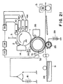
- Figure 2 shows an outline of an example of a full-color image forming apparatus using no intermediate transfer member.
- Laser light emitted from a laser (not shown) driven based on image signals is reflected by a rotating polygonal mirror 201 and a mirror 202 to be incident to a primarily charged photosensitive member 204.
- the photosensitive member 204 rotates in an indicated arrow direction during which the photosensitive member is exposed to scanning laser light in the above-described manner to form an electrostatic latent image sequentially thereon.
- the thus-formed electrostatic latent image is developed by a rotating developing device 203, and the developed toner image is then transferred onto a transfer(-receiving) paper 206 wound about a transfer drum 205.
- These steps are repeated in totally four cycles sequentially for Y (yellow), M (magenta), C (cyan) and BK (black), respectively, to form a full color image.
- the transfer paper 206 is separated from the transfer drum 205, and subjected to fixing by a pair of fixing rollers 207 to form a full-color image print.
- the above-mentioned pattern formed for controlling the image forming conditions is also obtained in the above-described manner.
- An LED 208 issuing near infrared rays (having a principal wavelength at ca. 950 nm) is used as an illumination means for illuminating the photosensitive member, and reflected light from the photosensitive member is read by a sensor 209.
- the image forming conditions may be controlled according to methods, e.g., as disclosed in U.S. Patents Nos. 4,312,589, 5,258,783 and 5,296,903, and JP-A 5-53402, thereby obtaining best full color images under the respective conditions.
- the intermediate transfer member is required to have a preferred level of resistivity (1x10 4 - 1x10 13 ohm.cm) and a high mechanical strength.
- the intermediate transfer member generally requires the inclusion of a large amount of filler, such as carbon black.
- the resultant intermediate transfer member becomes opaque and provides a lower reflectance to light, thus making difficult an accurate density measurement of a pattern formed thereon especially with respect to a black toner pattern.
- An object of the present invention is to provide an image forming apparatus allowing a better accuracy of pattern density measurement for controlling image forming conditions and capable of providing best images under available conditions.
- Another object of the present invention is to provide an image forming apparatus allowing a broader latitude for pattern density measurement designing.
- a further object of the present invention is to provide an intermediate transfer member suitable for use in an image forming apparatus as described above.
- an image forming apparatus comprising:
- an intermediate transfer member having the above-mentioned reflectance characteristic for use in an image forming apparatus as described above.
- a large reflectance difference between a black toner (reflectance on the order of below 10 %) and other color toners (reflectance on the order of 80 % or higher) is utilized, and the reflectance of the intermediate transfer member is adjusted to an intermediate level between the two levels to provide a good contrast with both a lack toner pattern and other color toner patterns, instead of providing different reflectance regions for different color toners.
- Figure 1 is an illustration of an image forming apparatus including an intermediate transfer member.
- Figure 2 is an illustration of an image forming apparatus including no intermediate transfer member.
- Figures 3 - 6 are graphs showing spectral reflectance characteristics of yellow toner, magenta toner, cyan toner and black toner, respectively.
- Figures 7 - 9 are graphs each showing a spectral reflectance characteristic of an intermediate transfer member suitable for use in the invention.
- Figure 10 is a graph showing a spectral radiation intensity characteristic of light used for image density measurement.
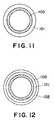
- Figures 11 and 12 are respectively a diametrical sectional view of a drum-shaped intermediate transfer member used in the invention.
- Figure 13 is an illustration of an image forming apparatus including an intermediate transfer member in the form of an endless belt.
- Figures 14 - 16 are perspective illustrations of drum-shaped intermediate transfer members usable in the invention having specified reflectance portions in the form of a longitudinal stripe, a circumferential stripe and a square, respectively.
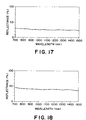
- Figures 17 - 20 are graphs showing spectral reflectance characteristic of intermediate transfer members prepared in Example 1, Example 2, Comparative Example 1 and Comparative Example 2, respectively.
- Figures 21 and 22 are respectively an illustration of an embodiment of the image forming apparatus according to the invention.
- the image forming apparatus basically includes a first image-bearing member, and an intermediate transfer member for receiving an image formed on the first image-bearing member and transferring the image onto a second image-bearing member.
- the image forming apparatus further includes pattern-forming means for forming a prescribed pattern on the intermediate transfer member, density detection means for detecting a density of the pattern, and control means for controlling image forming conditions based on the detected density.
- the intermediate transfer member is designed to have a reflectance of 10 - 70 % for light having a wavelength in the range of 700 - 1500 nm at least in a region thereof for forming the prescribed pattern.
- yellow, magenta and cyan toners have spectral reflectance characteristic as shown in Figures 3 - 5, respectively, and show reflectance of at least 80 % for light having a wavelength in the range of 700 - 1500 nm.
- a black toner e.g., a mono-component magnetic toner
- the intermediate transfer member is designed to have a reflectance of 10 - 70 %, preferably 15 - 60 %, further preferably 15 - 35 %, at least in a pattern density-detection region thereof for light having a wavelength in the range of 700 - 1500 nm, e.g., at a near infrared wavelength of ca. 950 nm, thereby allowing the density detection of all of black and color images at an improved accuracy.
- the intermediate transfer member need not show an overall reflectance of 10 - 70 % for light having wavelengths ranging from 700 to 1500 nm. It is sufficient if the intermediate transfer member shows a spectral reflectance of 10 -70 % for a light fraction having a specific wavelength in the range of 700 - 1500 nm even if the intermediate transfer member shows a spectral reflectance of below 10 % (or above 70 %) at another wavelength in the same range as shown in Figure 7 (showing a spectral reflectance of ca. 23 % at 950 nm). In such a case, a stable and accurate image density is still possible by using a detection means including a light source issuing infrared rays having a principal or peak wavelength at or near the specific wavelength.
- an intermediate transfer member showing a spectral reflectance exceeding 70 % at some wavelength can also be used if it also shows a spectral reflectance in the range of 10 - 70 % at a specific wavelength in the range of 700 - 1500 nm as shown in Figure 8 (showing a spectral reflectance of ca. 33 % at 1000 nm).
- a stable and accurate density detection is also possible by using a photodetection system using infrared rays having a principal wavelength at or near the specific wavelength (1000 nm).
- the light used for the density detection should have a principal wavelength in the range of 700 - 1500 nm as a matter of course but may preferably have a principal wavelength in the range of 800 - 1100 nm, particularly 900 - 1000 nm, in view of the stability of reflectance for the color toners.
- the reflectances of toners and intermediate transfer members referred to herein are based on values measured by using a commercially available apparatus ("U-3400", available from Hitachi Seisakusho K.K.) equipped with a large sample chamber integrating sphere at scanning speeds of 300 nm/min for visible region and 600 nm/min for infrared region, a response level of medium, and band passes of 5.00 nm for visible region and servo (variable) for infrared region.
- U-3400 available from Hitachi Seisakusho K.K.
- the intermediate transfer member used in the present invention may have a structure including at least an electroconductive support and an elastic layer thereon comprising rubber, elastomer or resin, optionally further one or more coating layers thereon.
- the intermediate transfer member may have various shapes including drums or rollers as shown in Figures 11 and 12 and an endless belt (103) as shown in Figure 13, which may be arbitrarily selected depending on the purpose or necessity.
- Figures 11 and 12 show drum-shaped intermediate transfer members including a cylindrical electroconductive support 100 and an elastic layer 101, and further a coating layer 102.
- the endless belt-shaped intermediate transfer member 103 ( Figure 13) may also have a similar lamination structure although the outer shape is different.
- the intermediate transfer member may preferably be in the form of a drum or roller in view of little color deviation in superposition of colors and durability in repetitive use.
- the electroconductive support (100) may preferably comprise a metal or alloy, such as aluminum, iron, copper or stainless steel, or an electroconductive resin containing electroconductive carbon or metal particles.
- the support may have a shape of a drum or an endless belt as described above, inclusive of a drum equipped with a shaft piercing therethrough and a cylindrical bar.
- the elastic layer (101) and the coating layer (102) of the intermediate transfer member used in the present invention may comprise a rubber or elastomer, or a resin.
- the rubber or elastomer may include: styrene-butadiene rubber, high-styrene rubber, butadiene rubber, isoprene rubber, ethylenepropylene copolymer, nitrile-butadiene rubber, chloroprene rubber, butyl rubber, silicone rubber, fluorine-containing rubber, nitrile rubber, urethane rubber, acrylic rubber, epichlorohydrin rubber, and norbornene rubber.
- the resin may include: styrene-based resins (homopolymers and copolymers of styrene and substituted styrene, inclusive of polystyrene, chloropolystyrene, poly- ⁇ -methylstyrene, styrene-butadiene copolymer, styrene-vinyl chloride copolymer, styrene-vinyl acetate copolymer, styrenemaleic acid copolymer), styrene-acrylate copolymers (such as styrene-methyl acrylate copolymer, styrene-ethyl acrylate copolymer, styrene-butyl acrylate copolymer, styrene-octyl acrylate copolymer, and styrene-phenyl acrylate copolymer), styrene-based
- the intermediate transfer member may preferably have a resistivity on the order of 1x10 4 - 1x10 13 ohm.cm.
- the elastic layer or the coating layer may contain an electroconductive substance dispersed therein or comprise an electroconductive resin.
- electroconductive substance may include: electroconductive carbon black; and electroconductive materials inclusive of metals such as aluminum and nickel; electroconductive metal oxides, such as electroconductive titanium oxide, electroconductive tin oxide, electroconductive zinc oxide and electroconductive zinc oxide and electroconductive indium oxide; and electroconductive polymeric compounds, such as quaternary ammonium salt-containing polymethyl methacrylate, polyvinylaniline, polyvinylpyrrole, polydiacetylene, polyethyleneimine, boron-containing polymers and polypyrrole. These may be used singly or in combination of two or more species. These are however not exhaustive.
- the resultant intermediate transfer member is liable to have an excessively high transmittance so that it becomes also difficult to provide a sufficient density contrast with yellow toner, magenta toner and cyan toner having a high resistance. In this case, it is also effective to positively lower the reflectance of the intermediate transfer member according to the present invention.
- the intermediate transfer member may preferably contain a lubricating in its surface layer so as to exhibit an improved releasability.
- Examples of the lubricating substance may include: tetrafluoroethylene resin, trifluorochloroethylene resin, tetrafluoroethylene-hexafluoropropylene copolymer resin, vinyl fluoride resin, vinylidene fluoride resin, difluorodichloro-ethylene resin, fluorinated carbon, silicone resin, silicone rubber, silicone elastomer, polyethylene (PE), polypropylene (PP), polystyrene (PS), acrylic resin, nylon resin, phenolic resin, epoxy resin, silica, and alumina. These may be used singly or in combination of two or more species. Among these, tetrafluoroethylene resin and tetrafluoroethylene-hexafluoropropylene copolymer resin are particularly preferred.
- the elastic layer (101) may preferably have a thickness of at least 0.5 mm, more preferably at least 1 mm, further preferably 1 - 10 mm.
- the coating layer (102) may preferably be thin so as to conduct the softness of the lower elastic layer to the surface of the intermediate transfer member and more specifically have a thickness of at most 3 mm, more preferably at most 2 mm, further preferably 20 ⁇ m - 1 mm.
- the intermediate transfer member may be set to have a reflectance in the above-mentioned specific range by incorporating a reflectance-adjusting pigment into the coating layer and/or the elastic layer, and/or controlling the thickness of the coating layer.
- Examples of the reflectance-adjusting pigment incorporated in the coating layer and/or the elastic layer may include; white pigments, such as titanium oxide (such as titanium white), barium sulfate, and zinc white; value pigments, such as phthalocyanine blue; red pigments, such as dimethylquinacridone, yellow pigments, such as disazo yellow, and black pigments, such as a relatively small amount of carbon black.
- white pigments are preferred because of coloring ability
- titanium white is particularly preferred because of coloring ability and dispersibility.
- the pigment may preferably be contained in a proportion of 0.2 - 10 wt. parts, particularly 1 - 3 wt. parts, per 100 wt. parts of the elastomer and the resin in the layer in which the pigment is contained.
- the pigment may preferably be contained in a proportion of 0.05 - 0.5 wt. part per 100 wt. parts of the elastomer and the resin in the layer concerned.
- the coating layer thickness may preferably be adjusted in the range of at most 3 ⁇ m, more preferably at most 2 mm, further preferably 0.02 ⁇ m - 1 mm.
- a pigment in a layer which may preferably be not the uppermost surface layer but an intermediate layer so as to retain the required properties, such as strength, releasability, water-repellency and electroconductivity, of the surface layer of the intermediate transfer member functioning to directly receive an image transferred thereto and transferring the received imaged to a second image-bearing member, unlike the transfer drum.
- the present invention controlling the reflectance of the intermediate transfer member is also effective in providing a broader latitude of designing to the photosensitive member, in addition to the provision of more accurate density data.
- the present invention does not require a special light source or a sensor with an extremely high accuracy compared with a system using an intermediate transfer member having a reflectance not satisfying the requirement of the present invention. Also, in this respect, a broad latitude of designing is provided.
- the intermediate transfer member need not have the specific resistance over the entire surface thereof but it is sufficient that the intermediate transfers member has a surface region at least locally showing the specific reflectance where the pattern density is measured.
- the intermediate transfer member may have a longitudinal stripe region (as shown in Figure 14), a circumferential stripe region (as shown in Figure 15) or a local pattern of, e.g., a square (as shown in Figure 16) showing the specific reflectance.
- the intermediate transfer member may preferably have the specific reflectance over the entire surface.
- the density measurement pattern-forming method, the shape of the pattern, the pattern density-measurement means, the control means for controlling image forming conditions based on the detected pattern density, the timing of the control, etc. need not be particularly limited, but may be selected according to the known techniques.
- the pattern may include a succession of square images having several density levels, which may be provided for the respective colors.
- the optical system for density detection may for example include a light source of, e.g., an LED emitting light having a principal wavelength around 950 nm, and a sensor of, e.g., silicon photo-diode. Based on the detected pattern density, it may be possible to control, e.g., the developing bias, the spot diameter of exposure light for exposing the first image-bearing member, and the quantity of replenished toner.
- the first image-bearing member used in the present invention may suitably comprise an electrophotographic photosensitive member, of which the structure and composition need not be particularly limited.
- the second image-bearing member used in the present invention may include various types of paper and OHP sheets.
- EPDM ethylene-propylene-diene copolymer rubber
- 5 wt. parts of zinc oxide 1 wt. part of higher fatty acid
- 5 wt. parts of electroconductive carbon 10 wt. parts of paraffin oil
- MTT 2-mercaptobenzothiazole
- TMTD tetramethylthiuram disulfide
- ZnMDD zinc dimethyldithiocarbamate
- the elastic layer compound was transfer-molded and vulcanized to form a 5 mm-thick elastic layer, which was then coated with the surface layer paint by spray coating to form a 40 ⁇ m-thick surface layer, thereby obtaining an intermediate transfer member.
- the reflectance of the thus-obtained intermediate transfer member was measured according to the above-described manner to obtain a spectral reflectance characteristic as shown in Figure 17.
- the intermediate transfer member was incorporated in an electrophotographic photosensitive member (shown in Figure 21) having a structure generally as shown in Figure 1, and also including a density detection circuit 53 for detecting a density of pattern formed on the intermediate transfer member and a control circuit 54 for controlling the image forming conditions, particularly for controlling a developing bias generating circuit 55 in this example, whereby the pattern formation and the pattern density measurement were performed.
- the density measurement pattern included a succession of 5 squares at 5 density levels from a maximum density to a minimum density for each of yellow, magenta, cyan and black.
- the light source 51 for the pattern density measurement was an LED (light emission device) emitting light having a principal wavelength of 950 nm.
- the density levels of the thus-formed pattern were measured by using a silicon photodiode 52, whereby totally 20 density levels (5 levels for each of the four colors of yellow, magenta, cyan and black) were accurately measured and the measured density levels were satisfactorily used for controlling the developing bias voltages.
- EPDM 100 wt. parts of EPDM, 5 wt. parts of zinc oxide, 5 wt. parts of titanium white (colorant), 150 wt. parts of electroconductive titanium oxide, 10 wt. parts of paraffin oil, 2 wt. parts of sulfur, and totally 4 weight parts of vulcanization promoters (1 wt. part of MBT, 1.5 wt. parts of TMTD and 1.5 wt. parts of ZnMDC) were blended by a two-roll mill under cooling for 20 min to prepare a compound.
- An intermediate transfer member was prepared in the same manner as in Example 1 except for using the above-prepared elastic layer compound and surface layer paint. As a result, the intermediate transfer member showed a spectral reflectance characteristic as shown in Figure 18.
- the intermediate transfer member was incorporated in the same electrophotographic image forming apparatus as in Example 1 and evaluated in the same manner as in Example 1, whereby all the density levels for the respective colors were accurately measured, and the control of the developing biases was satisfactorily performed.
- a surface layer paint was prepared in the same manner as in Example 1 except that the amount of PTFE particles were reduced to 50 wt. parts.
- the elastic layer compound was vulcanized in a mold at 150 °C for 50 min. to form an endless belt having an outer diameter of 150 mm, a width of 230 mm and a thickness of 0.9 mm.
- the above-prepared surface layer paint was applied by spray coating to form a 30 ⁇ m-thick surface layer, thereby obtaining an intermediate transfer member.
- the intermediate transfer member showed a reflectance in the range of 10 - 70 % (somewhat lower level than in Figure 17) in the range of 700 - 1500 nm.
- the intermediate transfer member was incorporated in an electrophotographic image forming apparatus shown in Figure 22 (generally similar to one shown in Figure 13 but further including an LED 51, a silicon photodiode 52, a density detection circuit 53, a control circuit 54 and a developing bias supply 55 similar to those used in Example 1), whereby all the density levels for the respective colors were accurately measured, and the control of the developing bias voltages was satisfactorily performed.
- An intermediate transfer member was prepared in the same manner as in Example 1 except that surface layer paint was replaced by the one of Example 2 to form a 25 ⁇ m-thick surface layer.
- the resultant intermediate transfer member showed a spectral reflectance characteristic as shown in Figure 19 showing a reflectance of below 10 % over the range of 700 nm to 1500 nm.
- the intermediate transfer member was incorporated in the same electrophotographic image forming apparatus as in Example 1 and evaluated in the same manner as in Example 1, whereby all the density levels could be measured for yellow, magenta and cyan but the pattern density detection was impossible for black because of too low a spectral reflectance difference.
- An intermediate transfer member was prepared in the same manner as in Example 1 except that the elastic layer compound and the surface layer paint were replaced by those described above.
- the resultant intermediate transfer member showed a spectral reflectance characteristic as shown in Figure 20 showing a reflectance of ca. 80 - 90 % over the range of 700 nm to 1500 nm.
- the intermediate transfer member was incorporated in the same electrophotographic image forming apparatus as in Example 1 and evaluated in the same manner as in Example 1, whereby all the density levels could be measured for black but the pattern density detection was impossible for yellow, magenta or cyan because of the excessively high reflectance of the intermediate transfer member.
Landscapes
- Physics & Mathematics (AREA)
- General Physics & Mathematics (AREA)
- Engineering & Computer Science (AREA)
- Microelectronics & Electronic Packaging (AREA)
- Electrostatic Charge, Transfer And Separation In Electrography (AREA)
- Color Electrophotography (AREA)
Applications Claiming Priority (3)
| Application Number | Priority Date | Filing Date | Title |
|---|---|---|---|
| JP10237895 | 1995-04-26 | ||
| JP102378/95 | 1995-04-26 | ||
| JP10237895 | 1995-04-26 |
Publications (2)
| Publication Number | Publication Date |
|---|---|
| EP0740221A1 true EP0740221A1 (fr) | 1996-10-30 |
| EP0740221B1 EP0740221B1 (fr) | 2001-10-10 |
Family
ID=14325804
Family Applications (1)
| Application Number | Title | Priority Date | Filing Date |
|---|---|---|---|
| EP96302912A Expired - Lifetime EP0740221B1 (fr) | 1995-04-26 | 1996-04-25 | Appareil de formation d'images et élément de transfert intermédiaire |
Country Status (3)
| Country | Link |
|---|---|
| US (1) | US5842080A (fr) |
| EP (1) | EP0740221B1 (fr) |
| DE (1) | DE69615734T2 (fr) |
Cited By (4)
| Publication number | Priority date | Publication date | Assignee | Title |
|---|---|---|---|---|
| EP0740222A3 (fr) * | 1995-04-28 | 1997-05-28 | Canon Kk | Composition de revêtement électroconductrice blanche et élément porteur de matériau de transfert |
| EP0840175A3 (fr) * | 1996-11-01 | 1999-11-10 | Canon Kabushiki Kaisha | Un appareil de formation d'images |
| WO2000041038A1 (fr) * | 1999-01-05 | 2000-07-13 | Oce Printing Systems Gmbh | Procede et dispositif pour reguler la concentration de toner dans un procede electrographique |
| WO2001058135A3 (fr) * | 2000-02-04 | 2001-12-20 | Oce Printing Systems Gmbh | Procede et dispositif de regulation de la concentration de toner dans un processus electrographique |
Families Citing this family (20)
| Publication number | Priority date | Publication date | Assignee | Title |
|---|---|---|---|---|
| US5995794A (en) * | 1997-02-28 | 1999-11-30 | Canon Kabushiki Kaisha | Image forming apparatus and intermediate transfer belt |
| JP3228190B2 (ja) * | 1997-07-01 | 2001-11-12 | 富士ゼロックス株式会社 | 両面画像形成装置 |
| US6044234A (en) * | 1997-09-11 | 2000-03-28 | Canon Kabushiki Kaisha | Image processing apparatus and method for controlling a detection timing of a density sensor |
| US5966573A (en) * | 1998-10-08 | 1999-10-12 | Xerox Corporation | Seamed flexible electrostatographic imaging belt having a permanent localized solid attribute |
| JP2000275980A (ja) * | 1999-03-23 | 2000-10-06 | Canon Inc | 中間転写体、中間転写体の製造方法及び画像形成装置 |
| JP4011826B2 (ja) * | 1999-05-10 | 2007-11-21 | キヤノン株式会社 | 画像形成装置 |
| JP2001022194A (ja) | 1999-07-07 | 2001-01-26 | Canon Inc | ベルト状転写部材、該ベルト状転写部材の製造方法及び画像形成装置 |
| JP4365954B2 (ja) | 1999-10-22 | 2009-11-18 | キヤノン株式会社 | ベルト及びこれを備える画像形成装置 |
| JP3619140B2 (ja) * | 1999-10-28 | 2005-02-09 | キヤノン株式会社 | 画像形成装置 |
| CN1252547C (zh) | 2000-02-03 | 2006-04-19 | 佳能株式会社 | 制作用于转印系统的转印件的方法 |
| JP2002072609A (ja) * | 2000-08-31 | 2002-03-12 | Canon Inc | 画像形成装置 |
| US6611666B2 (en) | 2001-06-15 | 2003-08-26 | Nexpress Solutions Llc | Densitometer with improved accuracy for use in color image processing apparatus |
| EP1329774B1 (fr) * | 2002-01-18 | 2006-12-20 | Canon Kabushiki Kaisha | Révélateur coloré et méthode de production d'images multicolores |
| JP2004094177A (ja) * | 2002-04-26 | 2004-03-25 | Canon Inc | 電子写真エンドレスベルト、プロセスカートリッジおよび電子写真装置 |
| JP4289981B2 (ja) * | 2003-07-14 | 2009-07-01 | キヤノン株式会社 | トナー及び画像形成方法 |
| US20050214015A1 (en) * | 2004-03-25 | 2005-09-29 | Eastman Kodak Company | Densitometer for use in a printer |
| DE102006007509B4 (de) * | 2006-02-16 | 2009-01-22 | Contitech Antriebssysteme Gmbh | Keilrippenriemen mit verbessertem Geräuschverhalten |
| US8187711B2 (en) * | 2009-10-29 | 2012-05-29 | Xerox Corporation | Polymeric intermediate transfer members |
| JP5790046B2 (ja) * | 2011-03-16 | 2015-10-07 | 株式会社リコー | 画像形成装置及び画像濃度制御方法 |
| JP6238692B2 (ja) * | 2012-12-07 | 2017-11-29 | キヤノン株式会社 | 導電性ベルトおよび電子写真装置 |
Citations (6)
| Publication number | Priority date | Publication date | Assignee | Title |
|---|---|---|---|---|
| JPS5913264A (ja) * | 1982-07-14 | 1984-01-24 | Canon Inc | 画像形成装置 |
| US5103260A (en) * | 1990-10-29 | 1992-04-07 | Colorocs Corporation | Toner density control for electrophotographic print engine |
| US5258783A (en) * | 1991-02-22 | 1993-11-02 | Canon Kabushiki Kaisha | Image processing method and apparatus with gamma-correction control |
| JPH05333725A (ja) * | 1992-05-29 | 1993-12-17 | Canon Inc | 画像形成装置 |
| EP0604941A2 (fr) * | 1992-12-28 | 1994-07-06 | Canon Kabushiki Kaisha | Appareil de formation d'images |
| US5438398A (en) * | 1992-05-29 | 1995-08-01 | Canon Kabushiki Kaisha | Image forming apparatus with intermediate transfer member |
Family Cites Families (8)
| Publication number | Priority date | Publication date | Assignee | Title |
|---|---|---|---|---|
| US4312589A (en) * | 1979-11-19 | 1982-01-26 | International Business Machines Corporation | Charge density control for an electrostatic copier |
| EP0275636B1 (fr) * | 1987-01-19 | 1993-07-21 | Canon Kabushiki Kaisha | Agent de contraste coloré et développateur à deux composants, le contenant |
| JP2836908B2 (ja) * | 1990-05-11 | 1998-12-14 | 三菱重工業株式会社 | 型厚調整装置 |
| EP0501497B1 (fr) * | 1991-03-01 | 1996-01-03 | Canon Kabushiki Kaisha | Système de formation d'images et unité amovible, de traitement montée sur celui-ci |
| JPH0553402A (ja) * | 1991-08-26 | 1993-03-05 | Canon Inc | 画像形成装置 |
| JP3035397B2 (ja) * | 1991-10-18 | 2000-04-24 | キヤノン株式会社 | 画像形成装置 |
| JPH06175452A (ja) * | 1992-12-11 | 1994-06-24 | Matsushita Electric Ind Co Ltd | 電子写真装置 |
| US5625857A (en) * | 1994-01-18 | 1997-04-29 | Hitachi, Ltd. | Image forming apparatus which measures deposit amounts of toner |
-
1996
- 1996-04-25 DE DE69615734T patent/DE69615734T2/de not_active Expired - Lifetime
- 1996-04-25 EP EP96302912A patent/EP0740221B1/fr not_active Expired - Lifetime
-
1997
- 1997-03-07 US US08/813,678 patent/US5842080A/en not_active Expired - Lifetime
Patent Citations (6)
| Publication number | Priority date | Publication date | Assignee | Title |
|---|---|---|---|---|
| JPS5913264A (ja) * | 1982-07-14 | 1984-01-24 | Canon Inc | 画像形成装置 |
| US5103260A (en) * | 1990-10-29 | 1992-04-07 | Colorocs Corporation | Toner density control for electrophotographic print engine |
| US5258783A (en) * | 1991-02-22 | 1993-11-02 | Canon Kabushiki Kaisha | Image processing method and apparatus with gamma-correction control |
| JPH05333725A (ja) * | 1992-05-29 | 1993-12-17 | Canon Inc | 画像形成装置 |
| US5438398A (en) * | 1992-05-29 | 1995-08-01 | Canon Kabushiki Kaisha | Image forming apparatus with intermediate transfer member |
| EP0604941A2 (fr) * | 1992-12-28 | 1994-07-06 | Canon Kabushiki Kaisha | Appareil de formation d'images |
Non-Patent Citations (1)
| Title |
|---|
| PATENT ABSTRACTS OF JAPAN vol. 008, no. 101 (P - 273) 12 May 1984 (1984-05-12) * |
Cited By (6)
| Publication number | Priority date | Publication date | Assignee | Title |
|---|---|---|---|---|
| EP0740222A3 (fr) * | 1995-04-28 | 1997-05-28 | Canon Kk | Composition de revêtement électroconductrice blanche et élément porteur de matériau de transfert |
| US5824408A (en) * | 1995-04-28 | 1998-10-20 | Canon Kabushiki Kaisha | White electroconductive coating composition and transfer material-carrying member |
| EP0840175A3 (fr) * | 1996-11-01 | 1999-11-10 | Canon Kabushiki Kaisha | Un appareil de formation d'images |
| WO2000041038A1 (fr) * | 1999-01-05 | 2000-07-13 | Oce Printing Systems Gmbh | Procede et dispositif pour reguler la concentration de toner dans un procede electrographique |
| US6498909B1 (en) | 1999-01-05 | 2002-12-24 | Oce Printing Systems Gmbh | Method and apparatus for controlling the toner concentration in an electrographic process |
| WO2001058135A3 (fr) * | 2000-02-04 | 2001-12-20 | Oce Printing Systems Gmbh | Procede et dispositif de regulation de la concentration de toner dans un processus electrographique |
Also Published As
| Publication number | Publication date |
|---|---|
| DE69615734D1 (de) | 2001-11-15 |
| US5842080A (en) | 1998-11-24 |
| EP0740221B1 (fr) | 2001-10-10 |
| DE69615734T2 (de) | 2002-08-01 |
Similar Documents
| Publication | Publication Date | Title |
|---|---|---|
| EP0740221B1 (fr) | Appareil de formation d'images et élément de transfert intermédiaire | |
| EP0752628B1 (fr) | Appareil et méthode de formation d'images | |
| US5915144A (en) | Multicolor image forming method | |
| KR0171167B1 (ko) | 화상 형성 장치 | |
| US6920299B2 (en) | Image forming apparatus and intermediate transfer unit detachably mountable thereon | |
| EP0747785B1 (fr) | Appareil de formation d'images et élément de transfert intermédiaire | |
| EP1280018A1 (fr) | Appareil de formation d'images utilisant un élément de transfert intermédiaire | |
| EP0860751B1 (fr) | Appareil de formation d'images | |
| US20040191665A1 (en) | Method for forming an image | |
| JP3372752B2 (ja) | 画像形成装置、中間転写体及び中間転写体の製造方法 | |
| JP3612867B2 (ja) | カラー画像形成装置 | |
| US6587659B2 (en) | Image forming device | |
| JP3368130B2 (ja) | 画像形成装置及び中間転写体の製造方法 | |
| JP2005234081A (ja) | 画像形成装置及び画像形成方法 | |
| US20070003848A1 (en) | Image forming method, a processing cartridge and an image forming method using the same | |
| JP3674251B2 (ja) | 画像記録装置 | |
| JP4971737B2 (ja) | 画像形成装置 | |
| JPH11327316A (ja) | 画像形成装置 | |
| US6560420B2 (en) | Electrophotographic device for transferring a plural color toner image | |
| JP2004233973A (ja) | 画像形成方法及びトナー | |
| JP2002023433A (ja) | 画像形成装置 | |
| JP3747603B2 (ja) | 画像形成方法 | |
| JP2004177461A (ja) | 画像形成方法及び画像形成装置 | |
| US20180011428A1 (en) | Transfer belt and image forming apparatus | |
| JPH07219302A (ja) | 画像形成装置 |
Legal Events
| Date | Code | Title | Description |
|---|---|---|---|
| PUAI | Public reference made under article 153(3) epc to a published international application that has entered the european phase |
Free format text: ORIGINAL CODE: 0009012 |
|
| AK | Designated contracting states |
Kind code of ref document: A1 Designated state(s): DE FR GB IT |
|
| 17P | Request for examination filed |
Effective date: 19970312 |
|
| 17Q | First examination report despatched |
Effective date: 19990616 |
|
| GRAG | Despatch of communication of intention to grant |
Free format text: ORIGINAL CODE: EPIDOS AGRA |
|
| GRAG | Despatch of communication of intention to grant |
Free format text: ORIGINAL CODE: EPIDOS AGRA |
|
| GRAG | Despatch of communication of intention to grant |
Free format text: ORIGINAL CODE: EPIDOS AGRA |
|
| GRAH | Despatch of communication of intention to grant a patent |
Free format text: ORIGINAL CODE: EPIDOS IGRA |
|
| GRAG | Despatch of communication of intention to grant |
Free format text: ORIGINAL CODE: EPIDOS AGRA |
|
| GRAH | Despatch of communication of intention to grant a patent |
Free format text: ORIGINAL CODE: EPIDOS IGRA |
|
| GRAH | Despatch of communication of intention to grant a patent |
Free format text: ORIGINAL CODE: EPIDOS IGRA |
|
| GRAA | (expected) grant |
Free format text: ORIGINAL CODE: 0009210 |
|
| AK | Designated contracting states |
Kind code of ref document: B1 Designated state(s): DE FR GB IT |
|
| REF | Corresponds to: |
Ref document number: 69615734 Country of ref document: DE Date of ref document: 20011115 |
|
| ET | Fr: translation filed | ||
| REG | Reference to a national code |
Ref country code: GB Ref legal event code: IF02 |
|
| PLBE | No opposition filed within time limit |
Free format text: ORIGINAL CODE: 0009261 |
|
| STAA | Information on the status of an ep patent application or granted ep patent |
Free format text: STATUS: NO OPPOSITION FILED WITHIN TIME LIMIT |
|
| 26N | No opposition filed | ||
| PGFP | Annual fee paid to national office [announced via postgrant information from national office to epo] |
Ref country code: GB Payment date: 20140414 Year of fee payment: 19 |
|
| PGFP | Annual fee paid to national office [announced via postgrant information from national office to epo] |
Ref country code: FR Payment date: 20140428 Year of fee payment: 19 Ref country code: DE Payment date: 20140430 Year of fee payment: 19 Ref country code: IT Payment date: 20140402 Year of fee payment: 19 |
|
| REG | Reference to a national code |
Ref country code: DE Ref legal event code: R119 Ref document number: 69615734 Country of ref document: DE |
|
| GBPC | Gb: european patent ceased through non-payment of renewal fee |
Effective date: 20150425 |
|
| PG25 | Lapsed in a contracting state [announced via postgrant information from national office to epo] |
Ref country code: IT Free format text: LAPSE BECAUSE OF NON-PAYMENT OF DUE FEES Effective date: 20150425 Ref country code: GB Free format text: LAPSE BECAUSE OF NON-PAYMENT OF DUE FEES Effective date: 20150425 Ref country code: DE Free format text: LAPSE BECAUSE OF NON-PAYMENT OF DUE FEES Effective date: 20151103 |
|
| REG | Reference to a national code |
Ref country code: FR Ref legal event code: ST Effective date: 20151231 |
|
| PG25 | Lapsed in a contracting state [announced via postgrant information from national office to epo] |
Ref country code: FR Free format text: LAPSE BECAUSE OF NON-PAYMENT OF DUE FEES Effective date: 20150430 |