EP0740423B1 - Digitaler Phasenregelkreis - Google Patents
Digitaler Phasenregelkreis Download PDFInfo
- Publication number
- EP0740423B1 EP0740423B1 EP96302922A EP96302922A EP0740423B1 EP 0740423 B1 EP0740423 B1 EP 0740423B1 EP 96302922 A EP96302922 A EP 96302922A EP 96302922 A EP96302922 A EP 96302922A EP 0740423 B1 EP0740423 B1 EP 0740423B1
- Authority
- EP
- European Patent Office
- Prior art keywords
- phase
- stage frequency
- clock
- outputs
- pulse
- Prior art date
- Legal status (The legal status is an assumption and is not a legal conclusion. Google has not performed a legal analysis and makes no representation as to the accuracy of the status listed.)
- Expired - Lifetime
Links
- 230000003111 delayed effect Effects 0.000 claims description 25
- 230000001360 synchronised effect Effects 0.000 claims description 10
- 230000001105 regulatory effect Effects 0.000 claims description 8
- 230000002860 competitive effect Effects 0.000 claims description 7
- 238000010586 diagram Methods 0.000 description 7
- 238000005070 sampling Methods 0.000 description 6
- 230000008030 elimination Effects 0.000 description 4
- 238000003379 elimination reaction Methods 0.000 description 4
- 230000000630 rising effect Effects 0.000 description 2
- 238000010276 construction Methods 0.000 description 1
- 230000001276 controlling effect Effects 0.000 description 1
- 238000000354 decomposition reaction Methods 0.000 description 1
- 230000003247 decreasing effect Effects 0.000 description 1
- 238000001514 detection method Methods 0.000 description 1
- 230000000694 effects Effects 0.000 description 1
Images


Classifications
-
- H—ELECTRICITY
- H04—ELECTRIC COMMUNICATION TECHNIQUE
- H04J—MULTIPLEX COMMUNICATION
- H04J3/00—Time-division multiplex systems
- H04J3/02—Details
- H04J3/06—Synchronising arrangements
- H04J3/062—Synchronisation of signals having the same nominal but fluctuating bit rates, e.g. using buffers
- H04J3/0632—Synchronisation of packets and cells, e.g. transmission of voice via a packet network, circuit emulation service [CES]
-
- H—ELECTRICITY
- H03—ELECTRONIC CIRCUITRY
- H03L—AUTOMATIC CONTROL, STARTING, SYNCHRONISATION OR STABILISATION OF GENERATORS OF ELECTRONIC OSCILLATIONS OR PULSES
- H03L7/00—Automatic control of frequency or phase; Synchronisation
- H03L7/06—Automatic control of frequency or phase; Synchronisation using a reference signal applied to a frequency- or phase-locked loop
- H03L7/08—Details of the phase-locked loop
- H03L7/085—Details of the phase-locked loop concerning mainly the frequency- or phase-detection arrangement including the filtering or amplification of its output signal
- H03L7/087—Details of the phase-locked loop concerning mainly the frequency- or phase-detection arrangement including the filtering or amplification of its output signal using at least two phase detectors or a frequency and phase detector in the loop
-
- H—ELECTRICITY
- H03—ELECTRONIC CIRCUITRY
- H03L—AUTOMATIC CONTROL, STARTING, SYNCHRONISATION OR STABILISATION OF GENERATORS OF ELECTRONIC OSCILLATIONS OR PULSES
- H03L7/00—Automatic control of frequency or phase; Synchronisation
- H03L7/06—Automatic control of frequency or phase; Synchronisation using a reference signal applied to a frequency- or phase-locked loop
- H03L7/08—Details of the phase-locked loop
- H03L7/099—Details of the phase-locked loop concerning mainly the controlled oscillator of the loop
- H03L7/0991—Details of the phase-locked loop concerning mainly the controlled oscillator of the loop the oscillator being a digital oscillator, e.g. composed of a fixed oscillator followed by a variable frequency divider
- H03L7/0992—Details of the phase-locked loop concerning mainly the controlled oscillator of the loop the oscillator being a digital oscillator, e.g. composed of a fixed oscillator followed by a variable frequency divider comprising a counter or a frequency divider
- H03L7/0993—Details of the phase-locked loop concerning mainly the controlled oscillator of the loop the oscillator being a digital oscillator, e.g. composed of a fixed oscillator followed by a variable frequency divider comprising a counter or a frequency divider and a circuit for adding and deleting pulses
-
- H—ELECTRICITY
- H03—ELECTRONIC CIRCUITRY
- H03L—AUTOMATIC CONTROL, STARTING, SYNCHRONISATION OR STABILISATION OF GENERATORS OF ELECTRONIC OSCILLATIONS OR PULSES
- H03L7/00—Automatic control of frequency or phase; Synchronisation
- H03L7/06—Automatic control of frequency or phase; Synchronisation using a reference signal applied to a frequency- or phase-locked loop
- H03L7/16—Indirect frequency synthesis, i.e. generating a desired one of a number of predetermined frequencies using a frequency- or phase-locked loop
- H03L7/18—Indirect frequency synthesis, i.e. generating a desired one of a number of predetermined frequencies using a frequency- or phase-locked loop using a frequency divider or counter in the loop
- H03L7/183—Indirect frequency synthesis, i.e. generating a desired one of a number of predetermined frequencies using a frequency- or phase-locked loop using a frequency divider or counter in the loop a time difference being used for locking the loop, the counter counting between fixed numbers or the frequency divider dividing by a fixed number
- H03L7/191—Indirect frequency synthesis, i.e. generating a desired one of a number of predetermined frequencies using a frequency- or phase-locked loop using a frequency divider or counter in the loop a time difference being used for locking the loop, the counter counting between fixed numbers or the frequency divider dividing by a fixed number using at least two different signals from the frequency divider or the counter for determining the time difference
Definitions
- the present invention relates to a digital phase-locked loop (PLL) used in a cell decomposition circuit in an ATM or stuffing synchronization device.
- PLL digital phase-locked loop
- Fig. 1 of the accompanying drawings is a block schematic diagram illustrating a previously proposed digital PLL.
- an input clock F in and an output clock f out are inputted to first and second N-stage frequency dividers 11 and 12, respectively, and subjected to N-stage frequency division.
- Multilevel quantized phase comparator 13 which is driven by phase comparator clock Pf 0 , inputs the output clocks of N-stage frequency dividers 11 and 12 and outputs output phase error information (advanced pulses or delayed pulses) indicating the phase advance/phase delay of both output clocks.
- N1 counter 14 is a competitive counter which inputs the advanced pulses or delayed pulses, counts up in response to advanced pulses, and upon counting up to count value 2N 1 , both outputs an increment pulse and undergoes setting to initial value N 1 .
- N1 counter 14 counts down in response to delayed pulses, and upon counting down to "0,” both outputs a decrement pulse and undergoes setting to initial value N 1 .
- Frequency regulator 15 is driven by the standard drive clock Rf 0 of the digital PLL, and clears one pulse from the pulse train of standard drive clock Rf 0 when one increment pulse is generated from N1 counter 14 and adds one pulse to the pulse train of standard drive clock Rf 0 when one decrement pulse is generated from N1 counter 14.
- R-stage frequency divider 16 effects R-stage frequency division upon the output of frequency regulator 15 and outputs the output clock f out of the digital PLL.
- phase comparison is effected 1/N times that of a case in which N-stage frequency dividers are not employed.
- the gain of the switching network is reduced to 1/N, phase error information obtained per second drops to an insufficient level, and unwanted jitter (variations in phase) is generated.
- a digital PLL to be described below as an example are that half-clock phase control carried out in a frequency regulator can be detected in a phase comparator, the gain of a switching network can be maintained and the occurrence of unwanted jitter can be minimised.
- a digital PLL includes first N-stage frequency dividing means that N-stage frequency divides input clocks of a digital PLL and generates N clocks of a first phase, a second phase, ..., and an Nth phase synchronized to a first input clock, a second input clock, ..., and an Nth input clock, respectively, divides these N clocks into M groups (N>M), and outputs the result; second N-stage frequency dividing means that N-stage frequency divides output clocks of a digital PLL, generates N clocks of a first phase, a second phase, ..., and an Nth phase synchronized to a first output clock, a second output clock, ..., and an Nth output clock, respectively, divides these N clocks into M groups (N>M), and outputs the result; first multilevel quantized phase comparison means that inputs an arbitrary output signal of the first group of first N-stage frequency dividing means and an arbitrary output signal of the first group of second
- An N-order digital PLL within the scope of the appended claims includes the above-described digital PLL.
- first N-stage frequency dividing means that N-stage frequency divides input clocks of a digital PLL, generates N clocks of a first phase, a second phase, ..., and an Nth phase synchronized to a first input clock, a second input clock, ..., and an Nth input clock, respectively, divides these N clocks into M groups (N>M), and outputs the result;
- second N-stage frequency dividing means that N-stage frequency divides output clocks of a digital PLL, generates N clocks of a first phase, a second phase, ... and an Nth phase synchronized to a first output clock, a second output clock, ...
- first multilevel quantized phase comparison means that inputs an arbitrary output signal of the first group of first N-stage frequency dividing means and an arbitrary output signal of the first group of the second N-stage frequency dividing means and outputs the phase difference between the two signals in the form of advanced pulses indicating phase advance or delayed pulses indicating phase delay as a value quantized in multiple levels
- second multilevel quantized phase comparison means that inputs an arbitrary output signal of the second group of first N-stage frequency dividing means and an arbitrary output signal of the second group of second N-stage frequency dividing means and outputs the phase difference between the two signals as a value quantized in multiple levels
- Mth multilevel quantized phase comparison means that inputs an arbitrary output signal of the Mth group of first N-stage frequency dividing means and an arbitrary output signal of the Mth group of second N-stage frequency dividing means and outputs the phase difference between the two signals as a value quantized
- one pulse of advanced phase is generated from the adding means, and adds one pulse to the pulse train of the standard drive clock when one pulse of delayed phase is generated from the adding means; and R-stage frequency dividing means that R-stage frequency divides the output of the frequency regulating means and outputs an output clock of the digital PLL; wherein, of the M multilevel quantized phase comparison means, multilevel quantized phase comparison means of odd ordinal numbers are driven by a phase count clock of positive phase and multilevel quantized phase comparison means of even ordinal numbers are driven by a phase count clock of negative phase.
- An N-order digital PLL within the scope of the appended claims includes the above described another digital PLL.
- phase error information obtained in one second can be increased M-fold and the system gain can be increased M-fold. Moreover, generated phase jitter can be reduced because accurate phase error information can be obtained.
- a digital PLL which includes a first N-stage frequency divider 1, a second N-stage frequency divider 2, M multilevel quantized phase comparators 3-1 to 3-M, an adder 4, an N1 counter 5, a frequency regulator 6, and an R-stage frequency divider 7.
- First N-stage frequency divider 1 N-stage frequency divides input clock f in of the digital PLL, generates first phase, second phase, ..., and Nth phase clocks synchronized with the first input clock, the second input clock, ..., and the Nth input clock, respectively, divides these N clocks into M groups (N>M), and outputs the result.
- Second N-stage frequency divider 2 N-stage frequency divides output clock f out of the digital PLL, generates first phase, second phase, ..., and Nth phase clocks synchronized with the first output clock, the second output clock, ..., and the Nth output clock, respectively, divides these N clocks into M groups (N>M), and outputs the result.
- Multilevel quantized phase comparator 3-1 inputs an arbitrary output signal of the first group of first N-stage frequency divider 1 and an arbitrary output signal of the first group of second N-stage frequency divider 2 and outputs the phase difference between the two output signals as a value quantized in multiple levels.
- Multilevel quantized phase comparator 3-2 inputs an arbitrary output signal of the second group of first N-stage frequency divider 1 and an arbitrary output signal of the second group of second N-stage frequency divider 2 and outputs the phase difference between the two output signals as a value quantized in multiple levels.
- Multilevel quantized phase comparator 3-M inputs an arbitrary output signal of the Mth group of first N-stage frequency divider 1 and an arbitrary output signal of the Mth group of second N-stage frequency divider 2 and outputs the phase difference between the two output signals as a value quantized in multiple levels.
- multilevel quantized phase comparators of odd ordinal numbers count input phase differences at the rising edge of phase comparison (sampling) clock Pf 0
- multilevel quantized phase comparators of even ordinal numbers count input phase difference at the rising edge of sampling clock Pf 0 of negative phase.
- sampling clocks of both positive phase and negative phase By using sampling clocks of both positive phase and negative phase in this way, sampling accuracy can be doubled as compared with using only a positive-phase sampling clock, and half-clock phase difference can be detected.
- Adder 4 adds the phase difference information outputted from the M multilevel quantized phase comparators 3-1 to 3-M and outputs advanced pulses indicating phase advance and delayed pulses indicating phase delay. When input is of differing phase (increment and decrement), a value for the difference can be obtained.
- N1 counter 5 is a competitive counter that inputs advanced pulses or delayed pulses, counts up in response to advanced pulses, and upon counting up to a count value 2N1 (a positive integer), both outputs an increment pulse and undergoes setting to initial value N1.
- N1 counter 5 In response to delayed pulses, N1 counter 5 counts down, and upon counting down to "0,” both outputs a decrement pulse and undergoes setting to initial value N1.
- Frequency regulator 6 is driven by standard drive clocks Rf 0 of the digital PLL, eliminates one pulse from the pulse train of standard drive clock Rf 0 when one increment pulse is generated from N1 counter 5, and adds one pulse to the pulse train of standard drive clocks Rf 0 when one decrement pulse is generated from N1 counter 5.
- R-stage frequency divider 7 R-stage frequency divides the output of frequency regulator 6, and outputs an output clock f out of the digital PLL.
- R is a positive integer, any value being selectable.
- the value of R is small, the phase jitter generated by addition and elimination of pulses increases, and when R is set to a large value, jitter can be decreased.
- the values of R, N, and N 1 are each independent.
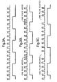
- Fig. 3 is a waveform chart illustrating the operation of the digital PLL of Fig. 2.
- Fig. 3A shows the output waveform after dividing the waveform of standard drive clock Rf 0 in a case where no control is performed.
- Fig. 3B shows the addition of 1 pulse to R-stage frequency dividing standard drive clock Rf 0 in a case where pulse addition is effected, and the output waveform after R-stage frequency division. By adding pulses in this way, output frequency following R-stage frequency dividing can be set to a high level.
- Fig. 3C shows the elimination of 1 pulse from R-stage frequency dividing standard drive clock Rf 0 in a case where pulse elimination is performed, and the output waveform after R-stage frequency division. By eliminating pulses in this way, output frequency following R-stage frequency division can be set to a low level.
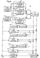
- Fig. 4 is a block schematic diagram of an N-order digital PLL including the digital PLL of Fig. 2.
- This N-order digital PLL is made up of first N-stage frequency divider 1, second N-stage frequency divider 2, multilevel quantized phase comparators 3-1, 3-2, ..., and 3-M, N1 counter 5, N2 counter 10-1, N3 counter 10-2, ..., and NN counter 10-(N-1), frequency regulator 6, R-stage frequency divider 7, Q 1 counter 8-1, Q 2 counter 8-2, ..., and Q N-1 counter 8-(N-1) that store the center frequencies of N2 counter 10-1, N3 counter 10-2, ..., and NN counter 10-(N-1), respectively, and rate multiplier 9-1, rate multiplier 9-2, ..., and rate multiplier 9-(N-1) that generate increment pulses or decrement pulses appropriate to the center frequency of the system.
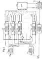
- a digital PLL which includes the provision, in the embodiment of Fig. 2, of N1 counters 5-1, 5-2, ..., and 5-M immediately after counters 5-1, 5-2, ..., and 5-M immediately after multilevel quantized phase comparators 3-1, 3-2, ..., and 3-M, respectively, and providing adder 4' immediately after N1 counter 5-1, 5-2, ..., and 5-M.
- N1 counters 5-1, 5-2, ..., and 5-M are competitive counters that input either advanced pulses indicating phase advance or delayed pulses indicating phase delay which are outputted by the corresponding multilevel quantized phase comparators 3-1, 3-2, ..., and 3-M, count up in response to the advanced pulses, and upon counting up to 2N1, both output an increment pulse and undergo setting to initial value N1.
- the N1 counters 5-1, 5-2, ..., and 5-M count down, and upon counting down to "0,” both output a decrement pulse and undergo setting to initial value N1.
- Adder 4 adds the increment pulses or decrement pulses of the M N1 counters 5-1 to 5-M and output pulses of an advanced phase or a delayed phase.
- the operation of this embodiment is otherwise similar to that of Fig. 2.
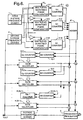
- Fig. 6 is a block schematic diagram showing an N-order digital PLL that includes the digital PLL of Fig. 5.
Landscapes
- Engineering & Computer Science (AREA)
- Multimedia (AREA)
- Computer Hardware Design (AREA)
- Computer Networks & Wireless Communication (AREA)
- Signal Processing (AREA)
- Stabilization Of Oscillater, Synchronisation, Frequency Synthesizers (AREA)
Claims (4)
- Digitaler Phasenregelkreis (PLL) mit
einer ersten N-stufigen Frequenzteilungseinrichtung (1), die Eingangstakte eines digitalen PLL einer N-stufigen Frequenzteilung unterzieht und N Takte einer ersten Phase, einer zweiten Phase, ... und einer N-ten Phase erzeugt, die mit einem ersten, zweiten Eingangstakt, ... bzw. N-ten Eingangstakt synchronisiert sind, diese N Takte in M Gruppen (N>M) teilt und das Ergebnis ausgibt;
einer zweiten N-stufigen Frequenzteilungseinrichtung (2), die Ausgangstakte eines digitalen PLL einer N-stufigen Frequenzteilung unterzieht, N Takte einer ersten, zweiten, ... und N-ten Phase erzeugt, die mit einem ersten, zweiten, ... bzw. N-ten Ausgangstakt synchronisiert sind, diese N Takte in M Gruppen (N>M) teilt und das Ergebnis ausgibt;
einer ersten mehrstufigen quantisierten Phasenvergleichseinrichtung (3-1), die ein beliebiges Ausgangssignal einer ersten Gruppe von ersten N-stufigen Frequenzteilungseinrichtungen (1) und ein beliebiges Ausgangssignal einer ersten Gruppe von zweiten N-stufigen Frequenzteilungseinrichtungen (2) aufnimmt und die Phasendifferenz zwischen den beiden Signalen als Wert ausgibt, der in mehreren Stufen quantisiert ist, einer zweiten mehrstufigen Phasenvergleichseinrichtung (3-2), die ein beliebiges Ausgangssignal einer zweiten Gruppe von ersten N-stufigen Frequenzteilungseinrichtungen (1) und ein beliebiges Ausgangssignal einer zweiten Gruppe von zweiten N-stufigen Frequenzteilungseinrichtungen (2) aufnimmt und eine Phasendifferenz zwischen den beiden Signalen als Wert ausgibt, die in mehreren Stufen quantisiert ist, ... und einer M-ten mehrstufigen quantisierten Phasenvergleichseinrichtung, die ein beliebiges Ausgangssignal einer M-ten Gruppe von ersten N-stufigen Frequenzteilungseinrichtungen (1) und ein beliebiges Ausgangssignal einer M-ten Gruppe von zweiten N-stufigen Frequenzteilungseinrichtungen (2) aufnimmt und eine Phasendifferenz zwischen den beiden Signalen als Wert ausgibt, der in mehreren Stufen quantisiert ist;
einer Addiereinrichtung (4), die Phasendifferenzinformation addiert, die von den mehrstufigen quantisierten Phasenvergleichseinrichtungen (3-1 ... 3-M) ausgegeben wird, und voreilende Impulse, die einen Phasenvorlauf anzeigen, oder verzögerte Impulse, die eine Phasenverzögerung anzeigen, ausgibt;
einer N1-Zähleinrichtung (5), die ein kompetitiver Zähler ist, der die voreilenden Impulse oder die verzögerten Impulse aufnimmt, als Antwort auf die voreilenden Impulse vorwärts zählt und beim Vorwärtszählen bis zum Zählwert 2N1 einen Inkrementimpuls ausgibt und auf den Anfangswert N1 gesetzt wird; und als Antwort auf die verzögerten Impulse rückwärts zählt und beim Rückwärtszählen bis "0" einen Dekrementimpuls ausgibt und auf den Anfangswert N1 gesetzt wird;
einer Frequenzregelungseinrichtung (6), die durch einen Standardsteuertakt (Rfo) des digitalen PLL gesteuert wird, einen Impuls aus der Impulsfolge des Standardsteuertaktes. (Rfo) beseitigt, wenn ein Inkrementimpuls von der N1-Zähleinrichtung (5) erzeugt wird, und der Impulsfolge des Standardsteuertaktes (Rfo) einen Impuls hinzufügt, wenn ein Dekrementimpuls von der N1-Zähleinricht (5) erzeugt wird; und
einer R-stufigen Frequenzteilungseinrichtung (7), die ein Ausgangssignal der Frequenzregelungseinrichtung (6) einer R-stufigen Frequenzteilung unterzieht und den Ausgangstakt des digitalen PLL ausgibt;
wobei von den M mehrstufigen quantisierten Phasenvergleichseinrichtungen (3-1 ... 3-M) mehrstufige quantisierte Phasenvergleichseinrichtungen ungeradzahliger Ordnungszahlen durch einen Phasenzähltakt einer positiven Phase gesteuert werden und mehrstufige quantisierte Phasenvergleichseinrichtungen geradzahliger Ordnungszahlen durch einen Phasenzähltakt einer negativen Phase gesteuert werden. - Digitaler PLL N-ter Ordnung mit einem digitalen PLL nach Anspruch 1.
- Digitaler PLL mit
einer ersten N-stufigen Frequenzteilungseinrichtung (1), die Eingangstakte eines digitalen PLL einer N-stufigen Frequenzteilung unterzieht, N Takte einer ersten, zweiten, ... und N-ten Phase teilt, die mit einem ersten, zweiten, ... bzw. N-ten Eingangstakt synchronisiert sind, diese N Takte in M Gruppen (N>M) teilt und das Ergebnis ausgibt;
einer zweiten N-stufigen Frequenzteilungseinrichtung (2), die Ausgangstakte eines digitalen PLL einer N-stufigen Frequenzteilung unterzieht, N Takte einer ersten, zweiten, ... und N-ten Phase erzeugt, die mit einem ersten, zweiten, ... bzw. N-ten Ausgangstakt synchronisiert sind, diese N Takte in M Gruppen (N>M) teilt und das Ergebnis ausgibt;
einer ersten mehrstufigen quantisierten Phasenvergleichseinrichtung (3-1), die ein beliebiges Ausgangssignal einer ersten Gruppe von ersten N-stufigen Frequenzteilungseinrichtungen (1) und ein beliebiges Ausgangssignal einer ersten Gruppe von zweiten Frequenzteilungseinrichtungen (2) aufnimmt und eine Phasendifferenz zwischen den beiden Signalen in Form von voreilenden Impulsen, die einen Phasenvorlauf anzeigen, oder von verzögerten Impulsen, die eine Phasenverzögerung anzeigen, als Wert ausgibt, der in mehreren Stufen quantisiert ist; einer zweiten mehrstufigen quantisierten Phasenvergleichseinrichtung (3-2), die ein beliebiges Ausgangssignal einer zweiten Gruppe von ersten N-stufigen Frequenzteilungseinrichtungen (1) und ein beliebiges Ausgangssignal einer zweiten Gruppe von zweiten N-stufigen Frequenzteilungseinrichtungen (2) aufnimmt und eine Phasendifferenz zwischen den beiden Signalen als Wert ausgibt, der in mehreren Stufen quantisiert ist; ...; und einer M-ten mehrstufigen quantisierten Phasenvergleichseinrichtung (3M), die ein beliebiges Ausgangssignal einer M-ten Gruppe von ersten N-stufigen Frequenzteilungseinrichtungen (1) und ein beliebiges Ausgangssignal einer M-ten Gruppe von zweiten N-stufigen Frequenzteilungseinrichtungen (2) aufnimmt und eine Phasendifferenz zwischen den beiden Signalen als Wert ausgibt, der in mehreren Stufen quantisiert ist;
N1-Zähleinrichtungen (5-1, 5-2, ... 5-M), die kompetitive Zähler sind, die entsprechend jeder der M mehrstufigen quantisierten Phasenvergleichseinrichtungen (3-1, 3-2, ... 3-M) bereitgestellt werden und die die voreilenden Impulse, die einen Phasenvorlauf anzeigen, oder die verzögerten Impulse, die eine Phasenverzögerung anzeigen, aufnehmen, die von den jeweiligen mehrstufigen quantisierten Phasenvergleichseinrichtungen (3-1, 3-2 ... 3-M) ausgegeben werden, als Antwort auf die voreilenden Impulse vorwärts zählen und beim Vorwärtszählen bis zum Zählwert 2N1 einen Inkrementimpuls ausgeben und auf den Anfangswert N1 zurückgesetzt werden; und als Antwort auf die verzögerten Impulse rückwärts zählen und beim Rückwärtszählen bis "0" einen Dekrementimpuls ausgeben und auf den Anfangswert N1 zurückgesetzt werden;
einer Addiereinrichtung (4), die Inkrementimpulse oder Dekrementimpulse der M N1-Zähleinrichtungen (5-1, 5-2, ... 5-M) addiert und Impulse einer voreilenden Phase oder einer verzögerten Phase ausgibt;
einer Frequenzregelungseinrichtung (6), die durch einen Standardsteuertakt (Rfo) eines digitalen PLL gesteuert wird, einen Impuls aus der Impulsfolge des Standardsteuertaktes beseitigt, wenn ein Impuls einer voreilenden Phase von der Addiereinrichtung (4) erzeugt wird, und der Impulsfolge des Standardsteuertaktes einen Impuls hinzufügt, wenn ein Impuls einer verzögerten Phase von der Addiereinrichtung erzeugt wird;
einer R-stufigen Frequenzteilungseinrichtung (7), die das Ausgangssignal der Frequenzregelungseinrichtung (6) einer R-stufigen Frequenzteilung unterzieht und einen Ausgangstakt des digitalen PLL ausgibt;
wobei von den M mehrstufigen quantisierten Phasenvergleichseinrichtungen (3-1, 3-2, ... 3-M) mehrstufige quantisierte Phasenvergleichseinrichtungen ungeradzahliger Ordnungszahlen durch einen Phasenzählertakt einer positiven Phase gesteuert werden und mehrstufige quantisierte Phasenvergleichseinrichtungen geradzahliger Ordnungszahlen durch einen Phasenzähltakt einer negativen Phase gesteuert werden. - Digitaler PLL N-ter Ordnung mit einem digitalen PLL nach Anspruch 3.
Applications Claiming Priority (3)
| Application Number | Priority Date | Filing Date | Title |
|---|---|---|---|
| JP105933/95 | 1995-04-28 | ||
| JP10593395 | 1995-04-28 | ||
| JP7105933A JP2964912B2 (ja) | 1995-04-28 | 1995-04-28 | デジタルpll |
Publications (3)
| Publication Number | Publication Date |
|---|---|
| EP0740423A2 EP0740423A2 (de) | 1996-10-30 |
| EP0740423A3 EP0740423A3 (de) | 1998-04-08 |
| EP0740423B1 true EP0740423B1 (de) | 2003-07-23 |
Family
ID=14420660
Family Applications (1)
| Application Number | Title | Priority Date | Filing Date |
|---|---|---|---|
| EP96302922A Expired - Lifetime EP0740423B1 (de) | 1995-04-28 | 1996-04-26 | Digitaler Phasenregelkreis |
Country Status (5)
| Country | Link |
|---|---|
| US (1) | US5694068A (de) |
| EP (1) | EP0740423B1 (de) |
| JP (1) | JP2964912B2 (de) |
| CA (1) | CA2175133C (de) |
| DE (1) | DE69629147T2 (de) |
Families Citing this family (21)
| Publication number | Priority date | Publication date | Assignee | Title |
|---|---|---|---|---|
| JP3086706B2 (ja) * | 1995-08-03 | 2000-09-11 | アンリツ株式会社 | ラショナル分周装置及びそれを用いる周波数シンセサイザ |
| US6021503A (en) * | 1996-12-21 | 2000-02-01 | Micron Communications, Inc. | Bit synchronization for interrogator |
| US6223317B1 (en) * | 1998-02-28 | 2001-04-24 | Micron Technology, Inc. | Bit synchronizers and methods of synchronizing and calculating error |
| US6959062B1 (en) | 2000-01-28 | 2005-10-25 | Micron Technology, Inc. | Variable delay line |
| US7170963B2 (en) * | 2003-01-15 | 2007-01-30 | Nano Silicon Pte. Ltd. | Clock recovery method by phase selection |
| JP3803805B2 (ja) * | 2003-09-05 | 2006-08-02 | 日本テキサス・インスツルメンツ株式会社 | ディジタル位相同期ループ回路 |
| WO2011150964A1 (en) * | 2010-06-01 | 2011-12-08 | Abb Technology Ag | Precision switching for carrier based pwm |
| CN115085727B (zh) | 2016-04-22 | 2026-04-21 | 康杜实验室公司 | 高性能锁相环 |
| US10193716B2 (en) | 2016-04-28 | 2019-01-29 | Kandou Labs, S.A. | Clock data recovery with decision feedback equalization |
| US10411922B2 (en) | 2016-09-16 | 2019-09-10 | Kandou Labs, S.A. | Data-driven phase detector element for phase locked loops |
| US10200188B2 (en) | 2016-10-21 | 2019-02-05 | Kandou Labs, S.A. | Quadrature and duty cycle error correction in matrix phase lock loop |
| CN110945830B (zh) | 2017-05-22 | 2022-09-09 | 康杜实验室公司 | 多模式数据驱动型时钟恢复电路 |
| CN107911114B (zh) * | 2017-11-15 | 2021-03-09 | 中国科学技术大学 | 一种恒定环路带宽的宽带锁相环 |
| US10554380B2 (en) | 2018-01-26 | 2020-02-04 | Kandou Labs, S.A. | Dynamically weighted exclusive or gate having weighted output segments for phase detection and phase interpolation |
| EP4145705A1 (de) | 2018-06-12 | 2023-03-08 | Kandou Labs SA | Kombiniertes taktdatenrückgewinnungslogiknetzwerk und ladungspumpenschaltung mit niedriger latenzzeit |
| US10630272B1 (en) | 2019-04-08 | 2020-04-21 | Kandou Labs, S.A. | Measurement and correction of multiphase clock duty cycle and skew |
| US10673443B1 (en) | 2019-04-08 | 2020-06-02 | Kandou Labs, S.A. | Multi-ring cross-coupled voltage-controlled oscillator |
| US10958251B2 (en) | 2019-04-08 | 2021-03-23 | Kandou Labs, S.A. | Multiple adjacent slicewise layout of voltage-controlled oscillator |
| US11463092B1 (en) | 2021-04-01 | 2022-10-04 | Kanou Labs Sa | Clock and data recovery lock detection circuit for verifying lock condition in presence of imbalanced early to late vote ratios |
| US11563605B2 (en) | 2021-04-07 | 2023-01-24 | Kandou Labs SA | Horizontal centering of sampling point using multiple vertical voltage measurements |
| US11496282B1 (en) | 2021-06-04 | 2022-11-08 | Kandou Labs, S.A. | Horizontal centering of sampling point using vertical vernier |
Family Cites Families (5)
| Publication number | Priority date | Publication date | Assignee | Title |
|---|---|---|---|---|
| US4808884A (en) * | 1985-12-02 | 1989-02-28 | Western Digital Corporation | High order digital phase-locked loop system |
| JP2993200B2 (ja) * | 1991-07-31 | 1999-12-20 | 日本電気株式会社 | 位相同期ループ |
| FR2682236B1 (fr) * | 1991-10-04 | 1997-01-03 | Cit Alcatel | Procede et dispositif de commande de mode de fonctionnement d'une boucle a verrouillage de phase numerique |
| JP3232351B2 (ja) * | 1993-10-06 | 2001-11-26 | 三菱電機株式会社 | デジタル回路装置 |
| US5463351A (en) * | 1994-09-29 | 1995-10-31 | Motorola, Inc. | Nested digital phase lock loop |
-
1995
- 1995-04-28 JP JP7105933A patent/JP2964912B2/ja not_active Expired - Fee Related
-
1996
- 1996-04-25 US US08/637,608 patent/US5694068A/en not_active Expired - Lifetime
- 1996-04-26 CA CA002175133A patent/CA2175133C/en not_active Expired - Fee Related
- 1996-04-26 DE DE69629147T patent/DE69629147T2/de not_active Expired - Lifetime
- 1996-04-26 EP EP96302922A patent/EP0740423B1/de not_active Expired - Lifetime
Also Published As
| Publication number | Publication date |
|---|---|
| US5694068A (en) | 1997-12-02 |
| EP0740423A2 (de) | 1996-10-30 |
| JP2964912B2 (ja) | 1999-10-18 |
| JPH08307250A (ja) | 1996-11-22 |
| DE69629147T2 (de) | 2004-02-19 |
| DE69629147D1 (de) | 2003-08-28 |
| CA2175133C (en) | 2000-04-04 |
| CA2175133A1 (en) | 1996-10-29 |
| EP0740423A3 (de) | 1998-04-08 |
Similar Documents
| Publication | Publication Date | Title |
|---|---|---|
| EP0740423B1 (de) | Digitaler Phasenregelkreis | |
| US4339722A (en) | Digital frequency multiplier | |
| US4574243A (en) | Multiple frequency digital phase locked loop | |
| US20020008557A1 (en) | Reduced jitter phase lock loop using a technique multi-stage digital delay line | |
| US5105160A (en) | Phase comparator using digital and analogue phase detectors | |
| US5737373A (en) | Control method and apparatus for suppressing jitter | |
| US4617520A (en) | Digital lock detector for a phase-locked loop | |
| EP2153523A1 (de) | Frequenzsynchronisation | |
| US6757349B1 (en) | PLL frequency synthesizer with lock detection circuit | |
| EP0757445A2 (de) | Frequenzsynthetisierer mit einem Phasenregelkreis | |
| EP0670635B1 (de) | PLL-Oszillator, Schaltung zur fortlaufenden Mittelwertbildung sowie Teilerverhältnis-Entzerrerschaltung | |
| US5126693A (en) | Circuit and method of reducing phase jitter in a phase lock loop | |
| US6064241A (en) | Direct digital frequency synthesizer using pulse gap shifting technique | |
| US5241285A (en) | Phase locked loop reference slaving circuit | |
| US4628519A (en) | Digital phase-locked loop circuit | |
| EP0168426B1 (de) | Digitale phasenriegelschleife für multiple frequenzen | |
| US6316973B1 (en) | Transmission timing adjusting circuit and method | |
| EP1502180A2 (de) | Vorrichtung und verfahren für taktlose datenrückgewinnung | |
| US4691327A (en) | Clock regenerator | |
| JPH1079645A (ja) | 周波数選択装置及びそれに設けられた同期検出器 | |
| JPH0884071A (ja) | 完全2次系dpllおよびそれを用いたデスタッフ回路 | |
| EP1514371B1 (de) | Rahmengrenzenunterscheider | |
| EP0966103B1 (de) | Frequenzsynthetisierer | |
| US6333651B1 (en) | Second order digital jitter attenuator | |
| JPS6320051B2 (de) |
Legal Events
| Date | Code | Title | Description |
|---|---|---|---|
| PUAI | Public reference made under article 153(3) epc to a published international application that has entered the european phase |
Free format text: ORIGINAL CODE: 0009012 |
|
| AK | Designated contracting states |
Kind code of ref document: A2 Designated state(s): DE FR GB NL |
|
| PUAL | Search report despatched |
Free format text: ORIGINAL CODE: 0009013 |
|
| AK | Designated contracting states |
Kind code of ref document: A3 Designated state(s): DE FR GB NL |
|
| 17P | Request for examination filed |
Effective date: 19980320 |
|
| 17Q | First examination report despatched |
Effective date: 20010611 |
|
| GRAH | Despatch of communication of intention to grant a patent |
Free format text: ORIGINAL CODE: EPIDOS IGRA |
|
| GRAH | Despatch of communication of intention to grant a patent |
Free format text: ORIGINAL CODE: EPIDOS IGRA |
|
| GRAA | (expected) grant |
Free format text: ORIGINAL CODE: 0009210 |
|
| AK | Designated contracting states |
Designated state(s): DE FR GB NL |
|
| REG | Reference to a national code |
Ref country code: GB Ref legal event code: FG4D |
|
| REF | Corresponds to: |
Ref document number: 69629147 Country of ref document: DE Date of ref document: 20030828 Kind code of ref document: P |
|
| ET | Fr: translation filed | ||
| PLBE | No opposition filed within time limit |
Free format text: ORIGINAL CODE: 0009261 |
|
| STAA | Information on the status of an ep patent application or granted ep patent |
Free format text: STATUS: NO OPPOSITION FILED WITHIN TIME LIMIT |
|
| 26N | No opposition filed |
Effective date: 20040426 |
|
| PGFP | Annual fee paid to national office [announced via postgrant information from national office to epo] |
Ref country code: NL Payment date: 20090427 Year of fee payment: 14 Ref country code: FR Payment date: 20090417 Year of fee payment: 14 |
|
| REG | Reference to a national code |
Ref country code: NL Ref legal event code: V1 Effective date: 20101101 |
|
| REG | Reference to a national code |
Ref country code: FR Ref legal event code: ST Effective date: 20101230 |
|
| PG25 | Lapsed in a contracting state [announced via postgrant information from national office to epo] |
Ref country code: NL Free format text: LAPSE BECAUSE OF NON-PAYMENT OF DUE FEES Effective date: 20101101 |
|
| PG25 | Lapsed in a contracting state [announced via postgrant information from national office to epo] |
Ref country code: FR Free format text: LAPSE BECAUSE OF NON-PAYMENT OF DUE FEES Effective date: 20100430 |
|
| PGFP | Annual fee paid to national office [announced via postgrant information from national office to epo] |
Ref country code: DE Payment date: 20130508 Year of fee payment: 18 Ref country code: GB Payment date: 20130424 Year of fee payment: 18 |
|
| REG | Reference to a national code |
Ref country code: DE Ref legal event code: R119 Ref document number: 69629147 Country of ref document: DE |
|
| GBPC | Gb: european patent ceased through non-payment of renewal fee |
Effective date: 20140426 |
|
| REG | Reference to a national code |
Ref country code: DE Ref legal event code: R119 Ref document number: 69629147 Country of ref document: DE Effective date: 20141101 |
|
| PG25 | Lapsed in a contracting state [announced via postgrant information from national office to epo] |
Ref country code: DE Free format text: LAPSE BECAUSE OF NON-PAYMENT OF DUE FEES Effective date: 20141101 Ref country code: GB Free format text: LAPSE BECAUSE OF NON-PAYMENT OF DUE FEES Effective date: 20140426 |