EP0740425A1 - Genauigkeits-Digital-Analog-Wandler - Google Patents
Genauigkeits-Digital-Analog-Wandler Download PDFInfo
- Publication number
- EP0740425A1 EP0740425A1 EP96410037A EP96410037A EP0740425A1 EP 0740425 A1 EP0740425 A1 EP 0740425A1 EP 96410037 A EP96410037 A EP 96410037A EP 96410037 A EP96410037 A EP 96410037A EP 0740425 A1 EP0740425 A1 EP 0740425A1
- Authority
- EP
- European Patent Office
- Prior art keywords
- transistors
- voltage
- transistor
- vout
- current
- Prior art date
- Legal status (The legal status is an assumption and is not a legal conclusion. Google has not performed a legal analysis and makes no representation as to the accuracy of the status listed.)
- Granted
Links
- 108090000699 N-Type Calcium Channels Proteins 0.000 abstract 1
- 102000004129 N-Type Calcium Channels Human genes 0.000 abstract 1
- 108010075750 P-Type Calcium Channels Proteins 0.000 abstract 1
- 238000000034 method Methods 0.000 description 6
- 230000007423 decrease Effects 0.000 description 5
- 238000006243 chemical reaction Methods 0.000 description 2
- 230000000295 complement effect Effects 0.000 description 2
- 230000000694 effects Effects 0.000 description 2
- 238000012935 Averaging Methods 0.000 description 1
- 230000007547 defect Effects 0.000 description 1
- 230000004048 modification Effects 0.000 description 1
- 238000012986 modification Methods 0.000 description 1
- 230000001105 regulatory effect Effects 0.000 description 1
- 238000005070 sampling Methods 0.000 description 1
- 230000035945 sensitivity Effects 0.000 description 1
Images

Classifications
-
- H—ELECTRICITY
- H03—ELECTRONIC CIRCUITRY
- H03M—CODING; DECODING; CODE CONVERSION IN GENERAL
- H03M1/00—Analogue/digital conversion; Digital/analogue conversion
- H03M1/66—Digital/analogue converters
- H03M1/74—Simultaneous conversion
- H03M1/742—Simultaneous conversion using current sources as quantisation value generators
- H03M1/745—Simultaneous conversion using current sources as quantisation value generators with weighted currents
Definitions
- the present invention relates to precision digital / analog converters, such as those used in the reproduction of the sound recorded on laser discs.
- a battery of current sources is commonly used which are connected in greater or lesser number on a common output line as a function of digital data. Given the inevitable pairing faults between the current sources, the precision obtained by this method cannot exceed 10 bits.
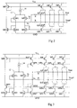
- FIG. 1 schematically illustrates a digital / analog converter making it possible to obtain a higher precision, described in an article of IEEE Journal of Solid-State Circuits, vol. 16, No. 12, December 1991, entitled "An Oversampled Multibit CMOS D / A Converter for Digital Audio with 115-dB Dynamic Range".
- This converter includes a battery of positive current sources IP1 to IPn and a battery of negative current sources IN1 to INn.
- a digital control signal C selects the positive or negative current sources to be connected in a complementary manner to two differential output lines Iout and Iout *. Operating in differential mode improves certain characteristics, such as noise sensitivity.
- the current sources IP and IN have the same value I, and they are generally switched so that they are always connected to one or the other of the lines Iout and Iout *, to avoid switching noise.
- each IP source is periodically calibrated to an IPc calibration source, and each IN source is periodically calibrated to an INc calibration source.
- the value of an IP or IN source is kept between two calibrations by capacitive effect. It is thus ensured that the value of each of the IP sources is equal to the value of the calibration source IPc and that the value of each of the sources IN is equal to the value of the calibration source INc.
- the lines Iout and Iout * vary symmetrically with respect to each other.
- the value of the IN sources must be equal to the value of the IP sources, or that the value of the IPc calibration source is equal to the value of the INc calibration source.
- the batteries of IP and IN sources each include an additional source, respectively IPs and INs connected to each other.
- the current difference between the sources IPs and INs is taken by an integrator 10, the output of which readjusts the value of the calibration source INc until the currents of the sources IPs and INs are equal.
- the quality of this symmetry setting depends on the pairing of the IPs source with each of the IP sources and on the pairing of the INs source with each of the IN sources. Given the large number of sources, matching is particularly difficult.
- An object of the present invention is to provide a precision digital / analog converter in which the adjustment of the symmetry is particularly precise.
- a digital / analog converter comprising pairs of positive and negative current sources connected by switches with two differential output lines, the switches being controlled as a function of digital data.
- Each pair of current sources is a pair of transistors of an output stage of a transconductance amplifier receiving a reference voltage on a non-inverting input and, on its inverting input, the voltage at the midpoint of a bridge. of resistors connected between the differential lines, the converter output being the voltage between the two differential lines.
- the transconductance amplifier comprises a differential stage, the current in a first branch of this differential stage being copied into first transistors of the pairs of transistors and the current of a second branch of l 'differential stage being copied into the second transistors of the pairs of transistors.
- the transistors of the couples of the transistors are connected to respective cascode transistors, polarized with respect to the voltage at the midpoint of the resistance bridge.
- a battery of positive current sources is constituted by P channel MP MP MOS transistors connected in parallel by their sources and their gates, the sources being connected to a high supply voltage Vcc.
- a complementary battery of negative current sources is constituted by N-channel MOS transistors MN connected in parallel by their sources and their gates, the sources being connected to a low supply potential GND.
- the drain of each of the transistors MP is connected to two differential output lines Vout and Vout * by two respective switches KP and KP *.
- the drain of each of the transistors MN is connected to the lines Vout and Vout * by two respective switches KN and KN *.
- the transistors MP and MN form an output stage of a transconductance amplifier.
- This amplifier comprises a differential input stage 12 formed, for example, of two P-channel MOS transistors MP1 and MP2, the sources of which are connected to the potential Vcc by a source of quiescent current 14.
- the drain current of the transistor MP1, forming a first branch of stage 12 is copied into each of the transistors MP by a first current mirror circuit.
- the drain current of the transistor MP2, forming a second branch of the stage 12 is copied into each of the transistors MN by a second current mirror circuit.
- the first current mirror circuit comprises an N-channel MOS transistor MN3 whose drain and gate are connected to the drain of transistor MP1, and whose source is connected GND potential.
- An N-channel MOS transistor MN4 is connected in parallel to the transistor MN3 by its gate and its source and forms with the transistor MN3 a current mirror which copies the current from the transistor MP1 into the transistor MN4.
- the drain of this transistor MN4 is connected to the drain and to the gate of a P-channel MOS transistor MP5 whose source is connected to the potential Vcc.
- this transistor MP5 is connected in parallel by its gate and its source on the transistors MP.
- the transistors MP5 and MP form a current mirror which copies in each of the transistors MP the drain current of the transistor MN4, and therefore of the transistor MP1.
- the second current mirror circuit comprises an N-channel MOS transistor MN6, the drain and the gate of which are connected to the drain of the transistor MP2.
- this transistor MN6 is connected in parallel by its gate and its source to the transistors MN and forms with these a current mirror which copies in each of the transistors MN the drain current of the transistor MP2.
- the gate of transistor MP1 constitutes an inverting input of the transconductance amplifier, and the gate of transistor MP2 constitutes a non-inverting input.
- the gate of the transistor MP1 receives the voltage Vc present at the midpoint of a resistor bridge R of the same value connected between the differential output lines Vout and Vout *.
- the output of the converter according to the invention is the differential voltage present at the terminals of the resistance bridge R (or between the lines Vout and Vout *).
- the gate of the transistor MP2 receives a reference voltage Vr, which is the voltage with respect to which the output of the converter must be symmetrical.
- the voltage Vc is regulated on the voltage of reference Vr, which ensures the symmetry of the voltage between the lines Vout and Vout * with respect to the voltage Vr, regardless of the number of MP or MN sources connected to the lines Vout and Vout *, provided that at least one MP source is connected to one of the lines Vout and Vout * and at least one source MN to the other of the lines.
- the current of the transistor MP1 decreases.
- the conductance of the transistors MP decreases, which causes the voltage Vc to decrease.
- the current of the transistor MP2 increases symmetrically with the decrease of the current of the transistor MP1.
- the conductance of the transistors MN increases, which also tends to decrease the voltage Vc.
- this circuit effectively tends to restore the equilibrium point where the voltage Vc is equal to the reference voltage Vr.
- the symmetry of the output signal that is to say the differential voltage between the lines Vout and Vout *, depends only on the ratio of the resistors R. The pairing of only two resistors can be carried out in a particularly precise way, since the resistors R can be integrated very close to each other.
- a converter according to the invention is particularly well suited to a particular method of switching the MP and MN transistors making it possible to obtain the desired precision, this method being notably simpler to implement and as precise as the self-calibration method. described in relation to Figure 1.
- This is a so-called "butterfly" switching method.
- this method consists in choosing, at each switching, a pseudo-random combination of m transistors MP and m transistors MN among the set of transistors that one can choose.
- the best results are obtained if these switching operations are carried out at a frequency clearly greater than the sampling frequency of the digital data to be converted.
- FIG. 3 represents a modification of the converter of FIG. 2, intended to make the converter less sensitive to variations in its supply voltage.
- Each of the transistors MP is connected to its switches KP and KP * via a cascode transistor with P channel MPc.
- each of the transistors MN is connected to its switches KN and KN * via an N-channel cascode transistor MNc.
- the amplifier includes an additional output stage intended to polarize the cascode transistors MPc and MNc. This additional stage comprises a P-channel MOS transistor MP7 connected in parallel by its gate and its source on the MP transistors and an N-channel MOS transistor MN7 connected in parallel by its gate and its source on the MN transistors.
- the drain of the transistor MP7 is connected to the midpoint of the resistance bridge R by a P-channel MOS transistor MP8, the drain and the gate of which are connected to the gates of the transistors MPc.
- the transistor MN7 is connected to the midpoint of the resistance bridge R by an N-channel MOS transistor MN8, the drain and the gate of which are connected to the gates of the transistors MNc.
- the drain potential of the transistors MP is fixed at the potential Vc increased by the threshold voltage of the transistors MPc, and the drain potential of the transistors MN is fixed at the potential Vc reduced by the threshold voltage of the transistors MNc.
- the peak voltage on the output Vout or Vout * is thus limited to the threshold voltage of a transistor MPc or MNc, which is sufficient.
- the additional output stage comprising the transistors MP7 and MN7 operates under the same conditions as the output stage formed by the transistors MP and MN, and does not inject in principle no current in the resistors R. However, if there is a symmetry defect on the output stage comprising the transistors MP and MN, the additional stage absorbs a residual current through the resistors R, which contributes to compensate for the lack of symmetry.
- An additional N-channel cascode transistor MN9 is disposed between the transistors MN4 and MP5 and its gate is connected to the gates of the transistors MNc.
- This cascode transistor makes it possible to operate the current mirror MN3 / MN4 under the same conditions as the current mirror MN6 / MN, which contributes to improving the symmetry.
Landscapes
- Engineering & Computer Science (AREA)
- Theoretical Computer Science (AREA)
- Analogue/Digital Conversion (AREA)
Applications Claiming Priority (2)
| Application Number | Priority Date | Filing Date | Title |
|---|---|---|---|
| FR9505367 | 1995-04-28 | ||
| FR9505367A FR2733650B1 (fr) | 1995-04-28 | 1995-04-28 | Convertisseur numerique/analogique de precision |
Publications (2)
| Publication Number | Publication Date |
|---|---|
| EP0740425A1 true EP0740425A1 (de) | 1996-10-30 |
| EP0740425B1 EP0740425B1 (de) | 2001-08-01 |
Family
ID=9478718
Family Applications (1)
| Application Number | Title | Priority Date | Filing Date |
|---|---|---|---|
| EP96410037A Expired - Lifetime EP0740425B1 (de) | 1995-04-28 | 1996-04-24 | Genauigkeits-Digital-Analog-Wandler |
Country Status (5)
| Country | Link |
|---|---|
| US (1) | US5815103A (de) |
| EP (1) | EP0740425B1 (de) |
| JP (1) | JP2930005B2 (de) |
| DE (1) | DE69614181D1 (de) |
| FR (1) | FR2733650B1 (de) |
Cited By (2)
| Publication number | Priority date | Publication date | Assignee | Title |
|---|---|---|---|---|
| WO1998020616A1 (en) * | 1996-11-04 | 1998-05-14 | Telefonaktiebolaget Lm Ericsson (Publ) | A method and device to provide a high-performance digital-to-analog conversion architecture |
| KR100487495B1 (ko) * | 1997-08-26 | 2005-08-24 | 삼성전자주식회사 | 디지털-아날로그변환기 |
Families Citing this family (20)
| Publication number | Priority date | Publication date | Assignee | Title |
|---|---|---|---|---|
| FR2768852B1 (fr) * | 1997-09-22 | 1999-11-26 | Sgs Thomson Microelectronics | Realisation d'un condensateur intermetallique |
| JP4001421B2 (ja) * | 1998-07-23 | 2007-10-31 | 沖電気工業株式会社 | Da変換器 |
| US6150970A (en) * | 1999-03-01 | 2000-11-21 | Sony Corporation | Method and system for digital to analog conversion |
| US6317069B1 (en) * | 1999-05-06 | 2001-11-13 | Texas Instruments Incorporated | Digital-to-analog converter employing binary-weighted transistor array |
| US6278393B1 (en) * | 1999-08-12 | 2001-08-21 | Agere Systems Guardian Corp. | Multiple output digital-to-analog converter |
| US6295012B1 (en) | 1999-08-25 | 2001-09-25 | Broadcom Corporation | CMOS DAC with high impedance differential current drivers |
| DE10038372C2 (de) * | 2000-08-07 | 2003-03-13 | Infineon Technologies Ag | Differentieller Digital/Analog-Wandler |
| DE10053914C2 (de) * | 2000-10-31 | 2003-05-22 | Infineon Technologies Ag | Digital/Analog-Wandler mit programmierbarer Verstärkung |
| US6809673B2 (en) * | 2001-10-10 | 2004-10-26 | Analog Devices, Inc. | Multi-channel circuit with current steering digital to analogue converters with minimized crosstalk |
| JP3820375B2 (ja) * | 2002-02-14 | 2006-09-13 | フリースケール セミコンダクター インコーポレイテッド | デジタル・アナログ変換回路 |
| US6621432B1 (en) * | 2002-09-03 | 2003-09-16 | Cirrus Logic, Inc. | Digital to differential converters and digital to analog converters using the same |
| US6750797B1 (en) * | 2003-01-31 | 2004-06-15 | Inovys Corporation | Programmable precision current controlling apparatus |
| TWI274889B (en) * | 2005-10-06 | 2007-03-01 | Elan Microelectronics Corp | Resistive touch screen measurement system |
| US7903011B2 (en) * | 2006-09-13 | 2011-03-08 | Honeywell International Inc. | Differential current-mode translator in a sigma-delta digital-to-analog converter |
| JP2009194558A (ja) * | 2008-02-13 | 2009-08-27 | Toshiba Corp | カレントミラー回路及びデジタルアナログ変換回路 |
| US7956782B2 (en) * | 2009-06-11 | 2011-06-07 | Honeywell International Inc. | Current-mode sigma-delta digital-to-analog converter |
| US8519877B1 (en) * | 2012-03-28 | 2013-08-27 | Texas Instruments Incorporated | Low noise and low power arrangement for playing audio signals |
| KR20170000542A (ko) * | 2015-06-24 | 2017-01-03 | 삼성전자주식회사 | 플리커 노이즈를 저감하는 전류 dac 회로 |
| US9584151B1 (en) * | 2016-03-01 | 2017-02-28 | Analog Devices, Inc. | Randomized quad switching |
| US10009686B1 (en) * | 2017-04-17 | 2018-06-26 | Cirrus Logic, Inc. | Fully-differential current digital-to-analog converter |
Citations (1)
| Publication number | Priority date | Publication date | Assignee | Title |
|---|---|---|---|---|
| US4683458A (en) * | 1986-07-31 | 1987-07-28 | Robert Hallgren | Current-steering digital-to-analog converter for providing bi-directional currents through a load |
Family Cites Families (8)
| Publication number | Priority date | Publication date | Assignee | Title |
|---|---|---|---|---|
| US3924229A (en) * | 1969-01-10 | 1975-12-02 | Ibm | Bipolar digital to analog converter utilizing two reference voltages of the same polarity |
| US4616189A (en) * | 1985-04-26 | 1986-10-07 | Triquint Semiconductor, Inc. | Gallium arsenide differential amplifier with closed loop bias stabilization |
| US4605907A (en) * | 1985-05-20 | 1986-08-12 | Teledyne Industries, Inc. | Precisely adjustable voltage controlled current mirror amplifier |
| US4667165A (en) * | 1986-02-19 | 1987-05-19 | Advanced Micro Devices, Inc. | High-speed full differential amplifier with common mode rejection |
| US4904953A (en) * | 1988-04-22 | 1990-02-27 | Triquint Semiconductor, Inc. | Differential amplifier with common-mode bias feedback |
| JPH0832406A (ja) * | 1994-05-12 | 1996-02-02 | Hitachi Ltd | 電圧制御フィルタ回路及び信号処理用半導体集積回路装置並びにそれを用いた信号読み取りシステム |
| US5491448A (en) * | 1994-07-29 | 1996-02-13 | National Semiconductor Corporation | Class AB output stage with improved frequency stability |
| US5574678A (en) * | 1995-03-01 | 1996-11-12 | Lattice Semiconductor Corp. | Continuous time programmable analog block architecture |
-
1995
- 1995-04-28 FR FR9505367A patent/FR2733650B1/fr not_active Expired - Fee Related
-
1996
- 1996-04-16 US US08/634,306 patent/US5815103A/en not_active Expired - Lifetime
- 1996-04-24 EP EP96410037A patent/EP0740425B1/de not_active Expired - Lifetime
- 1996-04-24 DE DE69614181T patent/DE69614181D1/de not_active Expired - Lifetime
- 1996-04-26 JP JP8129255A patent/JP2930005B2/ja not_active Expired - Fee Related
Patent Citations (1)
| Publication number | Priority date | Publication date | Assignee | Title |
|---|---|---|---|---|
| US4683458A (en) * | 1986-07-31 | 1987-07-28 | Robert Hallgren | Current-steering digital-to-analog converter for providing bi-directional currents through a load |
Non-Patent Citations (1)
| Title |
|---|
| H.J.SCHOUWENAARS ET.AL.: "An Oversampled Multibit CMOS D/A Converter for Digital Audio with 115-dB Dynamic Range.", IEEE JOURNAL OF SOLID-STATE CIRCUITS, vol. 26, no. 12, pages 1775 - 1780, XP002010583 * |
Cited By (3)
| Publication number | Priority date | Publication date | Assignee | Title |
|---|---|---|---|---|
| US5933107A (en) * | 1996-04-11 | 1999-08-03 | Telefonaktiebolaget Lm Ericsson | Method and device to provide a high-performance digital-to-analog conversion architecture |
| WO1998020616A1 (en) * | 1996-11-04 | 1998-05-14 | Telefonaktiebolaget Lm Ericsson (Publ) | A method and device to provide a high-performance digital-to-analog conversion architecture |
| KR100487495B1 (ko) * | 1997-08-26 | 2005-08-24 | 삼성전자주식회사 | 디지털-아날로그변환기 |
Also Published As
| Publication number | Publication date |
|---|---|
| FR2733650A1 (fr) | 1996-10-31 |
| JP2930005B2 (ja) | 1999-08-03 |
| US5815103A (en) | 1998-09-29 |
| EP0740425B1 (de) | 2001-08-01 |
| JPH08307274A (ja) | 1996-11-22 |
| DE69614181D1 (de) | 2001-09-06 |
| FR2733650B1 (fr) | 1997-07-18 |
Similar Documents
| Publication | Publication Date | Title |
|---|---|---|
| EP0740425B1 (de) | Genauigkeits-Digital-Analog-Wandler | |
| FR2809244A1 (fr) | Circuit d'amplificateur operationnel | |
| EP0438363A1 (de) | Strommess-Schaltung in einem MOS-Leistungstransistor | |
| EP0651502A1 (de) | Verstärkerelement mit Differenzstruktur in Strombetriebsart | |
| EP0332547A1 (de) | Strommessschaltung | |
| EP2095502B1 (de) | Transkonduktanzverstärker mit verbesserter linearität | |
| FR2728743A1 (fr) | Amplificateur a grande excursion de mode commun et a transconductance constante | |
| EP0680140A1 (de) | Differenzverstärker mit Gleichtaktregelung | |
| FR2532115A1 (fr) | Circuit comprenant un element a transconductance variable | |
| FR2585201A1 (fr) | Amplificateur operationnel tout differentiel pour circuits integres en technique mos | |
| FR2676149A1 (fr) | Amplificateur differentiel notamment du type a cascode. | |
| FR2621190A1 (fr) | Amplificateur d'instrumentation a gain programmable | |
| FR2470485A1 (fr) | Amplificateurs equilibres de classe ab | |
| EP0613241B1 (de) | Ausgangsgleichtaktspannungssteuerungseinrichtung für ausbalancierten Verstärker | |
| FR2620836A1 (fr) | Source d e courant ajustable et convertisseur numerique/analogique a auto-calibration utilisant une telle source | |
| EP0309366B1 (de) | Stromdifferenzverstärker mit sequentieller Wirkungsweise | |
| EP0777322B1 (de) | Spannungsverstärker mit grossen dynamischen Bereich und A/D-Konverter damit | |
| WO2002045261A2 (fr) | Ensemble commandable de sources de courant | |
| EP0738038A1 (de) | Stromverstärker | |
| EP0318378A1 (de) | Selbststabilisierter verriegelter Differentialkomparator mit nur einem Taktsignal | |
| EP0453034A1 (de) | Verzerrungsausgleichende Differenzschaltung | |
| FR2539934A1 (fr) | Dispositif pour apparier des commutateurs a transistors a effet de champ, par exemple pour un convertisseur numerique-analogique video | |
| FR2673340A1 (fr) | Amplificateur a etage d'entree bipolaire a courant d'entree compense. | |
| EP0777321B1 (de) | Verstärkung einer Spannung mit grossem Veränderungsbereich und diesen Verstärker enthaltender Analog-Digitalumsetzer | |
| EP0332499B1 (de) | Schneller Komparator mit in zwei Phasen arbeitender Ausgangsstufe |
Legal Events
| Date | Code | Title | Description |
|---|---|---|---|
| PUAI | Public reference made under article 153(3) epc to a published international application that has entered the european phase |
Free format text: ORIGINAL CODE: 0009012 |
|
| AK | Designated contracting states |
Kind code of ref document: A1 Designated state(s): DE FR GB IT |
|
| 17P | Request for examination filed |
Effective date: 19970409 |
|
| RAP3 | Party data changed (applicant data changed or rights of an application transferred) |
Owner name: STMICROELECTRONICS S.A. |
|
| GRAG | Despatch of communication of intention to grant |
Free format text: ORIGINAL CODE: EPIDOS AGRA |
|
| 17Q | First examination report despatched |
Effective date: 20000911 |
|
| GRAG | Despatch of communication of intention to grant |
Free format text: ORIGINAL CODE: EPIDOS AGRA |
|
| GRAH | Despatch of communication of intention to grant a patent |
Free format text: ORIGINAL CODE: EPIDOS IGRA |
|
| GRAH | Despatch of communication of intention to grant a patent |
Free format text: ORIGINAL CODE: EPIDOS IGRA |
|
| GRAA | (expected) grant |
Free format text: ORIGINAL CODE: 0009210 |
|
| AK | Designated contracting states |
Kind code of ref document: B1 Designated state(s): DE FR GB IT |
|
| PG25 | Lapsed in a contracting state [announced via postgrant information from national office to epo] |
Ref country code: IT Free format text: LAPSE BECAUSE OF FAILURE TO SUBMIT A TRANSLATION OF THE DESCRIPTION OR TO PAY THE FEE WITHIN THE PRESCRIBED TIME-LIMIT;WARNING: LAPSES OF ITALIAN PATENTS WITH EFFECTIVE DATE BEFORE 2007 MAY HAVE OCCURRED AT ANY TIME BEFORE 2007. THE CORRECT EFFECTIVE DATE MAY BE DIFFERENT FROM THE ONE RECORDED. Effective date: 20010801 |
|
| REF | Corresponds to: |
Ref document number: 69614181 Country of ref document: DE Date of ref document: 20010906 |
|
| PG25 | Lapsed in a contracting state [announced via postgrant information from national office to epo] |
Ref country code: DE Free format text: LAPSE BECAUSE OF FAILURE TO SUBMIT A TRANSLATION OF THE DESCRIPTION OR TO PAY THE FEE WITHIN THE PRESCRIBED TIME-LIMIT Effective date: 20011103 |
|
| GBT | Gb: translation of ep patent filed (gb section 77(6)(a)/1977) |
Effective date: 20011101 |
|
| RAP2 | Party data changed (patent owner data changed or rights of a patent transferred) |
Owner name: STMICROELECTRONICS S.A. |
|
| REG | Reference to a national code |
Ref country code: GB Ref legal event code: IF02 |
|
| PLBE | No opposition filed within time limit |
Free format text: ORIGINAL CODE: 0009261 |
|
| STAA | Information on the status of an ep patent application or granted ep patent |
Free format text: STATUS: NO OPPOSITION FILED WITHIN TIME LIMIT |
|
| 26N | No opposition filed | ||
| PGFP | Annual fee paid to national office [announced via postgrant information from national office to epo] |
Ref country code: FR Payment date: 20050408 Year of fee payment: 10 |
|
| PGFP | Annual fee paid to national office [announced via postgrant information from national office to epo] |
Ref country code: GB Payment date: 20050420 Year of fee payment: 10 |
|
| PG25 | Lapsed in a contracting state [announced via postgrant information from national office to epo] |
Ref country code: GB Free format text: LAPSE BECAUSE OF NON-PAYMENT OF DUE FEES Effective date: 20060424 |
|
| GBPC | Gb: european patent ceased through non-payment of renewal fee |
Effective date: 20060424 |
|
| REG | Reference to a national code |
Ref country code: FR Ref legal event code: ST Effective date: 20061230 |
|
| PG25 | Lapsed in a contracting state [announced via postgrant information from national office to epo] |
Ref country code: FR Free format text: LAPSE BECAUSE OF NON-PAYMENT OF DUE FEES Effective date: 20060502 |