EP0740465A2 - Dispositif de traitement de signal vidéo avec réduction du bruit et amélioration des bords - Google Patents
Dispositif de traitement de signal vidéo avec réduction du bruit et amélioration des bords Download PDFInfo
- Publication number
- EP0740465A2 EP0740465A2 EP96302939A EP96302939A EP0740465A2 EP 0740465 A2 EP0740465 A2 EP 0740465A2 EP 96302939 A EP96302939 A EP 96302939A EP 96302939 A EP96302939 A EP 96302939A EP 0740465 A2 EP0740465 A2 EP 0740465A2
- Authority
- EP
- European Patent Office
- Prior art keywords
- video signal
- signal
- edge enhancement
- horizontal
- line
- Prior art date
- Legal status (The legal status is an assumption and is not a legal conclusion. Google has not performed a legal analysis and makes no representation as to the accuracy of the status listed.)
- Granted
Links
Images


Classifications
-
- H—ELECTRICITY
- H04—ELECTRIC COMMUNICATION TECHNIQUE
- H04N—PICTORIAL COMMUNICATION, e.g. TELEVISION
- H04N5/00—Details of television systems
- H04N5/14—Picture signal circuitry for video frequency region
- H04N5/142—Edging; Contouring
-
- H—ELECTRICITY
- H04—ELECTRIC COMMUNICATION TECHNIQUE
- H04N—PICTORIAL COMMUNICATION, e.g. TELEVISION
- H04N5/00—Details of television systems
- H04N5/14—Picture signal circuitry for video frequency region
- H04N5/21—Circuitry for suppressing or minimising disturbance, e.g. moiré or halo
Definitions
- This invention relates to a video signal apparatus with noise reduction and edge enhancement for processing a video signal.
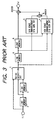
- FIG. 3 is a block diagram of a prior art video signal processing apparatus.
- This prior art video processing apparatus comprises a line memory 2 for delaying a video signal inputted to an input terminal Ti' by one horizontal line (scanning) period (1H), a line memory 3 for delaying an output of the line memory 2 by 1H, a noise reduction circuit 1, supplied with the video signal, the output of the line memory 2, and an output of the line memory 3, for reducing noises in the video signal through two-dimensional filtering, a line memory 8 for delaying an output of the noise reduction circuit 1 by 1H, a line memory 9 for delaying an output of the line memory 8 by 1H, a horizontal edge enhancement signal generation circuit 5 for generating a horizontal edge enhancement signal from an output of the line memory 8, a vertical edge enhancement signal generation circuit 4 for generating a vertical edge enhancement signal from outputs of the noise reduction circuit 1, the line memory 8, and the line memory 9, an adder 6 for summing the horizontal edge enhancement
- the noise reduction circuit 1 reducing noises in the video signal through two-dimensional filtering is disclosed in Japanese patent application provisional publication No. 6-86104.
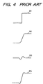
- Fig. 4 is a graphical drawing of the prior art video signal processing apparatus showing waveforms of output signals at respective points shown in Fig. 3.
- the line memory 2 delays the video signal, having a waveform 201, inputted through the input terminal Ti', by one horizontal scanning period (1H) to produce a one-H delayed video signal.
- the line memory 3 delays the output of the line memory 2 to produce two-H delayed video signal.
- the noise reduction circuit 1, supplied with the video signal, the one-H delayed video signal, and the two-H delayed video signal reduces noises in the video signal through two-dimensional filtering as shown by a waveform 202.
- the line memory 8 delays the output of the noise reduction circuit 1 by 1H.
- the line memory 9 delays the output of the line memory 8 by one horizontal scanning line.
- the horizontal edge enhancement signal generation circuit 5 generates the horizontal edge enhancement signal from the output of the line memory 8.
- the vertical edge enhancement signal generation circuit 4 generates the vertical edge enhancement signal from outputs of the noise reduction circuit 1, the line memory 8, the line memory 9.
- the adder 6 sums the horizontal edge enhancement signal and the vertical edge enhancement signal to produce an edge enhancement signal as shown be a waveform 203.
- the adder 7 sums the output of the line memory 9 and an output of the adder 6 to produce an edge enhanced video signal as shown by a waveform 204.
- the present invention has been developed in order to provide an improved video signal processing apparatus with noise reduction and edge enhancement.
- a first video signal processing apparatus for processing a video signal including a noise comprising: an edge enhancement signal generation circuit for generating an edge enhancement signal from the video signal; a noise reduction circuit for reducing a level of the noise to generate a noise reduced video signal; and an adder for adding the edge enhancement signal to the noise reduction video signal to output a processed video signal.
- This first video signal processing apparatus may further comprise an input terminal for receiving the video signal, wherein the edge enhancement signal generation circuit and the noise reduction circuit are coupled to the input terminal in parallel.
- This first video signal processing apparatus may further comprise a first delay circuit for delaying the video signal by one horizontal line period to generate a one-horizontal-line-period-delayed video signal and a second delay circuit responsive to the video signal for generating a two-horizontal-line-period-delayed video signal, wherein the edge enhancement signal generation circuit generates the edge enhanced signal from the video signal, the one-horizontal-line-period-delayed video signal, and the two-horizontal-line-period-delayed video signal and the noise reduction circuit generates the noise reduced video signal from the video signal, the one-horizontal-line-period-delayed video signal, and the two-horizontal-line-period-delayed video signal.
- the edge enhancement signal generation circuit may comprise a horizontal edge enhancement signal generation circuit responsive to the video signal for generating a horizontal edge enhancement signal, a vertical edge enhancement signal generation circuit responsive to the video signal for generating a vertical edge enhancement signal, and a second adder for adding the vertical edge enhancement signal to the horizontal edge enhancement signal to generate the edge enhancement signal.
- this apparatus may further comprise a first delay circuit for delaying the video signal by one horizontal line period to generate a one-horizontal-line-period-delayed video signal and a second delay circuit responsive to the video signal for generating a two-horizontal-line-period-delayed video signal, wherein the horizontal edge enhancement signal generation circuit generates the horizontal edge enhancement signal from the one-horizontal-period-delayed video signal and the vertical edge enhancement signal generation circuit generates the vertical edge enhancement signal from the video signal, the one-horizontal-period-delayed video signal, and the two-horizontal-period-delayed video signal.
- a second video signal processing apparatus for processing a video signal including a noise comprising: a first line memory for delaying a video signal by one horizontal line period to generate a one-horizontal-line-period-delayed video signal; a second line memory responsive to the video signal for generating a two-horizontal-line-period delayed video signal; a noise reduction circuit responsive to the video signal, the one-horizontal-line-period-delayed signal, and the two-horizontal-line-period-delayed signal for reducing a level of the noise to generate a noise reduced video signal through two-dimensional filtering; a horizontal edge enhancement signal generation circuit responsive to the one-horizontal-line-delayed signal for generating a horizontal edge enhancement signal; a vertical edge enhancement signal generation circuit responsive to the video signal, the one-horizontal-line-delayed signal, and the two-horizontal-line-delayed signal for generating a vertical edge enhancement signal; a first adder for adding the
- Fig. 1 is a block diagram of a video signal processing circuit of this invention.
- Fig. 2 is a graphical drawing of the video signal processing circuit showing waveforms at respective points of the video signal processing circuit shown in Fig. 1.
- the video signal processing circuit of this invention comprises a line memory 12 for delaying a video signal, having a waveform 101, inputted through an input terminal Ti, by one-horizontal line (1-H) to produce one-H delayed video signal, a line memory 13 for delaying the one-H delayed video signal from the line memory 12 by one-H to produce two-H delayed video signal, a noise reduction circuit 11, supplied with the video signal, the one-H delayed signal, and the two-H dealed signal, for reducing levels of noise included in the video signal to produce a noise reduced video signal as shown by waveform 102 through two-dimensional filtering, a horizontal edge enhancement signal generation circuit 15, supplied with the one-H delayed signal, for generating a horizontal edge enhancement signal as shown by a waveform 103, a vertical edge enhancement signal generation
- the line memory 12 delays the video signal, having a waveform 101, inputted through an input terminal Ti by one-H to produce one-H delayed video signal.
- the line memory 13 delays the one-H delayed video signal from the line memory 12 by one-H to produce two-H delayed video signal.
- the noise reduction device as disclosed in Japanese patent application provisional publication No 6-86104 can be used for this noise reduction circuit 11.
- the horizontal edge enhancement signal generation circuit 15, supplied with the one-H delayed signal comprises a delay circuit (not shown) for delaying the one-H delayed signal by one or more pixel periods to produce a delay signal as shown by a waveform 105 and detects and generates the horizontal edge enhancement signal through a differential operation between one-H delayed signal and the delay signal as shown by the waveform 105.
- the adder 16 adds the vertical edge enhancement signal to the horizontal edge enhancement signal to produce the edge enhancement signal.
- the adder 17 adds the edge enhancement signal to the video signal to produce the edge enhanced video signal, as shown by a waveform 104 and output the edge enhanced video signal at a terminal To.
- the noise reduction circuit 11 suppresses the noise included in the video signal irrespective of operations of the horizontal edge enhancement signal generation circuit 15 and the vertical edge enhancement signal generation circuit 14, so that a degree of the noise reduction can be determined irrespective of the operations of the horizontal edge enhancement signal generation circuit 15 and the vertical edge enhancement signal generation circuit 14.
- the horizontal edge enhancement signal generation circuit 15 and the vertical edge enhancement signal generation circuit 14 generates the horizontal edge enhancement signal and the vertical edge enhancement signal respectively irrespective of the operation of the noise reduction circuit 11, so that the horizontal and vertical edge enhancement signals can generate sharp horizontal and vertical edge enhancement signals respectively.
- the delayed video signals from the line memories 12 and 13 are commonly used for the noise reduction circuit 11 and for the edge enhancement circuit including the horizontal edge enhancement signal generation circuit 15 and the vertical edge enhancement signal generation circuit 14.
Landscapes
- Engineering & Computer Science (AREA)
- Multimedia (AREA)
- Signal Processing (AREA)
- Picture Signal Circuits (AREA)
Applications Claiming Priority (3)
| Application Number | Priority Date | Filing Date | Title |
|---|---|---|---|
| JP102273/95 | 1995-04-26 | ||
| JP10227395 | 1995-04-26 | ||
| JP7102273A JPH08298603A (ja) | 1995-04-26 | 1995-04-26 | 映像信号処理装置 |
Publications (3)
| Publication Number | Publication Date |
|---|---|
| EP0740465A2 true EP0740465A2 (fr) | 1996-10-30 |
| EP0740465A3 EP0740465A3 (fr) | 1998-09-23 |
| EP0740465B1 EP0740465B1 (fr) | 2001-06-20 |
Family
ID=14323002
Family Applications (1)
| Application Number | Title | Priority Date | Filing Date |
|---|---|---|---|
| EP96302939A Expired - Lifetime EP0740465B1 (fr) | 1995-04-26 | 1996-04-26 | Dispositif de traitement de signal vidéo avec réduction du bruit et amélioration des bords |
Country Status (4)
| Country | Link |
|---|---|
| US (1) | US5926577A (fr) |
| EP (1) | EP0740465B1 (fr) |
| JP (1) | JPH08298603A (fr) |
| DE (1) | DE69613428T2 (fr) |
Cited By (1)
| Publication number | Priority date | Publication date | Assignee | Title |
|---|---|---|---|---|
| US6867817B2 (en) | 2001-12-17 | 2005-03-15 | Koninklijke Philips Electronics N.V. | Natural luminance transient enhancement |
Families Citing this family (18)
| Publication number | Priority date | Publication date | Assignee | Title |
|---|---|---|---|---|
| DE19722358A1 (de) * | 1997-05-28 | 1998-12-03 | Thomson Brandt Gmbh | Verfahren zur Bearbeitung von Übergangsbereichen in einem Bildsignal |
| US6445831B1 (en) * | 1998-02-10 | 2002-09-03 | Fuji Photo Film Co., Ltd. | Image processing method and apparatus |
| JPH11250246A (ja) * | 1998-02-27 | 1999-09-17 | Fuji Photo Film Co Ltd | 画像処理方法および装置 |
| KR100296596B1 (ko) * | 1999-07-14 | 2001-07-12 | 윤종용 | 4방향 일차원 고역 통과 필터링에 의한 윤곽선 강조 방법 |
| JP2002057913A (ja) * | 2000-08-01 | 2002-02-22 | Nexpress Solutions Llc | 個人的好みに応じたカラー強調をもたらす像記録装置および像記録方法 |
| US7079287B1 (en) * | 2000-08-01 | 2006-07-18 | Eastman Kodak Company | Edge enhancement of gray level images |
| US7218420B1 (en) | 2000-08-01 | 2007-05-15 | Eastman Kodak Company | Gray level halftone processing |
| US7079281B1 (en) | 2000-08-01 | 2006-07-18 | Eastman Kodak Company | Edge enhancement processor and method with adjustable threshold setting |
| DE10114813C1 (de) * | 2001-03-26 | 2002-10-31 | Micronas Munich Gmbh | Verfahren und Vorrichtung zur Versteilerung von Signalübergängen bei Fernsehbildern |
| JP3933501B2 (ja) * | 2002-03-15 | 2007-06-20 | 富士フイルム株式会社 | ノイズ低減装置 |
| US7388621B2 (en) * | 2004-11-30 | 2008-06-17 | Mediatek Inc. | Systems and methods for image processing providing noise reduction and edge enhancement |
| US8018532B2 (en) * | 2006-02-02 | 2011-09-13 | Victor Company Of Japan, Ltd. | Video signal processing apparatus and method, and edge enhancement apparatus and method |
| JP4801626B2 (ja) * | 2007-05-18 | 2011-10-26 | Hoya株式会社 | 輪郭強調装置 |
| US8902319B2 (en) * | 2008-08-22 | 2014-12-02 | Sharp Kabushiki Kaisha | Image signal processing apparatus, image signal processing method, image display apparatus, television receiver, and electronic device |
| US8559746B2 (en) * | 2008-09-04 | 2013-10-15 | Silicon Image, Inc. | System, method, and apparatus for smoothing of edges in images to remove irregularities |
| JP4762336B2 (ja) * | 2009-09-15 | 2011-08-31 | 株式会社東芝 | 映像処理装置及び映像処理方法 |
| TWI456982B (zh) * | 2010-03-30 | 2014-10-11 | Realtek Semiconductor Corp | 影像處理裝置與空間影像雜訊消除方法 |
| JP2014135528A (ja) * | 2011-04-27 | 2014-07-24 | Sharp Corp | 画像処理装置、表示装置、画像処理方法および画像処理プログラム |
Family Cites Families (9)
| Publication number | Priority date | Publication date | Assignee | Title |
|---|---|---|---|---|
| JPH01220975A (ja) * | 1988-02-29 | 1989-09-04 | Toshiba Corp | 画質調整回路 |
| US5111511A (en) * | 1988-06-24 | 1992-05-05 | Matsushita Electric Industrial Co., Ltd. | Image motion vector detecting apparatus |
| US5130820A (en) * | 1989-02-25 | 1992-07-14 | Minolta Camera Kabushiki Kaisha | Image processing device |
| JPH02301295A (ja) * | 1989-05-15 | 1990-12-13 | Dainippon Printing Co Ltd | ビデオプリンタ装置 |
| GB2234133B (en) * | 1989-07-14 | 1993-11-10 | Mitsubishi Electric Corp | Video signal processing apparatus |
| US5542008A (en) * | 1990-02-28 | 1996-07-30 | Victor Company Of Japan, Ltd. | Method of and apparatus for compressing image representing signals |
| JPH0686104A (ja) * | 1992-09-04 | 1994-03-25 | Matsushita Electric Ind Co Ltd | ノイズリダクション装置 |
| JPH0766977A (ja) * | 1993-08-24 | 1995-03-10 | Minolta Co Ltd | 画像処理装置 |
| DE69421377T2 (de) * | 1994-02-28 | 2000-03-23 | Stmicroelectronics S.R.L., Agrate Brianza | Filter zur Rauschunterdrückung und Kantenverstärkung von numerischen Bildsignalen mit Hilfe unscharfer Logik |
-
1995
- 1995-04-26 JP JP7102273A patent/JPH08298603A/ja active Pending
-
1996
- 1996-04-25 US US08/637,490 patent/US5926577A/en not_active Expired - Lifetime
- 1996-04-26 DE DE69613428T patent/DE69613428T2/de not_active Expired - Lifetime
- 1996-04-26 EP EP96302939A patent/EP0740465B1/fr not_active Expired - Lifetime
Cited By (1)
| Publication number | Priority date | Publication date | Assignee | Title |
|---|---|---|---|---|
| US6867817B2 (en) | 2001-12-17 | 2005-03-15 | Koninklijke Philips Electronics N.V. | Natural luminance transient enhancement |
Also Published As
| Publication number | Publication date |
|---|---|
| JPH08298603A (ja) | 1996-11-12 |
| DE69613428D1 (de) | 2001-07-26 |
| DE69613428T2 (de) | 2001-11-08 |
| EP0740465B1 (fr) | 2001-06-20 |
| US5926577A (en) | 1999-07-20 |
| EP0740465A3 (fr) | 1998-09-23 |
Similar Documents
| Publication | Publication Date | Title |
|---|---|---|
| US5926577A (en) | Video signal processing apparatus with noise reduction and edge enhancement | |
| JPH0763133B2 (ja) | スケール係数発生回路 | |
| KR970057474A (ko) | 비디오 신호의 로컬 콘트라스트 개선을 위한 방법 및 장치 | |
| US4924315A (en) | Video signal processing system | |
| US6278494B1 (en) | Edge emphasis device, image forming apparatus using the same, image signal processing method, and image forming method using the same | |
| JPH04326689A (ja) | 補間及び走査線変換回路 | |
| US5404179A (en) | Noise reduction apparatus for video image | |
| EP2669864B1 (fr) | Dispositif de traitement de signal vidéo et procédé | |
| US5218438A (en) | Picture aperture correction circuit | |
| JP4247220B2 (ja) | 動き適応順次走査変換装置及び変換方法 | |
| KR20030011537A (ko) | 화상 신호 처리 장치 | |
| EP1411633A3 (fr) | Traitement de signaux faibles basé à l'élimination de bruit d'impulsions | |
| US5543859A (en) | Horizontal contour emphasizing signal processor | |
| US5748258A (en) | Apparatus and method for processing a video signal | |
| JP3111850B2 (ja) | ノイズ除去回路及びmuseデコーダ | |
| JP2000244775A (ja) | 輪郭強調装置 | |
| JP2871323B2 (ja) | 映像信号処理装置 | |
| JP3233331B2 (ja) | 輪郭補正回路 | |
| JPH114363A (ja) | 輪郭補正回路 | |
| JP2565178B2 (ja) | 非線形フィルタ | |
| JP2536500B2 (ja) | 輪郭補正回路 | |
| JP2000341557A (ja) | 輪郭補正回路 | |
| JPH08102889A (ja) | 画像特殊効果装置 | |
| JP2570272B2 (ja) | デジタル輪郭強調回路 | |
| JP3314579B2 (ja) | 水平輪郭強調信号処理回路 |
Legal Events
| Date | Code | Title | Description |
|---|---|---|---|
| PUAI | Public reference made under article 153(3) epc to a published international application that has entered the european phase |
Free format text: ORIGINAL CODE: 0009012 |
|
| 17P | Request for examination filed |
Effective date: 19960503 |
|
| AK | Designated contracting states |
Kind code of ref document: A2 Designated state(s): DE FR GB |
|
| PUAL | Search report despatched |
Free format text: ORIGINAL CODE: 0009013 |
|
| AK | Designated contracting states |
Kind code of ref document: A3 Designated state(s): DE FR GB |
|
| 17Q | First examination report despatched |
Effective date: 19990208 |
|
| GRAG | Despatch of communication of intention to grant |
Free format text: ORIGINAL CODE: EPIDOS AGRA |
|
| GRAG | Despatch of communication of intention to grant |
Free format text: ORIGINAL CODE: EPIDOS AGRA |
|
| GRAH | Despatch of communication of intention to grant a patent |
Free format text: ORIGINAL CODE: EPIDOS IGRA |
|
| GRAH | Despatch of communication of intention to grant a patent |
Free format text: ORIGINAL CODE: EPIDOS IGRA |
|
| GRAA | (expected) grant |
Free format text: ORIGINAL CODE: 0009210 |
|
| AK | Designated contracting states |
Kind code of ref document: B1 Designated state(s): DE FR GB |
|
| REF | Corresponds to: |
Ref document number: 69613428 Country of ref document: DE Date of ref document: 20010726 |
|
| ET | Fr: translation filed | ||
| REG | Reference to a national code |
Ref country code: GB Ref legal event code: IF02 |
|
| PLBE | No opposition filed within time limit |
Free format text: ORIGINAL CODE: 0009261 |
|
| STAA | Information on the status of an ep patent application or granted ep patent |
Free format text: STATUS: NO OPPOSITION FILED WITHIN TIME LIMIT |
|
| 26N | No opposition filed | ||
| PGFP | Annual fee paid to national office [announced via postgrant information from national office to epo] |
Ref country code: FR Payment date: 20090417 Year of fee payment: 14 |
|
| PGFP | Annual fee paid to national office [announced via postgrant information from national office to epo] |
Ref country code: GB Payment date: 20100325 Year of fee payment: 15 |
|
| PGFP | Annual fee paid to national office [announced via postgrant information from national office to epo] |
Ref country code: DE Payment date: 20100430 Year of fee payment: 15 |
|
| REG | Reference to a national code |
Ref country code: FR Ref legal event code: ST Effective date: 20101230 |
|
| REG | Reference to a national code |
Ref country code: DE Ref legal event code: R119 Ref document number: 69613428 Country of ref document: DE |
|
| REG | Reference to a national code |
Ref country code: DE Ref legal event code: R119 Ref document number: 69613428 Country of ref document: DE |
|
| GBPC | Gb: european patent ceased through non-payment of renewal fee |
Effective date: 20110426 |
|
| PG25 | Lapsed in a contracting state [announced via postgrant information from national office to epo] |
Ref country code: GB Free format text: LAPSE BECAUSE OF NON-PAYMENT OF DUE FEES Effective date: 20110426 |
|
| PG25 | Lapsed in a contracting state [announced via postgrant information from national office to epo] |
Ref country code: FR Free format text: LAPSE BECAUSE OF NON-PAYMENT OF DUE FEES Effective date: 20100430 |
|
| PG25 | Lapsed in a contracting state [announced via postgrant information from national office to epo] |
Ref country code: DE Free format text: LAPSE BECAUSE OF NON-PAYMENT OF DUE FEES Effective date: 20111031 |