EP0741432A2 - Verfahren und Vorrichtung für HTS-Übertragungsleitungen mit hoher Leistung unter Verwendung durch eine Spalte getrennter Streifen - Google Patents
Verfahren und Vorrichtung für HTS-Übertragungsleitungen mit hoher Leistung unter Verwendung durch eine Spalte getrennter Streifen Download PDFInfo
- Publication number
- EP0741432A2 EP0741432A2 EP96303075A EP96303075A EP0741432A2 EP 0741432 A2 EP0741432 A2 EP 0741432A2 EP 96303075 A EP96303075 A EP 96303075A EP 96303075 A EP96303075 A EP 96303075A EP 0741432 A2 EP0741432 A2 EP 0741432A2
- Authority
- EP
- European Patent Office
- Prior art keywords
- strips
- transmission line
- gap
- microstrip
- substrate
- Prior art date
- Legal status (The legal status is an assumption and is not a legal conclusion. Google has not performed a legal analysis and makes no representation as to the accuracy of the status listed.)
- Withdrawn
Links
- 230000005540 biological transmission Effects 0.000 title claims abstract description 59
- 238000000034 method Methods 0.000 title claims description 8
- 239000000758 substrate Substances 0.000 claims abstract description 18
- 239000000463 material Substances 0.000 claims abstract description 6
- 239000003989 dielectric material Substances 0.000 claims description 2
- 230000008878 coupling Effects 0.000 description 5
- 238000010168 coupling process Methods 0.000 description 5
- 238000005859 coupling reaction Methods 0.000 description 5
- 238000004088 simulation Methods 0.000 description 2
- RYGMFSIKBFXOCR-UHFFFAOYSA-N Copper Chemical compound [Cu] RYGMFSIKBFXOCR-UHFFFAOYSA-N 0.000 description 1
- BQCADISMDOOEFD-UHFFFAOYSA-N Silver Chemical compound [Ag] BQCADISMDOOEFD-UHFFFAOYSA-N 0.000 description 1
- 239000003990 capacitor Substances 0.000 description 1
- 238000004891 communication Methods 0.000 description 1
- 239000012141 concentrate Substances 0.000 description 1
- 239000004020 conductor Substances 0.000 description 1
- 238000010276 construction Methods 0.000 description 1
- 229910052802 copper Inorganic materials 0.000 description 1
- 239000010949 copper Substances 0.000 description 1
- 230000000694 effects Effects 0.000 description 1
- 238000005516 engineering process Methods 0.000 description 1
- -1 for example Substances 0.000 description 1
- PCHJSUWPFVWCPO-UHFFFAOYSA-N gold Chemical compound [Au] PCHJSUWPFVWCPO-UHFFFAOYSA-N 0.000 description 1
- 229910052737 gold Inorganic materials 0.000 description 1
- 239000010931 gold Substances 0.000 description 1
- 238000003780 insertion Methods 0.000 description 1
- 230000037431 insertion Effects 0.000 description 1
- 229910052709 silver Inorganic materials 0.000 description 1
- 239000004332 silver Substances 0.000 description 1
- 239000007787 solid Substances 0.000 description 1
Images





Classifications
-
- H—ELECTRICITY
- H01—ELECTRIC ELEMENTS
- H01P—WAVEGUIDES; RESONATORS, LINES, OR OTHER DEVICES OF THE WAVEGUIDE TYPE
- H01P3/00—Waveguides; Transmission lines of the waveguide type
- H01P3/02—Waveguides; Transmission lines of the waveguide type with two longitudinal conductors
- H01P3/08—Microstrips; Strip lines
- H01P3/085—Triplate lines
-
- H—ELECTRICITY
- H01—ELECTRIC ELEMENTS
- H01P—WAVEGUIDES; RESONATORS, LINES, OR OTHER DEVICES OF THE WAVEGUIDE TYPE
- H01P3/00—Waveguides; Transmission lines of the waveguide type
- H01P3/02—Waveguides; Transmission lines of the waveguide type with two longitudinal conductors
- H01P3/08—Microstrips; Strip lines
- H01P3/081—Microstriplines
-
- H—ELECTRICITY
- H01—ELECTRIC ELEMENTS
- H01P—WAVEGUIDES; RESONATORS, LINES, OR OTHER DEVICES OF THE WAVEGUIDE TYPE
- H01P7/00—Resonators of the waveguide type
- H01P7/08—Strip line resonators
- H01P7/082—Microstripline resonators
-
- H—ELECTRICITY
- H01—ELECTRIC ELEMENTS
- H01P—WAVEGUIDES; RESONATORS, LINES, OR OTHER DEVICES OF THE WAVEGUIDE TYPE
- H01P7/00—Resonators of the waveguide type
- H01P7/08—Strip line resonators
- H01P7/084—Triplate line resonators
-
- Y—GENERAL TAGGING OF NEW TECHNOLOGICAL DEVELOPMENTS; GENERAL TAGGING OF CROSS-SECTIONAL TECHNOLOGIES SPANNING OVER SEVERAL SECTIONS OF THE IPC; TECHNICAL SUBJECTS COVERED BY FORMER USPC CROSS-REFERENCE ART COLLECTIONS [XRACs] AND DIGESTS
- Y10—TECHNICAL SUBJECTS COVERED BY FORMER USPC
- Y10S—TECHNICAL SUBJECTS COVERED BY FORMER USPC CROSS-REFERENCE ART COLLECTIONS [XRACs] AND DIGESTS
- Y10S428/00—Stock material or miscellaneous articles
- Y10S428/922—Static electricity metal bleed-off metallic stock
- Y10S428/9265—Special properties
- Y10S428/93—Electric superconducting
-
- Y—GENERAL TAGGING OF NEW TECHNOLOGICAL DEVELOPMENTS; GENERAL TAGGING OF CROSS-SECTIONAL TECHNOLOGIES SPANNING OVER SEVERAL SECTIONS OF THE IPC; TECHNICAL SUBJECTS COVERED BY FORMER USPC CROSS-REFERENCE ART COLLECTIONS [XRACs] AND DIGESTS
- Y10—TECHNICAL SUBJECTS COVERED BY FORMER USPC
- Y10S—TECHNICAL SUBJECTS COVERED BY FORMER USPC CROSS-REFERENCE ART COLLECTIONS [XRACs] AND DIGESTS
- Y10S505/00—Superconductor technology: apparatus, material, process
- Y10S505/70—High TC, above 30 k, superconducting device, article, or structured stock
- Y10S505/701—Coated or thin film device, i.e. active or passive
-
- Y—GENERAL TAGGING OF NEW TECHNOLOGICAL DEVELOPMENTS; GENERAL TAGGING OF CROSS-SECTIONAL TECHNOLOGIES SPANNING OVER SEVERAL SECTIONS OF THE IPC; TECHNICAL SUBJECTS COVERED BY FORMER USPC CROSS-REFERENCE ART COLLECTIONS [XRACs] AND DIGESTS
- Y10—TECHNICAL SUBJECTS COVERED BY FORMER USPC
- Y10S—TECHNICAL SUBJECTS COVERED BY FORMER USPC CROSS-REFERENCE ART COLLECTIONS [XRACs] AND DIGESTS
- Y10S505/00—Superconductor technology: apparatus, material, process
- Y10S505/70—High TC, above 30 k, superconducting device, article, or structured stock
- Y10S505/701—Coated or thin film device, i.e. active or passive
- Y10S505/703—Microelectronic device with superconducting conduction line
-
- Y—GENERAL TAGGING OF NEW TECHNOLOGICAL DEVELOPMENTS; GENERAL TAGGING OF CROSS-SECTIONAL TECHNOLOGIES SPANNING OVER SEVERAL SECTIONS OF THE IPC; TECHNICAL SUBJECTS COVERED BY FORMER USPC CROSS-REFERENCE ART COLLECTIONS [XRACs] AND DIGESTS
- Y10—TECHNICAL SUBJECTS COVERED BY FORMER USPC
- Y10S—TECHNICAL SUBJECTS COVERED BY FORMER USPC CROSS-REFERENCE ART COLLECTIONS [XRACs] AND DIGESTS
- Y10S505/00—Superconductor technology: apparatus, material, process
- Y10S505/825—Apparatus per se, device per se, or process of making or operating same
- Y10S505/866—Wave transmission line, network, waveguide, or microwave storage device
-
- Y—GENERAL TAGGING OF NEW TECHNOLOGICAL DEVELOPMENTS; GENERAL TAGGING OF CROSS-SECTIONAL TECHNOLOGIES SPANNING OVER SEVERAL SECTIONS OF THE IPC; TECHNICAL SUBJECTS COVERED BY FORMER USPC CROSS-REFERENCE ART COLLECTIONS [XRACs] AND DIGESTS
- Y10—TECHNICAL SUBJECTS COVERED BY FORMER USPC
- Y10T—TECHNICAL SUBJECTS COVERED BY FORMER US CLASSIFICATION
- Y10T428/00—Stock material or miscellaneous articles
- Y10T428/24—Structurally defined web or sheet [e.g., overall dimension, etc.]
- Y10T428/24802—Discontinuous or differential coating, impregnation or bond [e.g., artwork, printing, retouched photograph, etc.]
- Y10T428/24926—Discontinuous or differential coating, impregnation or bond [e.g., artwork, printing, retouched photograph, etc.] including ceramic, glass, porcelain or quartz layer
Definitions
- This invention relates to microstrip/stripline transmission lines and microstrip/stripline filters and to a method of construction thereof. More particularly, this invention relates to filters and transmission lines having at least a portion thereof divided into elongated strips.
- Microstrip or stripline filters are an important part of microwave circuit designs. Generally, these filters are used in low Q and low power applications because firstly, the conventional conducting materials, for example, gold, silver, copper, etc. are relatively lossy and, secondly, the cross-section current distribution of a microstrip/stripline filter is highly non-uniform. High Q can be achieved for narrow band microstrip/stripline filters when they are constructed of high temperature superconductive (HTS) materials. HTS materials improve the power handling capability of these filters as they have a low loss and high current capacity. It is known to provide filters with improved power handling capability by using low impedance lines and dual-mode patch resonators. Microwave filters using dual-mode patch resonator structures can handle more power than single mode line resonator filters because of the patch size. However, there are limitations on the layout and therefore the size of the filter.
- HTS high temperature superconductive
- microstrip transmission lines, resonators and filters are considered to be equivalent to stripline transmission lines, resonators and filters. Any transmission line, resonator or filter that can be made of microstrip can also be made of stripline.
- the transmission line can be a resonator and can be included in any microwave circuit including a filter.
- a microwave transmission line for carrying current at microwave frequencies comprises several elongated strips selected from the group consisting of microstrip and stripline. Each strip has an input end and an output end. The strips are arranged on a substrate with a gap between at least two adjacent strips. Preferably, there is a gap between each of the adjacent strips.
- a prior art microstrip transmission line 2 has an elongated piece 4 of microstrip arranged on a substrate 6 of dielectric material.
- the substrate 6 has a top 8 and a bottom 10 with a conducting layer 12 covering the bottom 10 as a ground plane.
- Figure 2 is an end view of the prior art microstrip transmission line of Figure 1 and Figure 3 is a graph that schematically illustrates a current density 14 across the width of the microstrip line 4. It can be seen from Figure 3 that the current density near the outside edges of the microstrip 4 is considerably higher than the current density elsewhere on the microstrip. Stripline structure can readily be substituted for the microstrip structure in Figures 1 and 2.
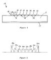
- FIG 4 there is shown an end view of a microstrip transmission line 16 for carrying current at microwave frequencies.
- the transmission line 16 has several elongated strips 18, 20, 22, 24, 26, 28, 30, 32 with a gap 34 located between adjacent strips. Each strip has a width W and each gap has a size S.
- the strips are arranged on a substrate 6 with a ground plane 12, these components being identical to those of the prior art transmission line 2.
- the strips 18, 20, 22, 24, 26, 28, 30, 32 have a rectangular shape with side edges that are parallel to one another.
- Each strip has the same size W and the gaps 34 between the strips have an identical size S.
- the width W and/or the gap size S of each of the strips could vary across the transmission line. The number of strips could also vary from that shown in Figure 4.
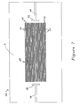
- the current distributes between the strips as schematically shown in the graph of Figure 5 where the current density 18a, 20a, 22a, 24a, 26a, 28a, 30a, 32a corresponds to the current density of the strips 18, 20, 22, 24, 26, 28, 30, 32 respectively.
- the current density along the outer edges of the two outer strips 18, 32 is much higher than the current density on the remaining strips but is much less than the maximum current density shown for the prior art transmission line in Figure 3.
- the current density of the strips 24, 26 at centre of the transmission line is higher at the outer edges thereof than in the remainder of said strips 24, 26.
- the current density on the strips 18, 20, 22, 28, 30, 32 is highest on an outer edge of said strips 18, 20, 22, 28, 30, 32. Still further, it can be seen that the current density is distributed more evenly in Figure 5 than the current density for the prior art transmission line shown in Figure 3.
- the number of strips for a particular transmission line is determined by the selection of the width of each strip and the gap size between adjacent strips.
- the cross-section current distribution can be fine tuned with proper selection of W and S for the strips and gap size across the line.
- FIG 6 there is shown a schematic top view of a prior art single half wavelength microstrip resonator circuit 35 on a substrate 6.
- the circuit has a ground plane beneath the substrate 6 (as in Figure 1), which is not shown in Figure 6.
- the circuit 35 has an input line 36, a coupling line 38, a solid microstrip resonator 40, a coupling line 42 and an output line 44.
- a microstrip resonator circuit 46 is shown.
- the same reference numerals are used in Figure 7 for those components that are virtually identical to those of Figure 6.
- the circuits 46 and 35 are identical except for the resonator.
- the circuit 46 has a resonator 48 that is made up of several elongated strips 50.
- the strips 50 are rectangular in shape with parallel side edges and a gap 34 between adjacent strips.
- the circuit 46 also has a ground plane (not shown).
- FIG 8 a graph of the current density distribution across one-half of a cross-section through a center of the resonator 40 is shown.
- Em software Em User's Manual, Sonnet Software Inc., 135 Old Cove Road, Suite 203, Liverpool, New York, 13090-3774
- a maximum current density of 1262 A/m is indicated for an outside edge of the resonator 40.
- the current density distribution is only shown for half of the resonator, the current density distribution of the other half of the resonator would be virtually identical to the half that is shown with the current density along the two outer edges being the maximum current density.
- the simulation was done assuming that the line thickness is infinitely thin and the cell size (i.e. the resolution) is 1.0 mil by 0.5 mil, with a resonator size of 234 mil by 84 mil.
- FIG 10 there is shown a top view of a three-pole microstrip pseudo-lumped element filter 52 for high power applications.
- the filter has an input line 36 and a coupling line 38.
- the filter 52 has an output coupling line 42 and an output line 44.
- Between the coupling lines 38, 42 are three lumped elements 54 which are spaced apart from one another.
- Each lumped element 54 has a central section 56 that emulates inductors and two end sections 58 that emulate capacitors.
- the center sections 56 are divided into several strips 50 separated by gaps 34.
- the filter 52 was constructed using high temperature superconductive material.
- Figure 11 is a graph showing the measured electrical responses, being the insertion loss and return loss at 77K.
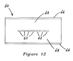
- stripline transmission line 60 there is shown a stripline transmission line 60.
- the stripline 60 has a plurality of strips 62 sandwiched between two substrates 64 and two ground planes 66. It is well known that stripline is equivalent to microstrip and that stripline has two substrates and two ground planes in a "sandwich" arrangement and microstrip has only one ground plane.
- FIG 13 there is shown a schematic top view of strips 68, 70, 72 of a microstrip/stripline transmission line (not shown).
- the strips 68 have an identical width and are narrower than the strips 70.
- the strips 70 have an identical width and are narrower than the single strip 72.
- Gaps 74 between strips 68, 70 are identical to one another and are narrower than gaps 76 located between strips 70, 72.
- FIG 14 there is shown a schematic top view of strips 78, 80, 82 of a microstrip/stripline transmission line (not shown).
- the strips 78, 80, 82 curve smoothly through a 90° curve.
- Strips 78 are identical to one another and are narrower than strips 80, which in turn are narrower than the center strip 82.
- gaps 84 between strips 78, 80 are narrower than gaps 86 between strips 80, 82.
- the microstrip/stripline transmission line of the present invention can be used in any microstrip/stripline circuit either for connecting, or as a resonator, or part of a resonator to improve the power handling capability of that particular transmission line.
- the invention can be used in a filter using multiples of quarter wavelength transmission line as resonators, in a stepped impedance filter, a lumped element filter where the inductors are approximated by a piece of transmission line, in comb-line and in hairpin-line filters.
- the strips are curved.
- the strips could be S-shaped and the edges of the strips could be parallel or non-parallel.
- the width of the strips can vary in size as can the gap size across different strips.
Landscapes
- Control Of Motors That Do Not Use Commutators (AREA)
Applications Claiming Priority (2)
| Application Number | Priority Date | Filing Date | Title |
|---|---|---|---|
| CA2148341 | 1995-05-01 | ||
| CA002148341A CA2148341C (en) | 1995-05-01 | 1995-05-01 | Method and structure for high power hts transmission lines using strips separated by a gap |
Publications (2)
| Publication Number | Publication Date |
|---|---|
| EP0741432A2 true EP0741432A2 (de) | 1996-11-06 |
| EP0741432A3 EP0741432A3 (de) | 1998-03-04 |
Family
ID=4155769
Family Applications (1)
| Application Number | Title | Priority Date | Filing Date |
|---|---|---|---|
| EP96303075A Withdrawn EP0741432A3 (de) | 1995-05-01 | 1996-05-01 | Verfahren und Vorrichtung für HTS-Übertragungsleitungen mit hoher Leistung unter Verwendung durch eine Spalte getrennter Streifen |
Country Status (3)
| Country | Link |
|---|---|
| US (1) | US5922650A (de) |
| EP (1) | EP0741432A3 (de) |
| CA (1) | CA2148341C (de) |
Cited By (4)
| Publication number | Priority date | Publication date | Assignee | Title |
|---|---|---|---|---|
| US6144268A (en) * | 1997-10-09 | 2000-11-07 | Murata Manufacturing Co., Ltd. | High-frequency transmission line, dielectric resonator, filter, duplexer, and communication device, with an electrode having gaps in an edge portion |
| EP0984502A3 (de) * | 1998-09-01 | 2001-08-16 | Murata Manufacturing Co., Ltd. | Verlustarme Hochfrequenzelektrode |
| EP0984501A3 (de) * | 1998-09-01 | 2001-08-16 | Murata Manufacturing Co., Ltd. | Verlustarme Hochfrequenzelektrode |
| EP2065965A1 (de) * | 2007-11-26 | 2009-06-03 | Kabushiki Kaisha Toshiba | Resonator und Filter |
Families Citing this family (11)
| Publication number | Priority date | Publication date | Assignee | Title |
|---|---|---|---|---|
| US6792299B2 (en) | 2001-03-21 | 2004-09-14 | Conductus, Inc. | Device approximating a shunt capacitor for strip-line-type circuits |
| JP3861806B2 (ja) * | 2001-12-18 | 2006-12-27 | 株式会社村田製作所 | 共振器、フィルタ、デュプレクサ、および通信装置 |
| US7071797B2 (en) * | 2002-02-19 | 2006-07-04 | Conductus, Inc. | Method and apparatus for minimizing intermodulation with an asymmetric resonator |
| JP3660338B2 (ja) * | 2002-11-07 | 2005-06-15 | 株式会社東芝 | 伝送線路及び半導体装置 |
| US20050062137A1 (en) * | 2003-09-18 | 2005-03-24 | International Business Machines Corporation | Vertically-stacked co-planar transmission line structure for IC design |
| JP4992345B2 (ja) * | 2006-08-31 | 2012-08-08 | パナソニック株式会社 | 伝送線路型共振器と、これを用いた高周波フィルタ、高周波モジュールおよび無線機器 |
| EP2145393A1 (de) * | 2007-05-10 | 2010-01-20 | Superconductor Technologies, Inc. | Zickzack-array-resonatoren für hts-anwendungen mit relativ hoher leistung |
| US10903543B2 (en) | 2016-12-06 | 2021-01-26 | Hewlett Packard Enterprise Development Lp | PCB transmission lines having reduced loss |
| US10784553B2 (en) * | 2018-09-07 | 2020-09-22 | International Business Machines Corporation | Well thermalized stripline formation for high-density connections in quantum applications |
| US11805594B2 (en) * | 2020-08-04 | 2023-10-31 | Dell Products L.P. | Information handling system with split trace for high speed routing |
| DE102021115979A1 (de) * | 2021-06-21 | 2022-12-22 | HELLA GmbH & Co. KGaA | UWB-Bandpassfilter |
Family Cites Families (14)
| Publication number | Priority date | Publication date | Assignee | Title |
|---|---|---|---|---|
| GB747703A (en) * | 1953-12-22 | 1956-04-11 | Emi Ltd | Improvements in or relating to electrical transmission lines |
| US4441088A (en) * | 1981-12-31 | 1984-04-03 | International Business Machines Corporation | Stripline cable with reduced crosstalk |
| WO1983002687A1 (en) * | 1982-01-21 | 1983-08-04 | Communications Satellite Corp | Low impedance coplanar microwave transmission line |
| US4583064A (en) * | 1983-09-02 | 1986-04-15 | Matsushita Electric Industrial Co., Ltd. | Strip-line resonator |
| US4926189A (en) * | 1988-05-10 | 1990-05-15 | Communications Satellite Corporation | High-gain single- and dual-polarized antennas employing gridded printed-circuit elements |
| JPH03286601A (ja) * | 1990-04-03 | 1991-12-17 | Res Dev Corp Of Japan | マイクロ波共振器 |
| US5012319A (en) * | 1990-05-14 | 1991-04-30 | At&T Bell Laboratories | Integrated electronic assembly comprising a transmission line |
| US5406233A (en) * | 1991-02-08 | 1995-04-11 | Massachusetts Institute Of Technology | Tunable stripline devices |
| KR950003713B1 (ko) * | 1992-05-29 | 1995-04-17 | 삼성전자 주식회사 | 평행선로 대역통과여파기 |
| JP3241139B2 (ja) * | 1993-02-04 | 2001-12-25 | 三菱電機株式会社 | フィルムキャリア信号伝送線路 |
| JP3587264B2 (ja) * | 1993-09-22 | 2004-11-10 | 株式会社村田製作所 | ストリップ線路とそれを用いる伝送線路,共振器およびフィルタ |
| US5616538A (en) * | 1994-06-06 | 1997-04-01 | Superconductor Technologies, Inc. | High temperature superconductor staggered resonator array bandpass filter |
| US5496795A (en) * | 1994-08-16 | 1996-03-05 | Das; Satyendranath | High TC superconducting monolithic ferroelectric junable b and pass filter |
| US5703020A (en) * | 1995-05-30 | 1997-12-30 | Das; Satyendranath | High Tc superconducting ferroelectric MMIC phase shifters |
-
1995
- 1995-05-01 CA CA002148341A patent/CA2148341C/en not_active Expired - Fee Related
-
1996
- 1996-02-06 US US08/595,864 patent/US5922650A/en not_active Expired - Fee Related
- 1996-05-01 EP EP96303075A patent/EP0741432A3/de not_active Withdrawn
Cited By (8)
| Publication number | Priority date | Publication date | Assignee | Title |
|---|---|---|---|---|
| US6144268A (en) * | 1997-10-09 | 2000-11-07 | Murata Manufacturing Co., Ltd. | High-frequency transmission line, dielectric resonator, filter, duplexer, and communication device, with an electrode having gaps in an edge portion |
| EP0917236A3 (de) * | 1997-10-09 | 2001-03-14 | Murata Manufacturing Co., Ltd. | Hochfrequenzübertragungsleitung, dielektrischer Resonator, Filter, Duplexer und Kommunikationsgerät |
| EP0984502A3 (de) * | 1998-09-01 | 2001-08-16 | Murata Manufacturing Co., Ltd. | Verlustarme Hochfrequenzelektrode |
| EP0984501A3 (de) * | 1998-09-01 | 2001-08-16 | Murata Manufacturing Co., Ltd. | Verlustarme Hochfrequenzelektrode |
| US6438395B1 (en) | 1998-09-01 | 2002-08-20 | Murata Manufacturing Co., Ltd. | High frequency low loss electrode with main and sub conductors |
| US6456861B1 (en) | 1998-09-01 | 2002-09-24 | Murata Manufacturing Co., Ltd. | High frequency low loss electrode having laminated main and sub conductors |
| EP2065965A1 (de) * | 2007-11-26 | 2009-06-03 | Kabushiki Kaisha Toshiba | Resonator und Filter |
| US7983728B2 (en) | 2007-11-26 | 2011-07-19 | Kabushiki Kaisha Toshiba | Resonator comprised of a bent conductor line with slits therein and a filter formed therefrom |
Also Published As
| Publication number | Publication date |
|---|---|
| US5922650A (en) | 1999-07-13 |
| EP0741432A3 (de) | 1998-03-04 |
| CA2148341C (en) | 1997-02-04 |
| CA2148341A1 (en) | 1996-11-02 |
Similar Documents
| Publication | Publication Date | Title |
|---|---|---|
| CA2148341C (en) | Method and structure for high power hts transmission lines using strips separated by a gap | |
| US6370404B1 (en) | High temperature superconductor mini-filters and mini-multiplexers with self-resonant spiral resonators | |
| US5616538A (en) | High temperature superconductor staggered resonator array bandpass filter | |
| US6026311A (en) | High temperature superconducting structures and methods for high Q, reduced intermodulation resonators and filters | |
| CA2166014C (en) | High power superconductive circuits and method of construction thereof | |
| US6122533A (en) | Superconductive planar radio frequency filter having resonators with folded legs | |
| WO1998000880A9 (en) | Planar radio frequency filter | |
| JPH11177310A (ja) | 高周波伝送線路、誘電体共振器、フィルタ、デュプレクサおよび通信機 | |
| EP1148576A2 (de) | Filterschaltung und supraleitende Filterschaltung | |
| EP1265310B1 (de) | Supraleitendes mikrostreifenfilter | |
| US20020158704A1 (en) | Device approximating a shunt capacitor for strip-line-type circuits | |
| EP2145393A1 (de) | Zickzack-array-resonatoren für hts-anwendungen mit relativ hoher leistung | |
| US5801605A (en) | Distributed TEM filter with interdigital array of resonators | |
| US7231238B2 (en) | High temperature spiral snake superconducting resonator having wider runs with higher current density | |
| JP3391271B2 (ja) | 高周波用低損失電極 | |
| US7276989B2 (en) | Attenuator circuit comprising a plurality of quarter wave transformers and lump element resistors | |
| GB2153155A (en) | Improvements on or relating to microwave filters | |
| EP1564834B1 (de) | Mikrowellenfilter | |
| KR100303464B1 (ko) | 고주파 회로 소자 | |
| KR20100135272A (ko) | 초소형 모놀리식 전자기 공진기 | |
| KR100313893B1 (ko) | 협대역 초전도 대역 통과 필터 | |
| Cassinese et al. | Superconducting planar filters using dual-mode cross-slotted square resonators | |
| EP1820236B1 (de) | Übertragungsanordnung | |
| US20020005766A1 (en) | RF resonator | |
| US20080039333A1 (en) | High temperature superconducting structures and methods for high Q, reduced intermodulation structures |
Legal Events
| Date | Code | Title | Description |
|---|---|---|---|
| PUAI | Public reference made under article 153(3) epc to a published international application that has entered the european phase |
Free format text: ORIGINAL CODE: 0009012 |
|
| AK | Designated contracting states |
Kind code of ref document: A2 Designated state(s): DE FR GB IT |
|
| PUAL | Search report despatched |
Free format text: ORIGINAL CODE: 0009013 |
|
| AK | Designated contracting states |
Kind code of ref document: A3 Designated state(s): DE FR GB IT |
|
| 17P | Request for examination filed |
Effective date: 19980717 |
|
| 17Q | First examination report despatched |
Effective date: 20010704 |
|
| GRAP | Despatch of communication of intention to grant a patent |
Free format text: ORIGINAL CODE: EPIDOSNIGR1 |
|
| STAA | Information on the status of an ep patent application or granted ep patent |
Free format text: STATUS: THE APPLICATION IS DEEMED TO BE WITHDRAWN |
|
| 18D | Application deemed to be withdrawn |
Effective date: 20031202 |