EP0742619A2 - Oberflächenemittierender Laser mit verbessertem Wirkungsgrad - Google Patents
Oberflächenemittierender Laser mit verbessertem Wirkungsgrad Download PDFInfo
- Publication number
- EP0742619A2 EP0742619A2 EP96302076A EP96302076A EP0742619A2 EP 0742619 A2 EP0742619 A2 EP 0742619A2 EP 96302076 A EP96302076 A EP 96302076A EP 96302076 A EP96302076 A EP 96302076A EP 0742619 A2 EP0742619 A2 EP 0742619A2
- Authority
- EP
- European Patent Office
- Prior art keywords
- laser
- mirror
- bandwidths
- gain medium
- active
- Prior art date
- Legal status (The legal status is an assumption and is not a legal conclusion. Google has not performed a legal analysis and makes no representation as to the accuracy of the status listed.)
- Granted
Links
- 238000005086 pumping Methods 0.000 title claims abstract description 11
- 230000003287 optical effect Effects 0.000 claims abstract description 18
- 239000000758 substrate Substances 0.000 claims abstract description 14
- 230000004888 barrier function Effects 0.000 claims abstract description 11
- 239000000463 material Substances 0.000 claims description 10
- 229910001218 Gallium arsenide Inorganic materials 0.000 claims description 4
- 239000004065 semiconductor Substances 0.000 claims description 2
- 238000002310 reflectometry Methods 0.000 description 25
- 230000005855 radiation Effects 0.000 description 6
- 239000011149 active material Substances 0.000 description 4
- 239000000203 mixture Substances 0.000 description 4
- 230000007423 decrease Effects 0.000 description 3
- 230000005540 biological transmission Effects 0.000 description 2
- 229910000980 Aluminium gallium arsenide Inorganic materials 0.000 description 1
- 238000003491 array Methods 0.000 description 1
- 239000000969 carrier Substances 0.000 description 1
- 230000001427 coherent effect Effects 0.000 description 1
- 150000001875 compounds Chemical class 0.000 description 1
- 230000003247 decreasing effect Effects 0.000 description 1
- 238000006073 displacement reaction Methods 0.000 description 1
- 238000004519 manufacturing process Methods 0.000 description 1
- 238000002488 metal-organic chemical vapour deposition Methods 0.000 description 1
- 238000000034 method Methods 0.000 description 1
- 239000007787 solid Substances 0.000 description 1
- 125000006850 spacer group Chemical group 0.000 description 1
Images


Classifications
-
- H—ELECTRICITY
- H01—ELECTRIC ELEMENTS
- H01S—DEVICES USING THE PROCESS OF LIGHT AMPLIFICATION BY STIMULATED EMISSION OF RADIATION [LASER] TO AMPLIFY OR GENERATE LIGHT; DEVICES USING STIMULATED EMISSION OF ELECTROMAGNETIC RADIATION IN WAVE RANGES OTHER THAN OPTICAL
- H01S5/00—Semiconductor lasers
- H01S5/10—Construction or shape of the optical resonator, e.g. extended or external cavity, coupled cavities, bent-guide, varying width, thickness or composition of the active region
- H01S5/18—Surface-emitting [SE] lasers, e.g. having both horizontal and vertical cavities
- H01S5/183—Surface-emitting [SE] lasers, e.g. having both horizontal and vertical cavities having only vertical cavities, e.g. vertical cavity surface-emitting lasers [VCSEL]
- H01S5/18361—Structure of the reflectors, e.g. hybrid mirrors
-
- H—ELECTRICITY
- H01—ELECTRIC ELEMENTS
- H01S—DEVICES USING THE PROCESS OF LIGHT AMPLIFICATION BY STIMULATED EMISSION OF RADIATION [LASER] TO AMPLIFY OR GENERATE LIGHT; DEVICES USING STIMULATED EMISSION OF ELECTROMAGNETIC RADIATION IN WAVE RANGES OTHER THAN OPTICAL
- H01S3/00—Lasers, i.e. devices using stimulated emission of electromagnetic radiation in the infrared, visible or ultraviolet wave range
- H01S3/09—Processes or apparatus for excitation, e.g. pumping
- H01S3/091—Processes or apparatus for excitation, e.g. pumping using optical pumping
-
- H—ELECTRICITY
- H01—ELECTRIC ELEMENTS
- H01S—DEVICES USING THE PROCESS OF LIGHT AMPLIFICATION BY STIMULATED EMISSION OF RADIATION [LASER] TO AMPLIFY OR GENERATE LIGHT; DEVICES USING STIMULATED EMISSION OF ELECTROMAGNETIC RADIATION IN WAVE RANGES OTHER THAN OPTICAL
- H01S5/00—Semiconductor lasers
- H01S5/04—Processes or apparatus for excitation, e.g. pumping, e.g. by electron beams
- H01S5/041—Optical pumping
-
- H—ELECTRICITY
- H01—ELECTRIC ELEMENTS
- H01S—DEVICES USING THE PROCESS OF LIGHT AMPLIFICATION BY STIMULATED EMISSION OF RADIATION [LASER] TO AMPLIFY OR GENERATE LIGHT; DEVICES USING STIMULATED EMISSION OF ELECTROMAGNETIC RADIATION IN WAVE RANGES OTHER THAN OPTICAL
- H01S5/00—Semiconductor lasers
- H01S5/10—Construction or shape of the optical resonator, e.g. extended or external cavity, coupled cavities, bent-guide, varying width, thickness or composition of the active region
- H01S5/18—Surface-emitting [SE] lasers, e.g. having both horizontal and vertical cavities
- H01S5/183—Surface-emitting [SE] lasers, e.g. having both horizontal and vertical cavities having only vertical cavities, e.g. vertical cavity surface-emitting lasers [VCSEL]
- H01S5/18383—Surface-emitting [SE] lasers, e.g. having both horizontal and vertical cavities having only vertical cavities, e.g. vertical cavity surface-emitting lasers [VCSEL] with periodic active regions at nodes or maxima of light intensity
-
- H—ELECTRICITY
- H01—ELECTRIC ELEMENTS
- H01S—DEVICES USING THE PROCESS OF LIGHT AMPLIFICATION BY STIMULATED EMISSION OF RADIATION [LASER] TO AMPLIFY OR GENERATE LIGHT; DEVICES USING STIMULATED EMISSION OF ELECTROMAGNETIC RADIATION IN WAVE RANGES OTHER THAN OPTICAL
- H01S5/00—Semiconductor lasers
- H01S5/40—Arrangement of two or more semiconductor lasers, not provided for in groups H01S5/02 - H01S5/30
- H01S5/42—Arrays of surface emitting lasers
- H01S5/423—Arrays of surface emitting lasers having a vertical cavity
Definitions
- the present invention relates generally to surface emitting lasers and more particularly to a surface emitting laser having improved pumping efficiency.
- Lasers emit laser radiation in a direction perpendicular to the substrate surface.
- Such lasers have numerous advantages over edge-emitting lasers, including their extremely small size and the relative ease with which a great number of such lasers can be fabricated in a two-dimensional array on a single substrate.
- Known surface emitting lasers include a resonant cavity defined by two distributed feedback (DFB) mirrors.
- the cavity contains a gain medium comprising spacer layers and active, optically emitting layers.
- Optical pumping of the active layers is achieved by transmitted pump energy through one of the mirrors.
- the reflectance of the mirrors is typically reduced at the pump energy wavelength. While this decrease in reflectivity enhances the transmission of the pump energy into the cavity, it also limits the time the pump energy will resonate within the cavity before being transmitted back through one of the DFB mirrors. As a result, the pump energy has a limited opportunity to induce population inversion prior to being transmitted back out of the cavity, thus limiting the efficiency of the laser.
- a surface emitting laser includes a substrate, a first distributed feedback mirror formed on the substrate, and an active gain medium formed on the first mirror.
- the active gain medium includes at least one active, optically emitting layer and one barrier layer.
- a second distributed feedback mirror is formed on the active gain medium.
- the first and second mirrors define a resonant cavity for supporting a standing wave optical field at a designed wavelength of operation
- the first and second mirrors have first and second reflective bandwidths that respectively include first and second transmissive bandwidths for receiving optical pumping energy.
- the first and second reflective bandwidths are shifted in wavelength relative to one another so that the first and second transmissive bandwidths are located at distinct wavelengths.
- the inventive laser is fast with less lossy energy transfer and it can operate at room temperature without being cooled.
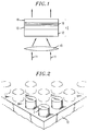
- FIG. 1 shows a cross-sectional view of a surface emitting laser.
- FIG. 2 shows a perspective view of a monolithic array of surface emitting lasers.
- FIG. 3(a) shows a reflectivity curve for the top distributed feedback mirror and FIG. 3(b) shows a reflectivity curve for the bottom distributed feedback mirror which are employed in the surface emitting laser of the present invention.
- FIG. 4 shows one embodiment of the surface emitting laser constructed in accordance with the present invention.
- FIG. 1 depicts an optically pumped surface emitting laser 2.
- a lens 10 directs incoming radiation through substrate 12 transparent to the radiation and thereafter through distributed feedback (DFB) mirror 13. If the substrate is not transparent to the radiation pumping is performed through the top of the laser 2 rather than through the substrate.
- the DFB mirror 13 is formed from alternating pairs of high and low refractive index material. Radiation is thereafter introduced into gain medium 16, which is formed from alternating layers of active material and barrier material.
- the laser is completed by DFB mirror 19 which is also formed from alternating pairs of high and low refractive index material. In the arrangement shown, the emitted lasing beam emerges vertically upward as shown by the arrows.
- FIG. 2 depicts a monolithic array of lasers 2 which are individually similar in composition to the laser shown in FIG. 1.
- the lasers 2 are all formed on a single substrate.
- Such arrays are useful as optical interconnects for integrated circuitry and as sources for optical pumping of solid state lasers.
- top and bottom mirrors 19 and 13 form a resonant cavity which supports a standing wave optical field at the designed wavelength of operation.
- the total thickness of the gain medium 16 is selected to be an integral multiple of one half the designed wavelength.
- the thickness of the active and barrier layers may be advantageously chosen so that the active layers coincide with the antinodes (i.e. intensity maxima) of the standing wave. This arrangement ensures that the active layers amplify the optical wave as efficiently as possible.
- the general structure and composition of the device shown in FIG. 1 is well-known to those skilled in art.
- the present invention does not depend on designation of appropriate lasing compositions.
- the selected materials must have properties known to be appropriate for operation.
- Active material must have a direct energy bandgap suitable for the desired radiation wavelength, and must otherwise be suitable for lasing.
- Barrier material a direct or indirect bandgap material, has a higher energy gap and serves to confine carriers within the active material.
- appropriate direct bandgap materials include the compound semiconductors such as selected materials of the III-V, the II-VI and the ternaries, quaternaries, as well as other complex compositions.
- Illustrative active material and barrier material pairs that may be employed include GaAs/ AlGaAs, In 0 .
- the device may be constructed by any appropriate technique such as MBE or MOCVD, for example.
- the device may also be constructed with a wedge-shaped laser cavity such as disclosed in U.S. Patent No. 4,395,769.
- FIG. 3 shows the reflectivity curve for the top mirror 19, which illustrates the mirror's reflectivity as a function of wavelength.
- the mirror 19 is configured as in the conventional manner to have maximum reflectivity at the designed wavelength of operation, which in the example shown in FIG. 3 is approximately 870 nm. This maximum reflectivity is approximately maintained over a prescribed bandwidth that encompasses the designed wavelength.
- the prescribed high reflectivity bandwidth is disturbed by a "notch" 30 defining a relatively narrow bandpass over which the reflectivity decreases substantially. That is, the notch 30 defines a bandwidth over which the mirror 19 transmits a significant amount of optical energy.
- Known surface emitting lasers employ top and bottom mirrors that have substantially identical normalized reflectivity curves such as shown in FIG. 3. That is, both mirrors typically employ the same high reflectivity bandwidth and both employ a "notch" at the same wavelength defining a region of higher transmission.
- This known configuration limits the efficiency of the laser because a significant portion of the pump energy that is not absorbed by the gain medium 16 will be transmitted through the notch in the bottom mirror and hence will be unavailable to induce additional population inversion.
- the top and bottom mirrors 13 and 19 are configured so that their reflectivity curves are shifted in wavelength relative to one another. That is, the reflectivity curves are displaced so that the notch in the top mirror is located at a different wavelength from the notch in the bottom mirror.
- This arrangement is indicated by the displacement of the reflectivity curve for the top mirror shown in FIG. 3(a) relative to the reflectivity curve for the bottom mirror shown in FIG. 3(b).
- the curves are displaced so that the notch in the top mirror is located at a wavelength at which the bottom mirror exhibits relatively high reflectivity.
- a substantial portion of the pump energy transmitted through the notch in the top mirror is reflected from the bottom mirror back up through the gain medium 16.
- the reflected pump energy then traverses the gain medium 16 for a second time, increasing its opportunity to induce population inversion. For example, if 50% of the pump energy is absorbed upon a single pass through the gain medium, then by increasing the reflectivity of the bottom mirror, 75 % of the pump energy will be absorbed upon traversing the gain medium 16 for a second time. By contrast, in known surface emitting lasers most of the pump energy has only a single opportunity to be absorbed by the gain medium 16.
- the optimal shift in the reflectivity curves for the top and bottom mirrors may be individually tailored for each particular device application. However some general considerations are appropriate independent of any particular application. For example, the relative shift should be sufficiently small so that that there is substantial overlap between the high reflectivity bandwidths of the top and bottom mirrors. This criteria ensures that a standing wave will be supported at the designed wavelength. For instance, a shift approximately equal to one-third of the high reflectivity bandwidth often will be appropriate. If the relative shift is too great one of the mirrors will have a reflectivity at the designed wavelength which is too low to efficiently support a standing wave.
- the gain medium 16 may be advantageously chosen so that approximately 50% of the pump energy is absorbed when traversing the gain medium for the first time. As noted above, this will cause approximately 75% of the pump energy to be absorbed after traversing the gain medium 16 twice. If substantially more than 50% of the pump energy is absorbed on the first pass, population inversion will occur in a nonuniform manner.
- FIG. 4 shows one particular embodiment of the inventive laser designed to operate at a wavelength of 870 nm.
- the top mirror 19 is formed from 25 pairs of alternating layers of Al 0.11 Ga 0.89 As (737 ⁇ ) and AlAs (625 ⁇ ) and the bottom mirror is formed from 29.5 pairs of Al 0.11 Ga 0.89 As (719 ⁇ ) and AlAs (608 ⁇ ).
- the gain medium is formed from three active layers of GaAs (609 ⁇ ) each separated by barrier layers of Al 0.11 Ga 0.89 As (625 ⁇ ).
- a barrier layer of Al 0.11 Ga 0.89 As (312 ⁇ ) is interposed between the active layers and each of the mirrors 13 and 19. The active layers are located at the antinodes of the standing wave supported between the mirrors 13 and 19 to maximize efficiency.
- the high reflectivity bandwidth of the bottom mirror 13 is shifted by approximately 14 nm relative to the top mirror 19.
- the mirrors 13 and 19 are also "unbalanced," as this term is defined in U.S. Patent No. 4,999,842, for example. That is, the bottom mirror 13 employs a greater number of alternating layers than the top mirror 19. As a result, the reflectivity of the bottom mirror 13 is greater than the reflectivity of the top mirror 19 at the design wavelength.
- the optical output beam will be emitted from the top mirror 19 because of its decreased reflectivity relative to the bottom mirror 13.
- the notch in the top mirror 19 is fully transmitting at the pump wavelength and is only 40-50 meV higher than the cavity mode wavelength, which is within the homogenous line width of the gain medium 16. As a result the laser is faster, more efficient with even coherent energy transfer, all of which decreases non-radiative losses.
Landscapes
- Physics & Mathematics (AREA)
- Condensed Matter Physics & Semiconductors (AREA)
- General Physics & Mathematics (AREA)
- Electromagnetism (AREA)
- Optics & Photonics (AREA)
- Semiconductor Lasers (AREA)
- Lasers (AREA)
Applications Claiming Priority (2)
| Application Number | Priority Date | Filing Date | Title |
|---|---|---|---|
| US417308 | 1995-04-05 | ||
| US08/417,308 US5513203A (en) | 1995-04-05 | 1995-04-05 | Surface emitting laser having improved pumping efficiency |
Publications (3)
| Publication Number | Publication Date |
|---|---|
| EP0742619A2 true EP0742619A2 (de) | 1996-11-13 |
| EP0742619A3 EP0742619A3 (de) | 1997-07-23 |
| EP0742619B1 EP0742619B1 (de) | 2000-10-04 |
Family
ID=23653431
Family Applications (1)
| Application Number | Title | Priority Date | Filing Date |
|---|---|---|---|
| EP96302076A Expired - Lifetime EP0742619B1 (de) | 1995-04-05 | 1996-03-26 | Oberflächenemittierender Laser mit verbessertem Wirkungsgrad |
Country Status (6)
| Country | Link |
|---|---|
| US (1) | US5513203A (de) |
| EP (1) | EP0742619B1 (de) |
| JP (1) | JP3121761B2 (de) |
| CA (1) | CA2171997C (de) |
| DE (1) | DE69610522T2 (de) |
| TW (1) | TW311295B (de) |
Families Citing this family (14)
| Publication number | Priority date | Publication date | Assignee | Title |
|---|---|---|---|---|
| US6243407B1 (en) | 1997-03-21 | 2001-06-05 | Novalux, Inc. | High power laser devices |
| US6341138B1 (en) | 1999-06-16 | 2002-01-22 | Gore Enterprise Holdings, Inc. | Constant temperature performance laser |
| US6625195B1 (en) * | 1999-07-20 | 2003-09-23 | Joseph Reid Henrichs | Vertical cavity surface emitting laser that uses intracavity degenerate four wave mixing to produce phase-conjugated and distortion free collimated laser light |
| WO2001078204A1 (en) * | 2000-04-07 | 2001-10-18 | The Government Of The United States Of America, As Represented By The Secretary Of The Navy | Optical pumping injection cavity for optically pumped devices |
| JP3829594B2 (ja) * | 2000-06-30 | 2006-10-04 | セイコーエプソン株式会社 | 素子実装方法と光伝送装置 |
| GB2369929A (en) * | 2000-12-08 | 2002-06-12 | Univ Southampton | Semiconductor laser device |
| DE10241192A1 (de) * | 2002-09-05 | 2004-03-11 | Osram Opto Semiconductors Gmbh | Optisch gepumpte strahlungsemittierende Halbleitervorrichtung und Verfahren zu deren Herstellung |
| TWI282650B (en) * | 2002-10-11 | 2007-06-11 | Eastman Kodak Co | Organic vertical cavity lasing devices having organic active region |
| GB2399941A (en) * | 2003-03-24 | 2004-09-29 | Univ Strathclyde | Vertical cavity semiconductor optical devices |
| GB2399942A (en) * | 2003-03-24 | 2004-09-29 | Univ Strathclyde | Vertical cavity semiconductor optical devices |
| US6836495B2 (en) * | 2003-05-07 | 2004-12-28 | Eastman Kodak Company | Vertical cavity laser including inorganic spacer layers |
| US6939012B2 (en) * | 2003-06-02 | 2005-09-06 | Eastman Kodak Company | Laser image projector |
| JP5214140B2 (ja) * | 2006-12-12 | 2013-06-19 | 浜松ホトニクス株式会社 | 半導体発光素子 |
| US8520713B2 (en) | 2010-11-19 | 2013-08-27 | Trilumina Corporation | Optical pumping of solid-state laser material using addressable laser array |
Family Cites Families (9)
| Publication number | Priority date | Publication date | Assignee | Title |
|---|---|---|---|---|
| US4395769A (en) * | 1981-03-03 | 1983-07-26 | Bell Telephone Laboratories, Incorporated | Tunable semiconductor laser |
| US4718070A (en) * | 1985-01-22 | 1988-01-05 | Massachusetts Institute Of Technology | Surface emitting diode laser |
| US4881236A (en) * | 1988-04-22 | 1989-11-14 | University Of New Mexico | Wavelength-resonant surface-emitting semiconductor laser |
| US4999842A (en) * | 1989-03-01 | 1991-03-12 | At&T Bell Laboratories | Quantum well vertical cavity laser |
| US5034344A (en) * | 1989-07-17 | 1991-07-23 | Bell Communications Research, Inc. | Method of making a surface emitting semiconductor laser |
| US4949350A (en) * | 1989-07-17 | 1990-08-14 | Bell Communications Research, Inc. | Surface emitting semiconductor laser |
| FR2681737A1 (fr) * | 1991-09-24 | 1993-03-26 | Thomson Csf | Source monofrequence de puissance a fibre optique. |
| US5206872A (en) * | 1991-11-01 | 1993-04-27 | At&T Bell Laboratories | Surface emitting laser |
| US5258990A (en) * | 1991-11-07 | 1993-11-02 | The United States Of America As Represented By The Secretary Of The United States Department Of Energy | Visible light surface emitting semiconductor laser |
-
1995
- 1995-04-05 US US08/417,308 patent/US5513203A/en not_active Expired - Lifetime
-
1996
- 1996-03-18 CA CA002171997A patent/CA2171997C/en not_active Expired - Fee Related
- 1996-03-26 DE DE69610522T patent/DE69610522T2/de not_active Expired - Fee Related
- 1996-03-26 EP EP96302076A patent/EP0742619B1/de not_active Expired - Lifetime
- 1996-04-04 JP JP08082430A patent/JP3121761B2/ja not_active Expired - Fee Related
- 1996-04-10 TW TW085104242A patent/TW311295B/zh active
Also Published As
| Publication number | Publication date |
|---|---|
| CA2171997A1 (en) | 1996-10-06 |
| US5513203A (en) | 1996-04-30 |
| EP0742619A3 (de) | 1997-07-23 |
| CA2171997C (en) | 1999-11-09 |
| JPH08340149A (ja) | 1996-12-24 |
| JP3121761B2 (ja) | 2001-01-09 |
| TW311295B (de) | 1997-07-21 |
| EP0742619B1 (de) | 2000-10-04 |
| DE69610522T2 (de) | 2001-03-22 |
| DE69610522D1 (de) | 2000-11-09 |
Similar Documents
| Publication | Publication Date | Title |
|---|---|---|
| US6434180B1 (en) | Vertical cavity surface emitting laser (VCSEL) | |
| US6148016A (en) | Integrated semiconductor lasers and photodetectors | |
| US5052016A (en) | Resonant-periodic-gain distributed-feedback surface-emitting semiconductor laser | |
| US4881236A (en) | Wavelength-resonant surface-emitting semiconductor laser | |
| US5513204A (en) | Long wavelength, vertical cavity surface emitting laser with vertically integrated optical pump | |
| US6252896B1 (en) | Long-Wavelength VCSEL using buried bragg reflectors | |
| EP1309051B1 (de) | Optischer Datenübertragungspfad enthaltend eine oberflächenemittierende Laserdiode mit Vertikalresonator und eine Photodiode mit Resonanzkavität | |
| US5513203A (en) | Surface emitting laser having improved pumping efficiency | |
| US7288421B2 (en) | Method for forming an optoelectronic device having an isolation layer | |
| US6771680B2 (en) | Electrically-pumped, multiple active region vertical-cavity surface-emitting laser (VCSEL) | |
| US5943359A (en) | Long wavelength VCSEL | |
| EP0892474B1 (de) | Intern optisch gepumpter, feldmodulierter, oberflächenemittierender Laser mit vertikalem Resonator | |
| US5883912A (en) | Long wavelength VCSEL | |
| JP2002523889A (ja) | 光励起外部ミラー垂直キャビティ半導体レーザー | |
| US6341138B1 (en) | Constant temperature performance laser | |
| US6782019B2 (en) | VCSEL with heat-spreading layer | |
| EP0785601B1 (de) | Sichtbares Licht emittierender VCSEL mit Hybridspiegel | |
| US8995482B1 (en) | High energy semiconductor laser | |
| US6560265B2 (en) | Method and apparatus for polarizing light in a VCSEL | |
| JP2002252418A (ja) | 光通信システム | |
| US6587492B2 (en) | Bipolar cascade arrow laser | |
| WO2000062384A1 (en) | Intra-cavity optically pumped vertical cavity surface emitting laser | |
| Kahle et al. | Membrane external-cavity surface-emitting lasers for high power broadband emission in the 1 µm range | |
| Schubert et al. | Extremely narrow spectral widths from resonant cavity light-emitting diodes (RCLEDs) suitable for wavelength-division multiplexing at 1.3 mu m and 1.55 mu m | |
| WO2007100341A2 (en) | Grazing incidence slab semiconductor laser system and method |
Legal Events
| Date | Code | Title | Description |
|---|---|---|---|
| PUAI | Public reference made under article 153(3) epc to a published international application that has entered the european phase |
Free format text: ORIGINAL CODE: 0009012 |
|
| AK | Designated contracting states |
Kind code of ref document: A2 Designated state(s): DE FR GB IT NL SE |
|
| PUAL | Search report despatched |
Free format text: ORIGINAL CODE: 0009013 |
|
| AK | Designated contracting states |
Kind code of ref document: A3 Designated state(s): DE FR GB IT NL SE |
|
| 17P | Request for examination filed |
Effective date: 19980108 |
|
| 17Q | First examination report despatched |
Effective date: 19980609 |
|
| GRAG | Despatch of communication of intention to grant |
Free format text: ORIGINAL CODE: EPIDOS AGRA |
|
| GRAG | Despatch of communication of intention to grant |
Free format text: ORIGINAL CODE: EPIDOS AGRA |
|
| GRAH | Despatch of communication of intention to grant a patent |
Free format text: ORIGINAL CODE: EPIDOS IGRA |
|
| GRAH | Despatch of communication of intention to grant a patent |
Free format text: ORIGINAL CODE: EPIDOS IGRA |
|
| GRAA | (expected) grant |
Free format text: ORIGINAL CODE: 0009210 |
|
| AK | Designated contracting states |
Kind code of ref document: B1 Designated state(s): DE FR GB IT NL SE |
|
| RIC1 | Information provided on ipc code assigned before grant |
Free format text: 7H 01S 5/183 A, 7H 01S 5/42 B, 7H 01S 3/091 B |
|
| ITF | It: translation for a ep patent filed | ||
| ET | Fr: translation filed | ||
| REF | Corresponds to: |
Ref document number: 69610522 Country of ref document: DE Date of ref document: 20001109 |
|
| PGFP | Annual fee paid to national office [announced via postgrant information from national office to epo] |
Ref country code: SE Payment date: 20001227 Year of fee payment: 6 |
|
| PGFP | Annual fee paid to national office [announced via postgrant information from national office to epo] |
Ref country code: FR Payment date: 20010222 Year of fee payment: 6 |
|
| PGFP | Annual fee paid to national office [announced via postgrant information from national office to epo] |
Ref country code: GB Payment date: 20010226 Year of fee payment: 6 |
|
| PGFP | Annual fee paid to national office [announced via postgrant information from national office to epo] |
Ref country code: NL Payment date: 20010312 Year of fee payment: 6 |
|
| PGFP | Annual fee paid to national office [announced via postgrant information from national office to epo] |
Ref country code: DE Payment date: 20010330 Year of fee payment: 6 |
|
| PLBE | No opposition filed within time limit |
Free format text: ORIGINAL CODE: 0009261 |
|
| STAA | Information on the status of an ep patent application or granted ep patent |
Free format text: STATUS: NO OPPOSITION FILED WITHIN TIME LIMIT |
|
| 26N | No opposition filed | ||
| REG | Reference to a national code |
Ref country code: GB Ref legal event code: IF02 |
|
| PG25 | Lapsed in a contracting state [announced via postgrant information from national office to epo] |
Ref country code: GB Free format text: LAPSE BECAUSE OF NON-PAYMENT OF DUE FEES Effective date: 20020326 |
|
| PG25 | Lapsed in a contracting state [announced via postgrant information from national office to epo] |
Ref country code: SE Free format text: LAPSE BECAUSE OF NON-PAYMENT OF DUE FEES Effective date: 20020327 |
|
| PG25 | Lapsed in a contracting state [announced via postgrant information from national office to epo] |
Ref country code: NL Free format text: LAPSE BECAUSE OF NON-PAYMENT OF DUE FEES Effective date: 20021001 Ref country code: DE Free format text: LAPSE BECAUSE OF NON-PAYMENT OF DUE FEES Effective date: 20021001 |
|
| EUG | Se: european patent has lapsed |
Ref document number: 96302076.3 |
|
| GBPC | Gb: european patent ceased through non-payment of renewal fee |
Effective date: 20020326 |
|
| PG25 | Lapsed in a contracting state [announced via postgrant information from national office to epo] |
Ref country code: FR Free format text: LAPSE BECAUSE OF NON-PAYMENT OF DUE FEES Effective date: 20021129 |
|
| NLV4 | Nl: lapsed or anulled due to non-payment of the annual fee |
Effective date: 20021001 |
|
| REG | Reference to a national code |
Ref country code: FR Ref legal event code: ST |
|
| PG25 | Lapsed in a contracting state [announced via postgrant information from national office to epo] |
Ref country code: IT Free format text: LAPSE BECAUSE OF NON-PAYMENT OF DUE FEES;WARNING: LAPSES OF ITALIAN PATENTS WITH EFFECTIVE DATE BEFORE 2007 MAY HAVE OCCURRED AT ANY TIME BEFORE 2007. THE CORRECT EFFECTIVE DATE MAY BE DIFFERENT FROM THE ONE RECORDED. Effective date: 20050326 |