EP0743379A1 - Vorrichtung für epitaxiales Aufwachsen aus der Gasphase - Google Patents
Vorrichtung für epitaxiales Aufwachsen aus der Gasphase Download PDFInfo
- Publication number
- EP0743379A1 EP0743379A1 EP96302927A EP96302927A EP0743379A1 EP 0743379 A1 EP0743379 A1 EP 0743379A1 EP 96302927 A EP96302927 A EP 96302927A EP 96302927 A EP96302927 A EP 96302927A EP 0743379 A1 EP0743379 A1 EP 0743379A1
- Authority
- EP
- European Patent Office
- Prior art keywords
- reaction vessel
- gas
- substrate
- vapor
- source gas
- Prior art date
- Legal status (The legal status is an assumption and is not a legal conclusion. Google has not performed a legal analysis and makes no representation as to the accuracy of the status listed.)
- Granted
Links
- 239000012808 vapor phase Substances 0.000 title claims abstract description 20
- 238000006243 chemical reaction Methods 0.000 claims abstract description 91
- 239000000758 substrate Substances 0.000 claims abstract description 61
- 239000010409 thin film Substances 0.000 claims abstract description 38
- 238000010438 heat treatment Methods 0.000 claims abstract description 13
- 230000002093 peripheral effect Effects 0.000 claims abstract description 10
- 239000013078 crystal Substances 0.000 claims abstract description 9
- 239000007789 gas Substances 0.000 claims description 90
- 239000012495 reaction gas Substances 0.000 claims description 3
- 230000007704 transition Effects 0.000 abstract description 10
- 230000007423 decrease Effects 0.000 abstract description 7
- 239000004065 semiconductor Substances 0.000 abstract description 5
- 239000012535 impurity Substances 0.000 description 10
- 238000001947 vapour-phase growth Methods 0.000 description 9
- 238000011144 upstream manufacturing Methods 0.000 description 7
- 239000012159 carrier gas Substances 0.000 description 6
- 239000010408 film Substances 0.000 description 5
- QGZKDVFQNNGYKY-UHFFFAOYSA-N Ammonia Chemical compound N QGZKDVFQNNGYKY-UHFFFAOYSA-N 0.000 description 4
- ZOXJGFHDIHLPTG-UHFFFAOYSA-N Boron Chemical compound [B] ZOXJGFHDIHLPTG-UHFFFAOYSA-N 0.000 description 4
- 229910052796 boron Inorganic materials 0.000 description 4
- UFHFLCQGNIYNRP-UHFFFAOYSA-N Hydrogen Chemical compound [H][H] UFHFLCQGNIYNRP-UHFFFAOYSA-N 0.000 description 3
- XUIMIQQOPSSXEZ-UHFFFAOYSA-N Silicon Chemical compound [Si] XUIMIQQOPSSXEZ-UHFFFAOYSA-N 0.000 description 3
- 230000003247 decreasing effect Effects 0.000 description 3
- 230000007547 defect Effects 0.000 description 3
- 238000010586 diagram Methods 0.000 description 3
- 239000000203 mixture Substances 0.000 description 3
- 229910052710 silicon Inorganic materials 0.000 description 3
- 239000010703 silicon Substances 0.000 description 3
- RWSOTUBLDIXVET-UHFFFAOYSA-N Dihydrogen sulfide Chemical compound S RWSOTUBLDIXVET-UHFFFAOYSA-N 0.000 description 2
- 229910001218 Gallium arsenide Inorganic materials 0.000 description 2
- XYFCBTPGUUZFHI-UHFFFAOYSA-N Phosphine Chemical compound P XYFCBTPGUUZFHI-UHFFFAOYSA-N 0.000 description 2
- RBFQJDQYXXHULB-UHFFFAOYSA-N arsane Chemical compound [AsH3] RBFQJDQYXXHULB-UHFFFAOYSA-N 0.000 description 2
- 230000000694 effects Effects 0.000 description 2
- 238000005259 measurement Methods 0.000 description 2
- 238000000034 method Methods 0.000 description 2
- 229910021421 monocrystalline silicon Inorganic materials 0.000 description 2
- 229910000069 nitrogen hydride Inorganic materials 0.000 description 2
- 239000002245 particle Substances 0.000 description 2
- 238000007086 side reaction Methods 0.000 description 2
- 238000003756 stirring Methods 0.000 description 2
- VYPSYNLAJGMNEJ-UHFFFAOYSA-N Silicium dioxide Chemical compound O=[Si]=O VYPSYNLAJGMNEJ-UHFFFAOYSA-N 0.000 description 1
- 229910021529 ammonia Inorganic materials 0.000 description 1
- 229910000070 arsenic hydride Inorganic materials 0.000 description 1
- XOYLJNJLGBYDTH-UHFFFAOYSA-M chlorogallium Chemical compound [Ga]Cl XOYLJNJLGBYDTH-UHFFFAOYSA-M 0.000 description 1
- 230000000052 comparative effect Effects 0.000 description 1
- 150000001875 compounds Chemical class 0.000 description 1
- 238000010276 construction Methods 0.000 description 1
- 239000002826 coolant Substances 0.000 description 1
- 230000008021 deposition Effects 0.000 description 1
- 239000002019 doping agent Substances 0.000 description 1
- UPWPDUACHOATKO-UHFFFAOYSA-K gallium trichloride Chemical compound Cl[Ga](Cl)Cl UPWPDUACHOATKO-UHFFFAOYSA-K 0.000 description 1
- 239000001257 hydrogen Substances 0.000 description 1
- 229910052739 hydrogen Inorganic materials 0.000 description 1
- 229910000037 hydrogen sulfide Inorganic materials 0.000 description 1
- 230000006698 induction Effects 0.000 description 1
- 230000014759 maintenance of location Effects 0.000 description 1
- 229910000073 phosphorus hydride Inorganic materials 0.000 description 1
- 238000002360 preparation method Methods 0.000 description 1
- ZDHXKXAHOVTTAH-UHFFFAOYSA-N trichlorosilane Chemical compound Cl[SiH](Cl)Cl ZDHXKXAHOVTTAH-UHFFFAOYSA-N 0.000 description 1
- 239000005052 trichlorosilane Substances 0.000 description 1
Images



Classifications
-
- C—CHEMISTRY; METALLURGY
- C30—CRYSTAL GROWTH
- C30B—SINGLE-CRYSTAL GROWTH; UNIDIRECTIONAL SOLIDIFICATION OF EUTECTIC MATERIAL OR UNIDIRECTIONAL DEMIXING OF EUTECTOID MATERIAL; REFINING BY ZONE-MELTING OF MATERIAL; PRODUCTION OF A HOMOGENEOUS POLYCRYSTALLINE MATERIAL WITH DEFINED STRUCTURE; SINGLE CRYSTALS OR HOMOGENEOUS POLYCRYSTALLINE MATERIAL WITH DEFINED STRUCTURE; AFTER-TREATMENT OF SINGLE CRYSTALS OR A HOMOGENEOUS POLYCRYSTALLINE MATERIAL WITH DEFINED STRUCTURE; APPARATUS THEREFOR
- C30B25/00—Single-crystal growth by chemical reaction of reactive gases, e.g. chemical vapour-deposition growth
- C30B25/02—Epitaxial-layer growth
- C30B25/14—Feed and outlet means for the gases; Modifying the flow of the reactive gases
-
- Y—GENERAL TAGGING OF NEW TECHNOLOGICAL DEVELOPMENTS; GENERAL TAGGING OF CROSS-SECTIONAL TECHNOLOGIES SPANNING OVER SEVERAL SECTIONS OF THE IPC; TECHNICAL SUBJECTS COVERED BY FORMER USPC CROSS-REFERENCE ART COLLECTIONS [XRACs] AND DIGESTS
- Y10—TECHNICAL SUBJECTS COVERED BY FORMER USPC
- Y10T—TECHNICAL SUBJECTS COVERED BY FORMER US CLASSIFICATION
- Y10T117/00—Single-crystal, oriented-crystal, and epitaxy growth processes; non-coating apparatus therefor
- Y10T117/10—Apparatus
- Y10T117/1016—Apparatus with means for treating single-crystal [e.g., heat treating]
Definitions
- This invention relates to an apparatus for the vapor-phase growth of a thin film on a semiconductor single crystal substrate.
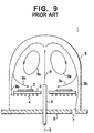
- a susceptor 3 for loading thereon a semiconductor single crystal substrate(s) 2 (hereinafter referred to briefly as “substrate(s)") is rotatably arranged horizontally in a reaction vessel 8 of the shape of a bell jar set in place on a base plate 6, and a source gas 9 supplied through a gas nozzle 5 provided in the central part of the susceptor 3 is introduced into the reaction vessel 8 while the substrate(s) 2 is heated by the use of a high-frequency induction heating coil 4 to effect growth of a thin film on the substrate(s) 2.
- the gas nozzle 5 provided in the central part of the reaction vessel 8 is so constructed as to introduce the source gas 9 horizontally toward the periphery, the source gas 9 flows in a scattered manner out of the gas nozzle 5 and it is consumed in proportion as the growth of the thin film on the surface of the substrate(s) 2 advances.
- the concentration of the source gas 9 over the substrate(s) 2 decreases and the growth rate of the thin layer thereon decreases in accordance as the distance from the central part of the reaction vessel 8 increases.
- This forced convection and a natural convection formed by the difference of temperature between the susceptor 3 and the reaction vessel 8 are joined to produce a convection 9a.
- the reaction ambience is stirred at an increased rate by the convection 9a formed in the upper interior part of the reaction vessel 8, and the concentration of the source gas 9 can be rendered uniform by virtue of the stirring force of the convection 9a.
- the source gas 9 when supplied in the upward direction in the reaction vessel 8 of an increased height, the gas flows slowly near the main surface of the substrate(s) 2 and the stagnant layer of gas becomes thicker.
- the atmosphere of the main surface of the substrate(s) 2 is affected strongly by the phenomenon of auto-doping arising from the substrate(s) itself so that the transition width, namely, the width of the part in which the concentration of impurities varies at the interface between a substrate and a thin film, tends to increase.
- This invention produced in view of the prior art mentioned above, has an object thereof the provision of an apparatus for the vapor-phase epitaxial growth of a thin film which simultaneously permits the transition width to be decreased and the thickness of the thin film to be grown uniformly.
- An apparatus of this invention is characterized by comprising a reaction vessel of a flat shape, gas supply means for feeding a source gas from the peripheral part of the reaction vessel, a susceptor for holding a semiconductor single crystal substrate(s) substantially horizontally, heating means, and a reaction gas outlet provided in the central part of an upper wall of the reaction vessel.
- the reaction vessel is formed in the shape of a flat cylinder, and the gas supply means is provided with a plurality of gas supply inlets so adapted as to feed a source gas in the circular direction of the reaction vessel.
- the gas supply inlets preferably are spaced with an egual angular pitch as symmetrized around the axis of the reaction vessel. Further, the gas supply inlets are so arranged that the source gas generate a horizontal rotary flow in the reaction vessel.
- a substrate 12 is first set in place substantially horizontally on a susceptor (supporting member) 13 in a reaction vessel 18 as shown in Fig. 1 and Fig. 2 and then the substrate 12 is heated to a required temperature with heating means (infrared heating lamp) 14 while a carrier gas such as hydrogen is continuously fed thereto.
- heating means infrared heating lamp
- a source gas 19 When a source gas 19 is subsequently introduced with the carrier gas in a horizontal direction from the peripheral part of the reaction vessel 18 of the shape of a flat cylinder, the source gas 19 flows over the substrate 12 substantially horizontally in the direction of a gas outlet 11. The source gas 19 thereafter is caused to form a slightly upward flow by the buoyant force due to heating. But, this flow of the source gas quickly goes out upward in the vertical direction through the gas outlet 11 provided in an upper wall of the reaction vessel 18 before it forms a vortex.
- the concentration of the source gas 19 fed from gas supply inlets 16 located at the peripheral part of the reaction vessel 18 decreases along the direction of gas flow toward the central part according to the advance of the consumption of the source for the epitaxial growth.
- the flow rate of the source gas 19, however, increases as the distance to the central part decreases because the source gas 19 gathers from the peripheral part of the reaction vessel to the central part.
- the amount of the source itself to be fed per unit time is practically uniform throughout the entire main surface of the substrate 12 and, consequently, the distribution of the epitaxial growth rate can be uniformized throughout the entire area of the substrate 12.
- the reaction vessel 18 When the reaction vessel 18 is formed in the shape of a flat cylinder and the plurality of gas feed inlets 16 as gas feed means are so provided as to feed the source gas 19 in the circular direction of the reaction vessel 18, the source gas forms a horizontal rotary flow inside the reaction vessel, resulting the concentration of the source gas 19 can be uniformized by virtue of the stirring force generated by the horizontal rotary current mentioned above, and the gas flow can be smooth so that otherwise possible occurrence of the convection vortex of the source gas 19 can be precluded.
- the gas flow near the gas supply inlets is further smooth.
- the distribution of thickness of the thin film deposited by the vapor-phase epitaxial growth can be further improved.
- Fig. 1 is a schematic cross section of the reaction vessel 18, and Fig. 2 is a schematic plan view thereof.
- the reaction vessel 18 is made of transparent quartz glass, formed in the shape of a flat cylinder consisting of a cylindrical side wall 18a, a disk-shape upper wall 18b, and a disk-shape lower wall 18c, and set in place horizontally.
- the inner height of the reaction vessel 18, namely the distance between the inner surface of the upper wall 18b and the inner surface of the lower surface 18c, is set in the range of 10 mm to 20 mm and the inside diameter of the side wall 18a is set in the range of 250 mm to 400 mm.
- a reaction vessel 18 having an inner height of 15 mm and an inside diameter of 300 mm was used.
- a susceptor 13 for supporting a substrate 12 in a substantially horizontal direction is set in place in the reaction vessel 18 and a disk-shape substrate 12 having a diameter of 200 mm is held on the susceptor 13.
- a set of infrared heating lamp 14 is installed outside the reaction vessel 18. With the radiant heat from the infrared heating lamp 14, the substrate 12 and the susceptor 13 in the reaction vessel 18 are heated. The outer wall of the reaction vessel 18 is cooled with such a cooling medium as air which is omitted from illustration.
- a gas outlet tube 17 having an inner diameter of 20 mm is projected perpendicularly to the upper wall 18b so as to allow upward discharge of the reaction gas in the vertical direction through the gas outlet 11.
- the four supply nozzles 15 mentioned above accord with a same specification. They are invariably set at a same angle ⁇ (indicated in the plan view of Fig. 2) of 75° so as to supply the source gas 19 in the circular direction of the reaction vessel 18.
- the supply nozzles 15 have an inside diameter of 10 mm so that the total of the opening areas occupied by the four supply nozzles 15 for introducing the gas is equal to the opening area of the gas outlet tube 17.
- Trichlorosilane fed as a source gas 19 at a rate of 5 g/minute and hydrogen gas fed as a carrier gas at a rate of 100 liters/minute are mixed and the mixed gas is introduced evenly through the four supply nozzles 15 into the reaction vessel 18.
- the source gas 19 introduced with the carrier gas from the peripheral part of the reaction vessel 18 being fed in the circular direction of the reaction vessel 18 in the shape of a cylinder flows over the substrate 12 while generating a horizontal rotary flow, and after playing the role of effecting vapor-phase epitaxial growth on the substrate, goes out upward through the gas outlet 11.
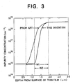
- a thin film of silicon doped with boron having an impurity concentration of 1 x 10 15 cm -3 was grown in a thickness of 1.5 pm by a vapor-phase epitaxial growth at a temperature of 1100°C in one minute.
- the impurity concentration of the thin film was analyzed in the direction of depth. The profile of concentration thus obtained is shown in Fig. 3.
- a thin film of silicon doped with boron having an impurity concentration of 1 x 10 15 cm -3 was grown in a thickness of 1.5 ⁇ m by a vapor-phase epitaxial growth at a temperature of 1100°C in one minute, in the same manner as in the preceding example.
- the impurity concentration of the thin film was analyzed in the direction of depth. The profile of concentration thus obtained is additionally shown in Fig. 3.
- transition width W2 obtained by the epitaxial growth in the reaction vessel 18 of the vapor-phase growth apparatus 10 according to this invention is 0.8 pm
- transition width W1 obtained by the epitaxial growth in the conventional vapor-phase growth apparatus 1 is 1.3 pm. This fact indicates that this invention accomplishes a notable improvement of the transition witdth
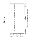
- Fig. 4 shows the growth rate profile direction of diameter of the substrate 12 in the reaction vessel 18 according to this invention, obtained by thin film growth on the substrate 12.
- the growth rate is obtained by dividing the thickness at each point by the growth time.
- the use of the vapor-phase growth apparatus of this invention attains a notable improvement in the transition width, and at the same time, enables a thin film to be formed in a uniform thickness and a uniform growth rate distribution throughout the entire main surface of the substrate 12.
- Example 1 since the gas outlet tube 17 is positioned above the substrate 12, a possibility is suspected that particles arising from a side reaction of the vapor-phase epitaxial growth adhere to the gas outlet tube 17, fall therefrom onto the substrate 12, and give rise to a defect of the surface of the formed thin film. In actuality, however, the surface of the thin film is not found to have any surface defects such as a protruding defect.
- Example 1 cited above has been depicted as a case of loading one substrate 12 having a diameter of 200 mm in the reaction vessel 18. It is naturally permissible to have a plurality of substrate(s) of a smaller diameter simultaneously loaded in the reaction vessel 18 for the vapor-phase epitaxial growth.
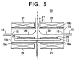
- Fig. 5 portrays a plurality of substrate(s) 22 loaded for vapor-phase epitaxial growth.
- 20 stands for a vapor-phase growth apparatus
- 21 for a resistance heating furnace
- 29 for a source gas.
- like parts found in Fig. 1 are denoted by like reference numerals.
- This method of growth is particularly effective when thin films such as GaAs, GaP, and GaAsP are grown on such substrate(s) 22 made of GaAs, GaP, and GaAsP, because those substrate(s) 22 have smaller diameters than the substrate(s) made of silicon.
- the reaction vessel 18 of Fig. 5 is identical in shape and construction with the reaction vessel 18 of Fig. 1. However it is different from the latter reaction vessel in respect that the resistance heating furnace 21 is so prepared as to encircle the upper wall 18b and the lower wall 18c of the reaction vessel 18.
- the reaction vessels 18 has an inside diameter of 250 mm and an inner height of 20 mm.
- the preparation of the resistance heating furnace 21 in the manner described above is for the purpose of suppressing the deposition on the wall of the reaction vessel 18 by heating the walls.
- reaction vessel 18 of Fig. 5 six substrate(s) made of GaP of 50 mm in diameter are set in place concentrically with the side wall 18a of the reaction vessel 18.
- a mixed gas consisting of gallium chloride (GaCl), arsine (AsH 3 ) and phosphine (PH 3 ) as the source gas 29, ammonia (NH 3 ) and hydrogen sulfide (H 2 S) as the dopant and hydrogen gas as a carrier gas were supplied at a flow rate of 14 liters/minute.
- This mixed gas contains GaCl at a rate of 110 ml/minute, ASH 3 at a rate of 26 ml/minute, PH 3 at a rate of 48 ml/minute, NH 3 at a rate of 600 ml/minute, and a very minute amount (several ml/minute) of H 2 S.
- an n-type GaASP layer having a film thickness of about 40 ⁇ m was formed at a growth rate of 0.2 ⁇ m/minute.
- About 60% of the film thickness of 40 ⁇ m serves as a composition grading layer for allowing gradual change of the crystal composition from GaP of the substrate to GaASP.
- the thickness of the thin film obtained by the epitaxial growth mentioned above was measured from the upstream side to the downstream side of the flow of the source gas.
- the results are shown in Fig. 8.
- the horizontal axis is a scale of the position of measurement of film thickness on the substrate
- the vertical axis is a scale of the thickness of thin film obtained by the measurement.
- the point "0 mm (upstream side)" on the horizontal axis represents the peripheral part A of the substrate nearest to the side wall 18a of the reaction vessel 18
- the point "25 mm (central part)” represents the central part B of the substrate
- the point "50 mm (downstream side)” represents the peripheral terminal part C of the substrate nearest to the central part of the reaction vessel 18.
- a susceptor 33 was set in place in a reaction vessel 30 designed for the conventional growth of a thin film of compound semiconductor single crystal shown in Fig. 7, and six substrate(s) 22 were loaded each in the upper and the lower zone of the susceptor 33, and the source gas 29 was supplied in a downstream direction to effect vapor-phase epitaxial growth.
- the components, composition, and flow volume per substrate of the source gas 29 were set equal to those of Example 2 mentioned above.
- the thickness of the thin film obtained by the vapor-phase epitaxial growth in the conventional reaction vessel 30 mentioned above was measured from the upstream side to the downward side of the flow of the source gas.
- the results are additionally shown in Fig. 8.
- the point "0 mm (upstream side)” represents the upper peripheral part D of the substrate
- the point "25 mm (central part)” represents the central part E of the substrate
- the point "50 mm (downstream side)” represents the lower terminal part F of the substrate.
- the thickness of the thin film gradually decreases from the upstream to the downstream side, specifically from the thickness of about 60 ⁇ m at the point D on the upstream side to the thickness of about 37 pm at the point F on the downstream side.
- the thickness of epitaxial growth shows a large gradient.
- the maximum thickness of the thin film is about 45 ⁇ m and the minimum thickness thereof about 38 ⁇ m, indicating that the distribution of thickness of the thin film is appreciably uniform throughout the entire area of the substrate.
- the distribution of the epitaxial growth rate and the distribution of the film thickness can be uniform throughout the entire area of the substrate because the amount of the source supplied per unit time can be rendered practically uniform throughout the entire main surface of the substrate.
- this invention attains a decrease in the transition width, and at the same time, enables the thin film to be formed in a uniform thickness on the substrate.
Landscapes
- Chemical & Material Sciences (AREA)
- Chemical Kinetics & Catalysis (AREA)
- General Chemical & Material Sciences (AREA)
- Engineering & Computer Science (AREA)
- Crystallography & Structural Chemistry (AREA)
- Materials Engineering (AREA)
- Metallurgy (AREA)
- Organic Chemistry (AREA)
- Chemical Vapour Deposition (AREA)
Applications Claiming Priority (3)
| Application Number | Priority Date | Filing Date | Title |
|---|---|---|---|
| JP12712295 | 1995-04-27 | ||
| JP7127122A JPH08306632A (ja) | 1995-04-27 | 1995-04-27 | 気相エピタキシャル成長装置 |
| JP127122/95 | 1995-04-27 |
Publications (2)
| Publication Number | Publication Date |
|---|---|
| EP0743379A1 true EP0743379A1 (de) | 1996-11-20 |
| EP0743379B1 EP0743379B1 (de) | 1999-07-07 |
Family
ID=14952158
Family Applications (1)
| Application Number | Title | Priority Date | Filing Date |
|---|---|---|---|
| EP96302927A Expired - Lifetime EP0743379B1 (de) | 1995-04-27 | 1996-04-26 | Vorrichtung für epitaxiales Aufwachsen aus der Gasphase |
Country Status (4)
| Country | Link |
|---|---|
| US (1) | US5672204A (de) |
| EP (1) | EP0743379B1 (de) |
| JP (1) | JPH08306632A (de) |
| DE (1) | DE69603126T2 (de) |
Cited By (11)
| Publication number | Priority date | Publication date | Assignee | Title |
|---|---|---|---|---|
| WO2003048430A1 (de) * | 2001-11-27 | 2003-06-12 | Osram Opto Semiconductors Gmbh | Vorrichtung und verfahren zum herstellen, abtragen oder behandeln von schichten auf einem substrat |
| EP1573779A4 (de) * | 2001-04-10 | 2006-11-15 | Tokyo Electron Ltd | Hochdruckverarbeitungskammer für ein halbleitersubstrat mit strömungsverbesserungsmerkmalen |
| US7163380B2 (en) | 2003-07-29 | 2007-01-16 | Tokyo Electron Limited | Control of fluid flow in the processing of an object with a fluid |
| US7186093B2 (en) | 2004-10-05 | 2007-03-06 | Tokyo Electron Limited | Method and apparatus for cooling motor bearings of a high pressure pump |
| US7225820B2 (en) | 2003-02-10 | 2007-06-05 | Tokyo Electron Limited | High-pressure processing chamber for a semiconductor wafer |
| US7255772B2 (en) | 2000-07-26 | 2007-08-14 | Tokyo Electron Limited | High pressure processing chamber for semiconductor substrate |
| US7270137B2 (en) | 2003-04-28 | 2007-09-18 | Tokyo Electron Limited | Apparatus and method of securing a workpiece during high-pressure processing |
| US7387868B2 (en) | 2002-03-04 | 2008-06-17 | Tokyo Electron Limited | Treatment of a dielectric layer using supercritical CO2 |
| EP1874979A4 (de) * | 2005-04-22 | 2008-11-05 | Beneq Oy | Reaktor |
| US7494107B2 (en) | 2005-03-30 | 2009-02-24 | Supercritical Systems, Inc. | Gate valve for plus-atmospheric pressure semiconductor process vessels |
| US7767145B2 (en) | 2005-03-28 | 2010-08-03 | Toyko Electron Limited | High pressure fourier transform infrared cell |
Families Citing this family (34)
| Publication number | Priority date | Publication date | Assignee | Title |
|---|---|---|---|---|
| US6410090B1 (en) | 1998-09-29 | 2002-06-25 | Applied Materials, Inc. | Method and apparatus for forming insitu boron doped polycrystalline and amorphous silicon films |
| US6748960B1 (en) | 1999-11-02 | 2004-06-15 | Tokyo Electron Limited | Apparatus for supercritical processing of multiple workpieces |
| KR100744888B1 (ko) | 1999-11-02 | 2007-08-01 | 동경 엘렉트론 주식회사 | 소재를 초임계 처리하기 위한 장치 및 방법 |
| US6428847B1 (en) * | 2000-10-16 | 2002-08-06 | Primaxx, Inc. | Vortex based CVD reactor |
| US20040028810A1 (en) * | 2000-10-16 | 2004-02-12 | Primaxx, Inc. | Chemical vapor deposition reactor and method for utilizing vapor vortex |
| US20030047138A1 (en) * | 2001-09-11 | 2003-03-13 | Ceramoptec Industries, Inc. | Spiral gas flow plasma reactor |
| EP1432844B1 (de) * | 2001-09-29 | 2018-11-21 | Cree, Inc. | Vorrichtung zur invertierten chemischen gasphasenabscheidung |
| US20040040660A1 (en) * | 2001-10-03 | 2004-03-04 | Biberger Maximilian Albert | High pressure processing chamber for multiple semiconductor substrates |
| US7001468B1 (en) | 2002-02-15 | 2006-02-21 | Tokyo Electron Limited | Pressure energized pressure vessel opening and closing device and method of providing therefor |
| US7021635B2 (en) * | 2003-02-06 | 2006-04-04 | Tokyo Electron Limited | Vacuum chuck utilizing sintered material and method of providing thereof |
| US7077917B2 (en) | 2003-02-10 | 2006-07-18 | Tokyo Electric Limited | High-pressure processing chamber for a semiconductor wafer |
| JP2004288899A (ja) * | 2003-03-24 | 2004-10-14 | Tokyo Electron Ltd | 成膜方法および基板処理装置 |
| US20050035514A1 (en) * | 2003-08-11 | 2005-02-17 | Supercritical Systems, Inc. | Vacuum chuck apparatus and method for holding a wafer during high pressure processing |
| US7250374B2 (en) | 2004-06-30 | 2007-07-31 | Tokyo Electron Limited | System and method for processing a substrate using supercritical carbon dioxide processing |
| US7307019B2 (en) | 2004-09-29 | 2007-12-11 | Tokyo Electron Limited | Method for supercritical carbon dioxide processing of fluoro-carbon films |
| US7491036B2 (en) | 2004-11-12 | 2009-02-17 | Tokyo Electron Limited | Method and system for cooling a pump |
| US7434590B2 (en) | 2004-12-22 | 2008-10-14 | Tokyo Electron Limited | Method and apparatus for clamping a substrate in a high pressure processing system |
| US7140393B2 (en) | 2004-12-22 | 2006-11-28 | Tokyo Electron Limited | Non-contact shuttle valve for flow diversion in high pressure systems |
| US7435447B2 (en) | 2005-02-15 | 2008-10-14 | Tokyo Electron Limited | Method and system for determining flow conditions in a high pressure processing system |
| US7291565B2 (en) | 2005-02-15 | 2007-11-06 | Tokyo Electron Limited | Method and system for treating a substrate with a high pressure fluid using fluorosilicic acid |
| US7380984B2 (en) | 2005-03-28 | 2008-06-03 | Tokyo Electron Limited | Process flow thermocouple |
| JP2006303152A (ja) * | 2005-04-20 | 2006-11-02 | Fuji Electric Holdings Co Ltd | エピタキシャル成膜装置およびエピタキシャル成膜方法 |
| US7789971B2 (en) | 2005-05-13 | 2010-09-07 | Tokyo Electron Limited | Treatment of substrate using functionalizing agent in supercritical carbon dioxide |
| US7524383B2 (en) | 2005-05-25 | 2009-04-28 | Tokyo Electron Limited | Method and system for passivating a processing chamber |
| JP2009093711A (ja) * | 2007-10-04 | 2009-04-30 | Hoya Corp | 磁気記録媒体の製造方法および磁気記録媒体 |
| US8298338B2 (en) | 2007-12-26 | 2012-10-30 | Samsung Electronics Co., Ltd. | Chemical vapor deposition apparatus |
| US8291857B2 (en) * | 2008-07-03 | 2012-10-23 | Applied Materials, Inc. | Apparatuses and methods for atomic layer deposition |
| TW201246297A (en) * | 2011-04-07 | 2012-11-16 | Veeco Instr Inc | Metal-organic vapor phase epitaxy system and process |
| KR102413455B1 (ko) * | 2015-01-02 | 2022-06-27 | 어플라이드 머티어리얼스, 인코포레이티드 | 처리 챔버 |
| CA2974387A1 (en) * | 2016-08-30 | 2018-02-28 | Rolls-Royce Corporation | Swirled flow chemical vapor deposition |
| JP6698489B2 (ja) * | 2016-09-26 | 2020-05-27 | 株式会社Screenホールディングス | 基板処理装置および基板処理方法 |
| JP2020126881A (ja) * | 2019-02-01 | 2020-08-20 | 東京エレクトロン株式会社 | 基板処理装置およびクリーニング方法 |
| JP2022107873A (ja) * | 2021-01-12 | 2022-07-25 | 東京エレクトロン株式会社 | 基板処理装置及びクリーニング方法 |
| JP2025003184A (ja) * | 2023-06-23 | 2025-01-09 | 株式会社Screenホールディングス | 基板処理装置および基板処理方法 |
Citations (4)
| Publication number | Priority date | Publication date | Assignee | Title |
|---|---|---|---|---|
| US3293074A (en) * | 1963-11-05 | 1966-12-20 | Siemens Ag | Method and apparatus for growing monocrystalline layers on monocrystalline substrates of semiconductor material |
| FR1518843A (fr) * | 1967-02-13 | 1968-03-29 | Radiotechnique Coprim Rtc | Dispositif pour le dépôt de couches minces sur des supports semi-conducteurs |
| US4033286A (en) * | 1976-07-12 | 1977-07-05 | California Institute Of Technology | Chemical vapor deposition reactor |
| EP0366173A1 (de) * | 1988-10-14 | 1990-05-02 | Laboratoires D'electronique Philips | Epitaxiereaktor mit einem verbesserten Gassammler |
Family Cites Families (4)
| Publication number | Priority date | Publication date | Assignee | Title |
|---|---|---|---|---|
| US4323031A (en) * | 1979-04-30 | 1982-04-06 | Alan Kaplan | Crystal plating apparatus |
| US4512283A (en) * | 1982-02-01 | 1985-04-23 | Texas Instruments Incorporated | Plasma reactor sidewall shield |
| JPH01189692A (ja) * | 1988-01-26 | 1989-07-28 | Toshiba Corp | 登録文字種のドットマトリクス変換方法 |
| US5531834A (en) * | 1993-07-13 | 1996-07-02 | Tokyo Electron Kabushiki Kaisha | Plasma film forming method and apparatus and plasma processing apparatus |
-
1995
- 1995-04-27 JP JP7127122A patent/JPH08306632A/ja active Pending
-
1996
- 1996-04-25 US US08/637,576 patent/US5672204A/en not_active Expired - Fee Related
- 1996-04-26 DE DE69603126T patent/DE69603126T2/de not_active Expired - Fee Related
- 1996-04-26 EP EP96302927A patent/EP0743379B1/de not_active Expired - Lifetime
Patent Citations (4)
| Publication number | Priority date | Publication date | Assignee | Title |
|---|---|---|---|---|
| US3293074A (en) * | 1963-11-05 | 1966-12-20 | Siemens Ag | Method and apparatus for growing monocrystalline layers on monocrystalline substrates of semiconductor material |
| FR1518843A (fr) * | 1967-02-13 | 1968-03-29 | Radiotechnique Coprim Rtc | Dispositif pour le dépôt de couches minces sur des supports semi-conducteurs |
| US4033286A (en) * | 1976-07-12 | 1977-07-05 | California Institute Of Technology | Chemical vapor deposition reactor |
| EP0366173A1 (de) * | 1988-10-14 | 1990-05-02 | Laboratoires D'electronique Philips | Epitaxiereaktor mit einem verbesserten Gassammler |
Non-Patent Citations (1)
| Title |
|---|
| FRIJLINK P M ET AL: "LAYER UNIFORMITY IN A MULTIWAFER MOVPE REACTOR FOR III-V COMPOUNDS", JOURNAL OF CRYSTAL GROWTH, vol. 107, no. 1 / 04, 1 January 1991 (1991-01-01), pages 166 - 174, XP000246591 * |
Cited By (12)
| Publication number | Priority date | Publication date | Assignee | Title |
|---|---|---|---|---|
| US7255772B2 (en) | 2000-07-26 | 2007-08-14 | Tokyo Electron Limited | High pressure processing chamber for semiconductor substrate |
| EP1573779A4 (de) * | 2001-04-10 | 2006-11-15 | Tokyo Electron Ltd | Hochdruckverarbeitungskammer für ein halbleitersubstrat mit strömungsverbesserungsmerkmalen |
| CN100392796C (zh) * | 2001-04-10 | 2008-06-04 | 东京毅力科创株式会社 | 包含流量增强特征的半导体衬底高压加工室 |
| WO2003048430A1 (de) * | 2001-11-27 | 2003-06-12 | Osram Opto Semiconductors Gmbh | Vorrichtung und verfahren zum herstellen, abtragen oder behandeln von schichten auf einem substrat |
| US7387868B2 (en) | 2002-03-04 | 2008-06-17 | Tokyo Electron Limited | Treatment of a dielectric layer using supercritical CO2 |
| US7225820B2 (en) | 2003-02-10 | 2007-06-05 | Tokyo Electron Limited | High-pressure processing chamber for a semiconductor wafer |
| US7270137B2 (en) | 2003-04-28 | 2007-09-18 | Tokyo Electron Limited | Apparatus and method of securing a workpiece during high-pressure processing |
| US7163380B2 (en) | 2003-07-29 | 2007-01-16 | Tokyo Electron Limited | Control of fluid flow in the processing of an object with a fluid |
| US7186093B2 (en) | 2004-10-05 | 2007-03-06 | Tokyo Electron Limited | Method and apparatus for cooling motor bearings of a high pressure pump |
| US7767145B2 (en) | 2005-03-28 | 2010-08-03 | Toyko Electron Limited | High pressure fourier transform infrared cell |
| US7494107B2 (en) | 2005-03-30 | 2009-02-24 | Supercritical Systems, Inc. | Gate valve for plus-atmospheric pressure semiconductor process vessels |
| EP1874979A4 (de) * | 2005-04-22 | 2008-11-05 | Beneq Oy | Reaktor |
Also Published As
| Publication number | Publication date |
|---|---|
| DE69603126D1 (de) | 1999-08-12 |
| US5672204A (en) | 1997-09-30 |
| EP0743379B1 (de) | 1999-07-07 |
| JPH08306632A (ja) | 1996-11-22 |
| DE69603126T2 (de) | 2000-04-06 |
Similar Documents
| Publication | Publication Date | Title |
|---|---|---|
| EP0743379B1 (de) | Vorrichtung für epitaxiales Aufwachsen aus der Gasphase | |
| US4846102A (en) | Reaction chambers for CVD systems | |
| US5487358A (en) | Apparatus for growing silicon epitaxial layer | |
| EP1043763B1 (de) | Vorrichtung zur gasphasenabscheidung für halbleiterscheiben mit dotiergas-zufuhreinrichtung | |
| EP0837495B1 (de) | Apparat zur abscheidung aus der dampfphase | |
| US7699934B2 (en) | Epitaxial wafer production apparatus and susceptor structure | |
| US20100029066A1 (en) | Susceptor, vapor phase growth apparatus, and method of manufacturing epitaxial wafer | |
| US20220195618A1 (en) | Vapor phase growth apparatus and vapor phase growth method | |
| EP1271607A2 (de) | Gerät und Verfahren zur chemischen Dampfabscheidung | |
| WO1992005577A1 (en) | Method and apparatus for growing compound semiconductor crystals | |
| US5152842A (en) | Reactor for epitaxial growth | |
| JPH0831758A (ja) | 気相成長方法およびその装置 | |
| JP3042335B2 (ja) | 気相成長方法及びその装置 | |
| US5244694A (en) | Apparatus for improving the reactant gas flow in a reaction chamber | |
| US5096534A (en) | Method for improving the reactant gas flow in a reaction chamber | |
| US5261960A (en) | Reaction chambers for CVD systems | |
| US4976216A (en) | Apparatus for vapor-phase growth | |
| US5044315A (en) | Apparatus for improving the reactant gas flow in a reaction chamber | |
| GB2168080A (en) | Vapour deposition apparatus and epitaxial layer growth methods | |
| JP2003183098A (ja) | SiC単結晶の製造方法及びSiC単結晶の製造装置 | |
| JP3113478B2 (ja) | 半導体製造装置 | |
| JPH0547669A (ja) | 気相成長装置 | |
| EP0731492A2 (de) | Verfahren zum Aufwachsen einer Einkristall-Dünnschicht mit konstanter Dicke in der Gasphase | |
| JP2000031064A (ja) | 横型気相エピタキシャル成長方法及びその装置 | |
| JPH0888187A (ja) | 半導体の気相成長装置及び方法 |
Legal Events
| Date | Code | Title | Description |
|---|---|---|---|
| PUAI | Public reference made under article 153(3) epc to a published international application that has entered the european phase |
Free format text: ORIGINAL CODE: 0009012 |
|
| AK | Designated contracting states |
Kind code of ref document: A1 Designated state(s): DE FR GB |
|
| 17P | Request for examination filed |
Effective date: 19970408 |
|
| 17Q | First examination report despatched |
Effective date: 19970514 |
|
| GRAG | Despatch of communication of intention to grant |
Free format text: ORIGINAL CODE: EPIDOS AGRA |
|
| GRAG | Despatch of communication of intention to grant |
Free format text: ORIGINAL CODE: EPIDOS AGRA |
|
| GRAH | Despatch of communication of intention to grant a patent |
Free format text: ORIGINAL CODE: EPIDOS IGRA |
|
| GRAH | Despatch of communication of intention to grant a patent |
Free format text: ORIGINAL CODE: EPIDOS IGRA |
|
| GRAA | (expected) grant |
Free format text: ORIGINAL CODE: 0009210 |
|
| AK | Designated contracting states |
Kind code of ref document: B1 Designated state(s): DE FR GB |
|
| PG25 | Lapsed in a contracting state [announced via postgrant information from national office to epo] |
Ref country code: FR Free format text: THE PATENT HAS BEEN ANNULLED BY A DECISION OF A NATIONAL AUTHORITY Effective date: 19990707 |
|
| REF | Corresponds to: |
Ref document number: 69603126 Country of ref document: DE Date of ref document: 19990812 |
|
| ET | Fr: translation filed | ||
| PG25 | Lapsed in a contracting state [announced via postgrant information from national office to epo] |
Ref country code: GB Free format text: LAPSE BECAUSE OF NON-PAYMENT OF DUE FEES Effective date: 20000426 |
|
| PLBE | No opposition filed within time limit |
Free format text: ORIGINAL CODE: 0009261 |
|
| STAA | Information on the status of an ep patent application or granted ep patent |
Free format text: STATUS: NO OPPOSITION FILED WITHIN TIME LIMIT |
|
| 26N | No opposition filed | ||
| GBPC | Gb: european patent ceased through non-payment of renewal fee |
Effective date: 20000426 |
|
| PG25 | Lapsed in a contracting state [announced via postgrant information from national office to epo] |
Ref country code: DE Free format text: LAPSE BECAUSE OF NON-PAYMENT OF DUE FEES Effective date: 20010201 |
|
| REG | Reference to a national code |
Ref country code: FR Ref legal event code: ST |