EP0744707B1 - Printer having print data correction circuit - Google Patents
Printer having print data correction circuit Download PDFInfo
- Publication number
- EP0744707B1 EP0744707B1 EP96112045A EP96112045A EP0744707B1 EP 0744707 B1 EP0744707 B1 EP 0744707B1 EP 96112045 A EP96112045 A EP 96112045A EP 96112045 A EP96112045 A EP 96112045A EP 0744707 B1 EP0744707 B1 EP 0744707B1
- Authority
- EP
- European Patent Office
- Prior art keywords
- printing
- line
- data
- basic
- printer
- Prior art date
- Legal status (The legal status is an assumption and is not a legal conclusion. Google has not performed a legal analysis and makes no representation as to the accuracy of the status listed.)
- Expired - Lifetime
Links
Images








Classifications
-
- G—PHYSICS
- G06—COMPUTING OR CALCULATING; COUNTING
- G06K—GRAPHICAL DATA READING; PRESENTATION OF DATA; RECORD CARRIERS; HANDLING RECORD CARRIERS
- G06K15/00—Arrangements for producing a permanent visual presentation of the output data, e.g. computer output printers
- G06K15/02—Arrangements for producing a permanent visual presentation of the output data, e.g. computer output printers using printers
- G06K15/12—Arrangements for producing a permanent visual presentation of the output data, e.g. computer output printers using printers by photographic printing, e.g. by laser printers
- G06K15/1238—Arrangements for producing a permanent visual presentation of the output data, e.g. computer output printers using printers by photographic printing, e.g. by laser printers simultaneously exposing more than one point
- G06K15/1242—Arrangements for producing a permanent visual presentation of the output data, e.g. computer output printers using printers by photographic printing, e.g. by laser printers simultaneously exposing more than one point on one main scanning line
- G06K15/1247—Arrangements for producing a permanent visual presentation of the output data, e.g. computer output printers using printers by photographic printing, e.g. by laser printers simultaneously exposing more than one point on one main scanning line using an array of light sources, e.g. a linear array
-
- G—PHYSICS
- G06—COMPUTING OR CALCULATING; COUNTING
- G06K—GRAPHICAL DATA READING; PRESENTATION OF DATA; RECORD CARRIERS; HANDLING RECORD CARRIERS
- G06K15/00—Arrangements for producing a permanent visual presentation of the output data, e.g. computer output printers
- G06K15/02—Arrangements for producing a permanent visual presentation of the output data, e.g. computer output printers using printers
- G06K15/12—Arrangements for producing a permanent visual presentation of the output data, e.g. computer output printers using printers by photographic printing, e.g. by laser printers
- G06K15/128—Arrangements for producing a permanent visual presentation of the output data, e.g. computer output printers using printers by photographic printing, e.g. by laser printers generating or processing printable items, e.g. characters
-
- G—PHYSICS
- G06—COMPUTING OR CALCULATING; COUNTING
- G06K—GRAPHICAL DATA READING; PRESENTATION OF DATA; RECORD CARRIERS; HANDLING RECORD CARRIERS
- G06K2215/00—Arrangements for producing a permanent visual presentation of the output data
- G06K2215/0002—Handling the output data
- G06K2215/0062—Handling the output data combining generic and host data, e.g. filling a raster
- G06K2215/0071—Post-treatment of the composed image, e.g. compression, rotation
Definitions
- the present invention relates to a non-impact printer, and more particularly to a printer improved in printing quality to provide a natural printing image for a curve, a slash or the like.
- an electrically charged photoconductor drum is illuminated with a light source to form an electrostatic latent image on a surface thereof, a developing is performed upon adhesion of a toner to the electrostatic latent image, to form a toner image, and then the thus obtained toner image is transferred to a recording material to be fixed thereon.
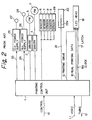
- FIG. 2 is a block diagram of a printer control circuit for use in a conventional non-impact printer.
- a printing control unit 1 transmits, at the time point that a sheet arrives at a printing ready point, a timing signal 12, including a line and a raster timing signal, to a host or another controller, and receives a video signal 11 which has been edited on each page in a host or another controller.
- the received video signal 11 in the printing control unit 1 is transmitted to an LED (Light Emitting Diode) head 19 in the form of a real printing data signal 18.
- the control unit 1 Upon receipt of a line of video signal 11, the control unit 1 transmits a latch of signal 17 to the LED head 19 so as to hold the real printing data signal 18 therein. Before receiving the subsequent data from the other controller, the thus held real printing data signal 18 is visualized in print when the print head 19 receives a printing drive signal 13.
- the real printing data signal 18 is transmitted to the LED head 19 in synchronism with a clock signal 18a.
- FIG. 3 is an operational time chart of the conventional non-impact printer as mentioned above.
- the printing is performed in accordance with image data or video signal 11 transmitted from the host controller as it is, or depending on resolution of the LED head 19 which is determined by an arrangement of the LED devices at regular intervals in a raster direction.
- resolution of the LED head 19 which is determined by an arrangement of the LED devices at regular intervals in a raster direction.
- US-4,437,122 which discloses the features in the preamble of claim 1, describes a method for providing a hard copy output of a video image by storing three successive lines of video data in successive parallelly connected shift registers, applying the outputs of the shift registers to a decoder, and generating driving signals for a printer head.
- the decoder compares the pixels on the same line as well as in preceeding and succeeding lines that surround each specific input pixel to generate the printer head driving signals according to whether straight or curved line segments are to be formed. Thereby the printer increases the density of the information elements and simultaneously provides rounding off of character edges and smoothing of diagonals.
- EP-A-0,132,415 discloses a dot printer for letters or symbols by aggragated dots which generates a second dot matrix pattern from a basic dot matrix pattern by a simple algorithm so that gaps between dots in the basic dot matrix pattern are filled up.
- the basic dot matrix pattern and the second dot matrix pattern are synthetically edited and highgrade printed letters are obtained by using the resulting edited dot matrix pattern.
- a printer according to the present invention is defined in independent claim 1.
- the dependent claims disclose particular embodiments of the invention.
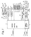
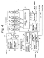
- FIG. 1 a block diagram of a control circuit in a non-impact printer, and FIG. 4, a block diagram of a print data correction circuit included in the embodiment.
- a printing control unit or main control 1 comprises a microprocessor, a ROM, a RAM, input/output ports, a timer and similar components, in the embodiment. and is provided in the inside of a printing unit of a printer.
- the printing control unit 1 provides a sequence control for the printer in its entirety in response to control signals 10 and a video signal 11 from another controller, not shown, such as an interface control unit, a host controller and the like.
- the printing control unit 1 Upon receipt of a print instruction included in the control signals 10, the printing control unit 1 first causes a fuser temperature sensor 29 to sense whether or not a fuser 22 including a heater 22a is in an available temperature range, and if not, turns on the heater 22a timed with signal 21 to heat the fuser 22 up to an available temperature. Next, a motor (PM) 3 for development/transfer process is driven through a driver 2 and simultaneously a high voltage power source 25 for charging is turned on in response to a charge trigger signal 23 to perform charging of a developing unit 27.
- PM motor
- the sort of sheet set is determined on the basis of the results from a sheet remaining amount sensor 8 and a sheet size sensor 9 to start feeding sheets corresponding to the sort of sheet thus sensed.
- a motor 5 for sheet feed is able to rotate in a bilateral direction through a driver 4. The motor 5 first reversely rotates to carry the set sheet by a predetermined amount until a sheet inhalation inlet sensor 6 senses the sheet, and subsequently, regularly rotates to transfer the sheet to a printing device of the inside of the printer.
- the printing control unit 1 transmits, at the time point that the sheet arrives at a printing ready point, a timing signal 12, including a line timing signal and a raster timing signal (receiving clock signal), to the other controller, not shown, and receives a video signal 11.
- a timing signal 12 including a line timing signal and a raster timing signal (receiving clock signal)
- the print data correction circuit 16 will be described in detail, referring to FIG. 4, hereinafter.
- the print data correction circuit 16 comprises a one-line receiving buffer 31, a nine-line buffer 32, selectors 33 and 44, a bilateral buffer 34 having a bilateral selecting function, a receipt address circuit 35, a transmission address circuit 36, a timing signal generation circuit 37 adapted for generating receiving clock signals, transfer clock signals, line timing signals for printing on basic raster lines, and additional line timing signals each for printing on a sub-raster line during an interval of basic raster lines, a logical operation circuit 42, a raster line counter 43 and latch circuits 51-59.
- the video signal 11 which has been edited in units of pages with the resolution of a standard 300 DPI (dot-per-inch) in the other controller or the host controller, is received by the printing control unit 1, and then supplied to the print data correction circuit 16.
- the timing signal generator 37 generates receiving clock signals A and transmits the same to the receipt address circuit 35.
- the entered video signal 11 is stored in storage, locations of the one-line receiving buffer 31, which are addressed by the receipt address circuit 35 whenever the receiving clock signal A is generated. Such storage of the video signal 11 into the one-line receiving buffer 31 is carried out whenever the bilateral buffer 34 receives on a one-line (300 DPI) correspondence basis the video signal 11 from the other controller.
- the video signal 11, which has been stored in the one-line receiving buffer 31, is transferred to the nine-line buffer 32 whenever the reception of a line of video signal 11 is terminated, so that the nine-line buffer 32 stores nine lines of video signal 11.
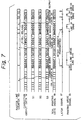
- FIG. 5 shows timings of the printer unit control circuit, in which N denotes the number of line buffers in the print data correction circuit 16.
- N denotes the number of line buffers in the print data correction circuit 16.
- *1 denotes the ⁇ n-6 ⁇ th line of data obtained by a logical operation with data from the ⁇ n-10 ⁇ th line to ⁇ n-2 ⁇ th line with the number of sub-raster lines being 3.
- *2 denotes the (n-5) th line of data obtained by a logical operation with data from the ⁇ n-9 ⁇ th line to the ⁇ n-1 ⁇ th line with the number of sub-raster lines being 3.
- E1, E2,....,E4 denote driving periods of time in the case of printing of a dot on respective basic raster and sub-raster lines 1. 2,...,4.
- the logical operation circuit 42 performs a logical operation on the basis of the video signal 11 stored in the nine-line receiving buffer 32, prior to receipt of the subsequent video signal 11 from the host or the other controller, so as to obtain four real printing data signals 18 as correction output, data.
- the thus obtained four real printing data signals 18 are transferred to an LED head or electrical-to-optical transducer 19 so that a printing is performed with 1,200 DPI pitch in a printing direction.
- the video signal 11 received from the host or another controller is stored in the one-line receiving buffer 31 in synchronism with start-up of the receiving clock signal A.
- An address of the one-line receiving buffer 31 is indicated by the selector 33 which selects an output of the receipt address circuit 35 adapted to stepup in response to trailing down of the receiving clock signals A.
- the bilateral buffer 34 is also selected to send data to line buffer side, so that the data is stored in the one-line receiving buffer 31. This operation is repeated on each entry of data into the one-line receiving buffer 31.
- data transmission processing is performed during a time interval of occurrence of the data receipt timings.
- one indicated by the transmission address selection represents a period of time during which the data transmission processing is performed.
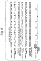
- the timing signal generator 37 generates, as shown in FIG. 6, transfer clock signals B each inhibited only in part of start-up of the receiving clock signal A and having four clocks during a time interval of occurrence of the data receipt timings.
- the transmission address circuit 36 serves to sequentially step up the transmission address in the nine-line buffer 32 in response to the transfer clock signals B.
- nine bits of data in the addressed location which have been stored in storage locations of the same address or "the raster direction dot position" on the continuous, nine lines of video signal stored in the nine-line buffer 32, are read out and transferred through the bilateral buffer 34 to the latch circuit 51.
- the transferred, nine bits of data are latched or held by the latch circuit 51 in timing of start-up of the transfer clock signal B.
- the transmission address circuit 36 serves to sequentially step up the transmission address in the nine-line buffer 32 in accordance with the trailing down of the transfer clock signals B. Accordingly, the corresponding, nine bits of data in the raster direction are transferred to the latch circuit 51 whenever the transfer clock signal B is applied to the transmission address circuit 36.
- the latch circuits 52-59 also latch the entered data in timing of start-up of the transfer clock signals B.
- the respective, nine bits of data of outputs of the latch circuits 51-59 represent data of nine bits or columns in the continuous same raster line direction on the continuous, nine raster lines or rows.
- Both the receipt address circuit 35 and the transmission address circuit 36 serve to repeatedly count the addresses corresponding to the number of dots (now considering 2,560 dots) in the raster direction.
- the timing signal generation circuit 37 transmits transfer clock signal B of which a frequency is five times as high as that of the receiving clock signal A to the transmission address circuit 36.
- the transmission address circuit 36 designates a column address in the raster direction in the nine-line buffer 32
- data of the respective column on the (n-9)th row to the (n-1)th row in the nine-line buffer 32 are read out through the bilateral buffer 34 and latched by the latch circuits 51-59.
- the thus latched data are supplied to the logical operation circuit 42 in the form of the continuous, 9 rows ⁇ 9 columns of data.
- correction output data M in the form of print dot data at a location which becomes a center on a basic raster line correction output data S1 in the form of print dot data on a sub-raster line which locates at a distance of 1/1200 inch from the basic raster line in a printing direction in which printing runs
- correction output data S3 in the form of print dot data on a sub-raster line which locates at a distance of 3/1200 inch from the basic raster line in the printing direction correction output data S3 in the form of print dot data on a sub-raster line which locates at a distance of 3/1200 inch from the basic raster line in the printing direction.
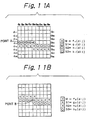
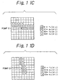
- FIGS. 8A and 8B show in a comparison way dot images formed by the video signal 11 and the correction output data M, S1, S2 and S3, respectively.
- reference numerals 102 and 120 denote the basic raster line and the sub-raster line, respectively.
- a dot at lattice A shown in FIG. 8A produces, in a manner which will be described later, the correction output data S 1 , S 2 and S 3 for forming dots at locations A 1 , A 2 and A 3 placed at a distance of 1/1200 inch downwards from the position of the lattice A in turn.
- the correction output data M has been deleted.
- the correction output data M, S1, S2, and S3 are delayed by a five-column correspondence comparing with the output data from the nine-line buffer 32, since data correction is implemented on the center line of nine lines when nine lines of data are stored in the nine-line buffer 32.
- the real print data signal 18 to be transmitted to the LED head 19 is one selected by the selector 44 among the correction output data M, S1, S2, and S3 by means of counting with an output of the raster line counter 43 the location of the sub-raster lines (1,200 DPI) added between the basic raster lines (300 DPI).
- the correction output data M, S1, S2, and S3 are sequentially transferred to the LED head 19 and then printed.
- the receipt address circuit 35 counts the number of bits, for instance, 2,560 bits in the raster direction
- the'transmission address circuit 36 counts four times the number of bits in the raster direction
- the logical 1 operation circuit 42 performs the logical operation 4 times using nine lines of the same video signal 11.
- a printing in response to the real printing data signal 18 is performed in units of lines, including the sub-raster lines, with 1,200 DPI pitch.
- the real printing data signal 18 is transferred to the LED head 19 in synchronism with the clock signal 18a.
- the latch signal 17 is transmitted whenever the real printing data signal 18 is transmitted the number of bits (2,560 bits) in the raster direction correspondence, so that the transmitted data signal is latched in the LED head 19.
- the LED head 19 is driven in response to the printing drive signal 13 with a predetermined print head drive energy for each line, that is, E1 for the basic raster line, and E2, E3 and E4 for the sub-raster lines.
- the printing control unit 1 includes a drive energy setting circuit S for predetermining the LED head drive energy E1 for printing on the basic raster line and the LED head drive energy E2 for printing on the sub-raster line independently of each other.
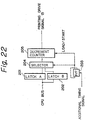
- a block diagram of such a drive energy setting circuit is shown by way of example in FIG. 22.
- digital values which correspond to the LED head drive energy E1 and E2, respectively, are transmitted from a CPU or the like processor unit in the printing control unit 1 on a CPU bus to latches A 201 and B 202, respectively, and then stored therein.
- those latched data are alternately selected by a selector 204 in accordance with an output of a toggle flip-flop 203 which is operative in response to the additional line timing signal, so as to load a decrement counter 205 in response to the additional line timing signal.
- the decrement counter 205 generates a pulse output during a counting period of time.
- This pulse output may be used as the printing drive signal 13.
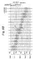
- FIGS. 11A - 11D an operation of the,logical operation circuit 42 will be described.
- respective points A, B, C and D in the 300 DPI array correspond to points A, B and C shown in FIGS. 8A and 8B, and point D shown in FIGS. 10A and 10B, respectively.
- Circles and crosses within the dot matrix on the left denote data to be entered into the logical operation circuit 42.
- Four circles and crosses on the right denote the correction output data M, S1, S2, and S3, respectively.
- the logical operation circuit 42 is provided with a function group ⁇ f n (d ij ) ⁇ for operation of the correction output data M on the basic raster line, and function groups ⁇ g n (d ij ) ⁇ , ⁇ h n (d ij ) ⁇ and ⁇ k n (d ij ) ⁇ for operation of the correction output data S1, S2, and S3 on the sub-raster lines on a parallel basis, so that the the correction output data M, S1, S2, and S3 are simultaneously outputted.
- a result of the operation according to the equations set forth above is a binary value "1"
- a dot is printed, and if "0" , then no dot is printed.
- the results of the operation according to the equations correspond to a position of d 54 of 81 pieces of data, a position located at a distance 1/1200 inch downwards from the position of d 54 , a position located at a distance 2/1200 inch downwards from the position of d 54 , a position located at a distance 3/1200 inch downwards from the position of d 54 , respectively.
- results of the operation according to the function groups f n (d ij ), h n (d ij ) and k n (d ij ) become data representative of position information at A, A 1 , A 2 and A 3 shown in FIG. 8, respectively.
- points B - D similar logical expressions have been prepared.
- Those function groups are defined in such a manner that the correction output data S1, S2, and S3 are determined on each gradient or slope of a line represented by dots of data d 10 to d 98 , and be provided with an arrangement such that the respective functions may be operated on a parallel basis.
- the received video signal 11 of 300 DPI is converted in correction into the real printing data of horizontal 300 DPI and vertical 1,200 DPI, and then transferred to the LED head 19 to be driven.
- FIGS. 9A, 9B, 10A and 10B schematically show in a comparison way printing states according to the conventional non-impact printer and the printer described above. As seen from those figures. it is possible to improve the printing quality in the serrated edge portion, thereby obtaining a smooth slash portion.
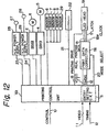
- FIG. 12 a block diagram of a control circuit in a non-impact printer according to an embodiment of the present invention
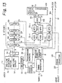
- FIG. 13 a block diagram of a print data correction circuit.
- the control circuit of a non-impact printer shown in FIG. 12 includes a print data correction circuit 116 to which a mode select signal 20 is applied from a printing control unit 101.
- the printing control unit 101 is adapted to generate the mode select signal 20.
- the print data correction circuit 116 shown specifically in FIG. 13 comprises a one-line receiving buffer 31, a nine-line buffer 32, selectors 33 and 44. a bilateral buffer 34 having a bilateral selecting function, a receipt address circuit 35, a transmission address circuit 36, a timing signal generation circuit 37, a mode selector circuit 65, adders 68 and 73-1 to 73-9, a table conversion logical operation circuit 69, and multipliers 75-1 to 75-9.
- the operation of the print data correction circuit 116 is the same as that of the print data correction circuit 16 mentioned above as far as the explanation, up to the point that the data are latched by the latch circuits 51 to 59, is concerned. Consequently, redundant description will be omitted.
- FIG. 14 shows timings of the printer unit control 1 circuit, in which N denotes the number of line buffers in the print data correction circuit 116.
- *1 denotes the ⁇ n-1-(N+1)/2 ⁇ th line of data obtained by a logical operation with data from the ⁇ n-N-1 ⁇ th line to ⁇ n-2 ⁇ th line with the number of additional sub-raster lines being x .
- *2 denotes the ⁇ n-(N+1)/2 ⁇ th line of data obtained by a logical operation with data from the ⁇ n-N ⁇ th line to the ⁇ n-1 ⁇ th line with the number of additional sub-raster lines being x .
- letter A indicates a driving time in the case of printing of a dot on a basic raster line.
- B1, B2,....,Bx denote driving periods of time in the case of printing of a dot on respective sub-raster lines 1, 2, ..., x.
- the multipliers 75-1 to 75-9 the data concerning the obtained location of the center of gravity on each block are multiplied by the weighted correction coefficients each predetermined for the associated block in the mode selector circuit 65 which is operative in response to the mode select signal 20 to output the weighted correction coefficients.
- the respective output values of the multipliers 75-1 to 75-9 are added in the adder 68, thereby obtaining the coordinate (X, Y) of location of the center of gravity as a basis of the correction.
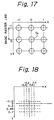
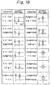
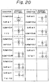
- the coordinate (X, Y) of location of the center of gravity as shown in FIG. 18 is obtained on the basis of a coordinate system as shown in FIG. 17. and the obtained coordinate (X, Y) is converted on the basis of tables as shown in FIGS. 19 and 20 into the output patterns.
- the coordinate (X, Y) of location of the center of gravity is converted into the output pattern comprising dots including a dot, as the center dot, on the basic raster line, and dots on a plurality of sub-raster lines provided between the basic raster lines, and the thus converted output data are transmitted in the respective printing timings, that is, the basic raster timing and the additional raster timing, to the LED head 19 in the form of real printing data signal 18 together with the clock signal 18a.
- the basic raster lines and the sub-raster lines are dots based on the output patterns.
- LED head driving time on the sub-raster lines may be predetermined on each line in the printing control unit 101.
- the LED head driving time may be optionally determined depending on disposition of dots in the output pattern after conversion.
- the printing control 1 unit 101 includes a drive energy setting circuit S for predetermining the LED head drive energy E1 for printing on the basic raster line and the LED head drive energy E2 for printing on the sub-raster line independently of each other.
- a block diagram of such a drive energy setting circuit is shown by way of example in FIG. 22, as described earlier.
- digital values which correspond to the LED head drive energy E1 and E2, respectively, are transmitted from the processor such as a CPU in the printing control unit 1 over the CPU bus to the latches A 201 and B 202, respectively, and then stored therein.
- the latched data are alternately selected by the selector 204 in response to the output from the toggle flip-flop 203 which is operative in response to the additional line timing signal, so as to load the decrement counter 205 in response to the additional line timing signal.
- the decrement counter 205 generates a pulse output during a counting period of time. This pulse output may be used as the printing drive signal 13.
- FIGS. 21A, 21B and 21C schematically showing in a comparison way printing states according to the conventional non-impact printer and the printer of the present invention.
- FIG. 21A shows a dot pattern by the video signal 11, FIG. 21B a dot pattern printed according to the conventional printer, and FIG. 21C a dot pattern printed according to the printer of the present invention.
Landscapes
- Physics & Mathematics (AREA)
- Engineering & Computer Science (AREA)
- Optics & Photonics (AREA)
- General Engineering & Computer Science (AREA)
- General Physics & Mathematics (AREA)
- Theoretical Computer Science (AREA)
- Printers Or Recording Devices Using Electromagnetic And Radiation Means (AREA)
- Fax Reproducing Arrangements (AREA)
- Exposure Or Original Feeding In Electrophotography (AREA)
- Accessory Devices And Overall Control Thereof (AREA)
- Dot-Matrix Printers And Others (AREA)
Applications Claiming Priority (4)
| Application Number | Priority Date | Filing Date | Title |
|---|---|---|---|
| JP16587391 | 1991-07-05 | ||
| JP165873/91 | 1991-07-05 | ||
| JP16587391A JP2804187B2 (ja) | 1991-07-05 | 1991-07-05 | ノンインパクトプリンタ |
| EP92111126A EP0526738B1 (en) | 1991-07-05 | 1992-07-01 | Printer having print data correction circuit |
Related Parent Applications (2)
| Application Number | Title | Priority Date | Filing Date |
|---|---|---|---|
| EP92111126A Division EP0526738B1 (en) | 1991-07-05 | 1992-07-01 | Printer having print data correction circuit |
| EP92111126.6 Division | 1992-07-01 |
Publications (3)
| Publication Number | Publication Date |
|---|---|
| EP0744707A2 EP0744707A2 (en) | 1996-11-27 |
| EP0744707A3 EP0744707A3 (en) | 1997-10-01 |
| EP0744707B1 true EP0744707B1 (en) | 2001-11-14 |
Family
ID=15820607
Family Applications (2)
| Application Number | Title | Priority Date | Filing Date |
|---|---|---|---|
| EP92111126A Expired - Lifetime EP0526738B1 (en) | 1991-07-05 | 1992-07-01 | Printer having print data correction circuit |
| EP96112045A Expired - Lifetime EP0744707B1 (en) | 1991-07-05 | 1992-07-01 | Printer having print data correction circuit |
Family Applications Before (1)
| Application Number | Title | Priority Date | Filing Date |
|---|---|---|---|
| EP92111126A Expired - Lifetime EP0526738B1 (en) | 1991-07-05 | 1992-07-01 | Printer having print data correction circuit |
Country Status (4)
| Country | Link |
|---|---|
| US (2) | US6373513B1 (ja) |
| EP (2) | EP0526738B1 (ja) |
| JP (1) | JP2804187B2 (ja) |
| DE (2) | DE69227418T2 (ja) |
Families Citing this family (13)
| Publication number | Priority date | Publication date | Assignee | Title |
|---|---|---|---|---|
| JP2866758B2 (ja) * | 1991-07-05 | 1999-03-08 | 沖電気工業株式会社 | ノンインパクトプリンタ |
| JP3319023B2 (ja) * | 1993-04-15 | 2002-08-26 | カシオ電子工業株式会社 | 記録装置 |
| JP2616697B2 (ja) * | 1994-06-06 | 1997-06-04 | 日本電気株式会社 | 印字画素制御回路 |
| DE19506792C2 (de) * | 1995-02-27 | 2001-05-03 | Oce Printing Systems Gmbh | Verfahren und Vorrichtung zur Steigerung der Bildqualität in Bildausgabegeräten |
| DE19506791C1 (de) * | 1995-02-27 | 1996-02-15 | Siemens Nixdorf Inf Syst | Vorrichtung zur Steigerung der Druckqualität in Hochgeschwindigkeitsdruck- und -kopiergeräten |
| NL1002975C2 (nl) * | 1996-05-01 | 1997-11-06 | Oce Tech Bv | Werkwijze en inrichting voor het verbeterd afdrukken van digitale halftoonbeelden. |
| JP2856149B2 (ja) * | 1996-05-15 | 1999-02-10 | 日本電気株式会社 | 電子写真プリンタ |
| JPH106559A (ja) * | 1996-06-26 | 1998-01-13 | Nec Niigata Ltd | Ledプリンタ |
| JP3079076B2 (ja) * | 1997-03-19 | 2000-08-21 | 富士通株式会社 | 画像形成装置 |
| WO2002019694A1 (fr) * | 2000-08-31 | 2002-03-07 | Ricoh Company, Limited | Dispositif imageur |
| JP4270781B2 (ja) | 2000-11-02 | 2009-06-03 | 株式会社沖データ | 画像記録方法及び装置 |
| US6476845B2 (en) | 2000-12-13 | 2002-11-05 | Hewlett-Packard Co. | Electrophotographic printer, and method of controlling light emitting elements in an electrophotographic print head |
| US8964245B2 (en) | 2010-08-31 | 2015-02-24 | Hewlett-Packard Development Company, L.P. | Color plane registration error measurement |
Family Cites Families (18)
| Publication number | Priority date | Publication date | Assignee | Title |
|---|---|---|---|---|
| JPS56109068A (en) * | 1980-02-04 | 1981-08-29 | Nippon Telegr & Teleph Corp <Ntt> | Recorder for multitone |
| US4398256A (en) * | 1981-03-16 | 1983-08-09 | Hughes Aircraft Company | Image processing architecture |
| US4437122A (en) * | 1981-09-12 | 1984-03-13 | Xerox Corporation | Low resolution raster images |
| DE3474933D1 (en) * | 1983-07-26 | 1988-12-08 | Oki Electric Ind Co Ltd | Printing system for a dot printer |
| JPS60165864A (ja) * | 1984-02-09 | 1985-08-29 | Yokogawa Hokushin Electric Corp | レ−ザプリンタ |
| US4703323A (en) * | 1985-01-29 | 1987-10-27 | International Business Machines Corporation | Method and apparatus for displaying enhanced dot matrix characters |
| JPS6240872A (ja) * | 1985-08-16 | 1987-02-21 | Seikosha Co Ltd | 感熱記録装置 |
| JPS63146061A (ja) * | 1986-12-10 | 1988-06-18 | Ricoh Co Ltd | 記録装置 |
| US4837587A (en) * | 1987-12-31 | 1989-06-06 | Eastman Kodak Company | Non-impact printer with nonuniformity correction |
| JPH0260768A (ja) * | 1988-08-26 | 1990-03-01 | Canon Inc | 記録装置 |
| JPH0259362A (ja) * | 1988-08-25 | 1990-02-28 | Canon Inc | 記録装置 |
| JPH02162475A (ja) * | 1988-12-15 | 1990-06-22 | Dainippon Screen Mfg Co Ltd | 画像輪郭修正方法 |
| EP0416886B1 (en) * | 1989-09-06 | 1995-04-19 | Canon Kabushiki Kaisha | Image recording apparatus |
| US5025322A (en) | 1989-12-18 | 1991-06-18 | Eastman Kodak Company | Method and apparatus for grey level recording using multiple addressability |
| US5130821A (en) * | 1990-04-16 | 1992-07-14 | Eastman Kodak Company | Method and apparatus for digital halftoning employing density distribution for selection of a threshold template |
| JP2866752B2 (ja) * | 1991-02-12 | 1999-03-08 | 沖電気工業株式会社 | ノンインパクトプリンタ |
| US5134495A (en) * | 1990-11-07 | 1992-07-28 | Dp-Tek, Inc. | Resolution transforming raster-based imaging system |
| US5193008A (en) | 1990-11-07 | 1993-03-09 | Dp-Tek, Inc. | Interleaving vertical pixels in raster-based laser printers |
-
1991
- 1991-07-05 JP JP16587391A patent/JP2804187B2/ja not_active Expired - Lifetime
-
1992
- 1992-07-01 EP EP92111126A patent/EP0526738B1/en not_active Expired - Lifetime
- 1992-07-01 DE DE69227418T patent/DE69227418T2/de not_active Expired - Lifetime
- 1992-07-01 DE DE69232209T patent/DE69232209T2/de not_active Expired - Lifetime
- 1992-07-01 EP EP96112045A patent/EP0744707B1/en not_active Expired - Lifetime
-
1995
- 1995-04-26 US US08/427,812 patent/US6373513B1/en not_active Expired - Fee Related
- 1995-04-26 US US08/427,823 patent/US6049349A/en not_active Expired - Lifetime
Also Published As
| Publication number | Publication date |
|---|---|
| DE69227418T2 (de) | 1999-05-06 |
| DE69227418D1 (de) | 1998-12-03 |
| US6049349A (en) | 2000-04-11 |
| DE69232209T2 (de) | 2002-06-27 |
| US6373513B1 (en) | 2002-04-16 |
| JPH058438A (ja) | 1993-01-19 |
| EP0744707A2 (en) | 1996-11-27 |
| EP0744707A3 (en) | 1997-10-01 |
| EP0526738A3 (en) | 1993-08-11 |
| DE69232209D1 (de) | 2001-12-20 |
| EP0526738B1 (en) | 1998-10-28 |
| JP2804187B2 (ja) | 1998-09-24 |
| EP0526738A2 (en) | 1993-02-10 |
Similar Documents
| Publication | Publication Date | Title |
|---|---|---|
| EP0521491B1 (en) | Printer having circuit for providing improved printing quality | |
| EP0526738B1 (en) | Printer having print data correction circuit | |
| US5384646A (en) | Marking engine for grey level printing having a high productivity image data processing mode | |
| GB2119982A (en) | Printer | |
| US6016154A (en) | Image forming apparatus | |
| US5742317A (en) | Image processing apparatus and recording apparatus | |
| EP0769756A2 (en) | Image forming apparatus | |
| EP0476863B1 (en) | Method and printer for printing an image formed of 2-dimensionally arranged pixels | |
| JP3856361B2 (ja) | 画像データ処理方法および装置 | |
| EP0484919B1 (en) | Printer having print data arithmetic logic | |
| US5539525A (en) | Image printing method and non-impact printer wherein a received video signal has a higher resolution than the printer printing head | |
| JP3990086B2 (ja) | 画像データ処理装置 | |
| EP0620535B1 (en) | Line printer for high density printing | |
| JP2004351932A (ja) | タンデムプリンタ用の画像データを効率的に生成し、供給するシステム及び方法 | |
| US8098252B2 (en) | Parallel video processing architecture | |
| JP2002158877A (ja) | 画像データ処理方法及び画像データ処理装置 | |
| JP3552263B2 (ja) | 画像データ処理装置 | |
| JP2002057885A (ja) | 画像処理装置と画像処理方法 | |
| JPH0531958A (ja) | 画像形成装置 | |
| JP2002209091A (ja) | ある解像度からより低い解像度に画像を変換する方法 | |
| HK1013480B (en) | Line printer for high density printing | |
| JPH0823873B2 (ja) | 画像形成装置 | |
| JP2000069283A (ja) | 画像データ処理装置 | |
| JPH1032717A (ja) | 画像データ処理装置 | |
| JPH10151816A (ja) | 画像記録装置 |
Legal Events
| Date | Code | Title | Description |
|---|---|---|---|
| PUAI | Public reference made under article 153(3) epc to a published international application that has entered the european phase |
Free format text: ORIGINAL CODE: 0009012 |
|
| AC | Divisional application: reference to earlier application |
Ref document number: 526738 Country of ref document: EP |
|
| AK | Designated contracting states |
Kind code of ref document: A2 Designated state(s): DE FR GB |
|
| PUAL | Search report despatched |
Free format text: ORIGINAL CODE: 0009013 |
|
| AK | Designated contracting states |
Kind code of ref document: A3 Designated state(s): DE FR GB |
|
| 17P | Request for examination filed |
Effective date: 19980105 |
|
| 17Q | First examination report despatched |
Effective date: 19990903 |
|
| RAP1 | Party data changed (applicant data changed or rights of an application transferred) |
Owner name: OKI DATA CORPORATION |
|
| GRAG | Despatch of communication of intention to grant |
Free format text: ORIGINAL CODE: EPIDOS AGRA |
|
| GRAG | Despatch of communication of intention to grant |
Free format text: ORIGINAL CODE: EPIDOS AGRA |
|
| GRAH | Despatch of communication of intention to grant a patent |
Free format text: ORIGINAL CODE: EPIDOS IGRA |
|
| GRAH | Despatch of communication of intention to grant a patent |
Free format text: ORIGINAL CODE: EPIDOS IGRA |
|
| GRAA | (expected) grant |
Free format text: ORIGINAL CODE: 0009210 |
|
| AC | Divisional application: reference to earlier application |
Ref document number: 526738 Country of ref document: EP |
|
| AK | Designated contracting states |
Kind code of ref document: B1 Designated state(s): DE FR GB |
|
| REF | Corresponds to: |
Ref document number: 69232209 Country of ref document: DE Date of ref document: 20011220 |
|
| REG | Reference to a national code |
Ref country code: GB Ref legal event code: IF02 |
|
| ET | Fr: translation filed | ||
| PLBE | No opposition filed within time limit |
Free format text: ORIGINAL CODE: 0009261 |
|
| STAA | Information on the status of an ep patent application or granted ep patent |
Free format text: STATUS: NO OPPOSITION FILED WITHIN TIME LIMIT |
|
| 26N | No opposition filed | ||
| PGFP | Annual fee paid to national office [announced via postgrant information from national office to epo] |
Ref country code: GB Payment date: 20110629 Year of fee payment: 20 |
|
| PGFP | Annual fee paid to national office [announced via postgrant information from national office to epo] |
Ref country code: FR Payment date: 20110727 Year of fee payment: 20 |
|
| PGFP | Annual fee paid to national office [announced via postgrant information from national office to epo] |
Ref country code: DE Payment date: 20110629 Year of fee payment: 20 |
|
| REG | Reference to a national code |
Ref country code: DE Ref legal event code: R071 Ref document number: 69232209 Country of ref document: DE |
|
| REG | Reference to a national code |
Ref country code: DE Ref legal event code: R071 Ref document number: 69232209 Country of ref document: DE |
|
| REG | Reference to a national code |
Ref country code: GB Ref legal event code: PE20 Expiry date: 20120630 |
|
| PG25 | Lapsed in a contracting state [announced via postgrant information from national office to epo] |
Ref country code: GB Free format text: LAPSE BECAUSE OF EXPIRATION OF PROTECTION Effective date: 20120630 |
|
| PG25 | Lapsed in a contracting state [announced via postgrant information from national office to epo] |
Ref country code: DE Free format text: LAPSE BECAUSE OF EXPIRATION OF PROTECTION Effective date: 20120703 |