EP0744817A2 - Transfert inverse d'énergie dans un convertisseur de puissance à commutation par courant nul - Google Patents
Transfert inverse d'énergie dans un convertisseur de puissance à commutation par courant nul Download PDFInfo
- Publication number
- EP0744817A2 EP0744817A2 EP96303034A EP96303034A EP0744817A2 EP 0744817 A2 EP0744817 A2 EP 0744817A2 EP 96303034 A EP96303034 A EP 96303034A EP 96303034 A EP96303034 A EP 96303034A EP 0744817 A2 EP0744817 A2 EP 0744817A2
- Authority
- EP
- European Patent Office
- Prior art keywords
- converter
- switch
- inductor
- input source
- current
- Prior art date
- Legal status (The legal status is an assumption and is not a legal conclusion. Google has not performed a legal analysis and makes no representation as to the accuracy of the status listed.)
- Granted
Links
Images


Classifications
-
- H—ELECTRICITY
- H02—GENERATION; CONVERSION OR DISTRIBUTION OF ELECTRIC POWER
- H02M—APPARATUS FOR CONVERSION BETWEEN AC AND AC, BETWEEN AC AND DC, OR BETWEEN DC AND DC, AND FOR USE WITH MAINS OR SIMILAR POWER SUPPLY SYSTEMS; CONVERSION OF DC OR AC INPUT POWER INTO SURGE OUTPUT POWER; CONTROL OR REGULATION THEREOF
- H02M3/00—Conversion of DC power input into DC power output
- H02M3/22—Conversion of DC power input into DC power output with intermediate conversion into AC
- H02M3/24—Conversion of DC power input into DC power output with intermediate conversion into AC by static converters
- H02M3/28—Conversion of DC power input into DC power output with intermediate conversion into AC by static converters using discharge tubes with control electrode or semiconductor devices with control electrode to produce the intermediate AC
- H02M3/325—Conversion of DC power input into DC power output with intermediate conversion into AC by static converters using discharge tubes with control electrode or semiconductor devices with control electrode to produce the intermediate AC using devices of a triode or a transistor type requiring continuous application of a control signal
- H02M3/335—Conversion of DC power input into DC power output with intermediate conversion into AC by static converters using discharge tubes with control electrode or semiconductor devices with control electrode to produce the intermediate AC using devices of a triode or a transistor type requiring continuous application of a control signal using semiconductor devices only
- H02M3/33569—Conversion of DC power input into DC power output with intermediate conversion into AC by static converters using discharge tubes with control electrode or semiconductor devices with control electrode to produce the intermediate AC using devices of a triode or a transistor type requiring continuous application of a control signal using semiconductor devices only having several active switching elements
- H02M3/33576—Conversion of DC power input into DC power output with intermediate conversion into AC by static converters using discharge tubes with control electrode or semiconductor devices with control electrode to produce the intermediate AC using devices of a triode or a transistor type requiring continuous application of a control signal using semiconductor devices only having several active switching elements having at least one active switching element at the secondary side of an isolation transformer
-
- H—ELECTRICITY
- H02—GENERATION; CONVERSION OR DISTRIBUTION OF ELECTRIC POWER
- H02M—APPARATUS FOR CONVERSION BETWEEN AC AND AC, BETWEEN AC AND DC, OR BETWEEN DC AND DC, AND FOR USE WITH MAINS OR SIMILAR POWER SUPPLY SYSTEMS; CONVERSION OF DC OR AC INPUT POWER INTO SURGE OUTPUT POWER; CONTROL OR REGULATION THEREOF
- H02M3/00—Conversion of DC power input into DC power output
- H02M3/02—Conversion of DC power input into DC power output without intermediate conversion into AC
- H02M3/04—Conversion of DC power input into DC power output without intermediate conversion into AC by static converters
- H02M3/10—Conversion of DC power input into DC power output without intermediate conversion into AC by static converters using discharge tubes with control electrode or semiconductor devices with control electrode
- H02M3/145—Conversion of DC power input into DC power output without intermediate conversion into AC by static converters using discharge tubes with control electrode or semiconductor devices with control electrode using devices of a triode or transistor type requiring continuous application of a control signal
- H02M3/155—Conversion of DC power input into DC power output without intermediate conversion into AC by static converters using discharge tubes with control electrode or semiconductor devices with control electrode using devices of a triode or transistor type requiring continuous application of a control signal using semiconductor devices only
- H02M3/156—Conversion of DC power input into DC power output without intermediate conversion into AC by static converters using discharge tubes with control electrode or semiconductor devices with control electrode using devices of a triode or transistor type requiring continuous application of a control signal using semiconductor devices only with automatic control of output voltage or current, e.g. switching regulators
- H02M3/158—Conversion of DC power input into DC power output without intermediate conversion into AC by static converters using discharge tubes with control electrode or semiconductor devices with control electrode using devices of a triode or transistor type requiring continuous application of a control signal using semiconductor devices only with automatic control of output voltage or current, e.g. switching regulators including plural semiconductor devices as final control devices for a single load
-
- H—ELECTRICITY
- H02—GENERATION; CONVERSION OR DISTRIBUTION OF ELECTRIC POWER
- H02M—APPARATUS FOR CONVERSION BETWEEN AC AND AC, BETWEEN AC AND DC, OR BETWEEN DC AND DC, AND FOR USE WITH MAINS OR SIMILAR POWER SUPPLY SYSTEMS; CONVERSION OF DC OR AC INPUT POWER INTO SURGE OUTPUT POWER; CONTROL OR REGULATION THEREOF
- H02M7/00—Conversion of AC power input into DC power output; Conversion of DC power input into AC power output
- H02M7/02—Conversion of AC power input into DC power output without possibility of reversal
- H02M7/04—Conversion of AC power input into DC power output without possibility of reversal by static converters
- H02M7/12—Conversion of AC power input into DC power output without possibility of reversal by static converters using discharge tubes with control electrode or semiconductor devices with control electrode
- H02M7/21—Conversion of AC power input into DC power output without possibility of reversal by static converters using discharge tubes with control electrode or semiconductor devices with control electrode using devices of a triode or transistor type requiring continuous application of a control signal
- H02M7/217—Conversion of AC power input into DC power output without possibility of reversal by static converters using discharge tubes with control electrode or semiconductor devices with control electrode using devices of a triode or transistor type requiring continuous application of a control signal using semiconductor devices only
Definitions
- This invention relates to zero-current switching power conversion.
- Fig. 1 shows a circuit schematic of an idealized non-isolated ZCS buck converter 10.
- the converter may be operated in either a half-wave or a full-wave mode of operation.
- the switch 25 is closed by the ZCS switch controller 12 at a time of zero flow of current Iin.
- the switch 25 is opened by the ZCS switch controller 12 on the occurrence of the first zero crossing of current following switch closure.
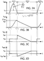
- Waveforms for the half-wave mode are shown in Figures 3A through 3D.
- the switch 25 is opened by the ZCS switch controller 12 on the occurrence of the second (or any even numbered) zero crossing following switch closure.
- Waveforms for the full-wave mode are shown in Figure 4A through 4D.
- An output filter 16 in the converter 10 filters the pulsating voltage Vc(t) to deliver an essentially DC output voltage, Vout, across the load.
- a frequency controller 15 compares the converter output voltage, Vout, to a reference value (indicative of some desired value of Vout, but not shown) and sets the converter operating frequency, fop, to a value consistent with maintaining Vout at the desired value.
- a ZCS converter will exhibit higher conversion efficiency than a conventional pulse-width modulated ("PWM") buck converter (20, Figure 2) because opening and closing the switch 25 at essentially zero current results in a substantial reduction in switching losses.
- PWM pulse-width modulated
- the reduction in switching losses allows for an increase in converter operating frequency and a corresponding decrease in the size of a ZCS converter relative to its PWM counterpart.
- half-wave mode In half-wave mode, a finite and bounded amount of energy is withdrawn by the converter from the input source 14 during each converter operating cycle (the "half-wave" energy) and all of this energy is delivered to the load during the cycle. As a result, maintaining a constant load voltage requires that converter operating frequency be varied essentially in proportion to the converter load. If the converter is operated in full-wave mode, the first half of the operating cycle is identical to the half-wave operating mode and an amount of energy equal to the half-wave energy is withdrawn from the input source 14. However, during the second half of the operating cycle (between the first and second zero crossings) a portion of this energy is returned to the input source 14 with the remainder being delivered to the load.
- the ratio of the amount of the energy which is returned to the source 14 to the amount of the energy which is provided to the load varies with converter loading; as a result, converter operating frequency tends to be relatively constant and independent of load.
- the half-wave ZCS converter is a "quantized" converter in the sense that a predictable amount of energy is delivered to the load during each converter operating cycle. This is in contrast to the full-wave ZCS converter in which a variable fraction of the total half-wave energy extracted from the input source is actually delivered to the load during each operating cycle.
- half-wave ZCS converters operating in synchronism will accurately share in the power delivered to a load; practical embodiments of full-wave converters will not.
- the relatively constant, high, operating frequency of the full-wave mode mitigates toward both a smaller converter (e.g., the breakpoint frequency of the converter output filter may be raised, thereby reducing the size of the filter components) and improved converter performance (e.g., the higher output filter breakpoint frequency will allow wider overall converter bandwidth and a concomitant improvement in transient response).
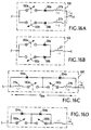
- FIG. 3A shows a ZCS buck converter 30 using a MOSFET transistor 26 as the switching element.
- Such a device is not capable of supporting a bipolar voltage due to the "intrinsic" diode 31 inherent to the MOSFET.
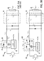
- a ZCS converter 30, adapted to operate in half cycle mode and shown in Figure 5B, includes a composite switch 125, comprising a diode 38 in series with a MOSFET switch 26, capable of blocking negative values of Vsw. The losses attendant to the flow of current Iin in this diode results in a reduction in conversion efficiency.
- a bipolar switch in a ZCS converter: in a half-wave converter a series diode (38, Fig. 6A) will generally be needed to form a composite switch 25a capable of blocking negative values of Vsw; in a full-wave converter an anti-parallel diode (34, Fig. 6B) is required to conduct negative flow of Iin.
- the references illustrate the use of diodes in series or in parallel with MOSFET and bipolar switches to adapt the switches to half-wave or full-wave operation and also discuss the concept of the "resonant switch" as applied to ZCS conversion.
- the resonant switch concept provides for replacing a switching element in a PWM converter topology with a resonant switch comprising a switching element, a capacitor, an inductor and one or more diodes (depending on whether the application is a half-wave or full-wave) to create a corresponding ZCS topology.
- Saturable inductors are well known. They typically consist of a winding on a magnetic core having a known value of saturation flux density (where the "saturation flux density” is the value of flux density below which the permeability of the core is relatively high and above which the value of the permeability of the core is relatively low), exhibit a relatively high value of inductance at relatively low values of current (e.g. values which do not cause the flux density in the core to exceed the saturation flux density) and a relatively much lower value of inductance at relatively higher currents (e.g. values which would otherwise cause the flux density in the core to exceed the saturation flux density).
- saturation flux density is the value of flux density below which the permeability of the core is relatively high and above which the value of the permeability of the core is relatively low
- the flux in the core which links the winding will be proportional to the time integral of the voltage across the winding (i.e. the "volt-seconds" applied to the device). If the applied "volt-seconds" exceeds a certain value (dependent upon the number of turns in the winding and the dimensions and saturation flux density of the core) the magnetic flux linking the core will exceed the saturation flux density and the inductance of the device will drop.
- a saturable inductor to modify the shape of the current and voltage waveforms in both half-wave and full-wave ZCS converters, of both the buck and boost types, is described in Erikson, "Nonlinear Resonant Switch and Converter," U. S. Patent No. 4,829,232, May 9, 1989.
- the saturable inductor is used in place of a fixed resonant inductor (e.g., inductor 27, Figure 1) and arranged to saturate and assume a low inductance value at low values of current and to unsaturate and assume a high inductance value at high currents.
- One way to achieve this would be to place a diode in series with the switch 39; another way, described in that application, is to connect a saturable inductor 37, having a volt-second capability sufficiently large to support the voltage Vc(t) throughout the time that the voltage is negative (e.g., between times ta and tb) subsequent to the switch being opened, in series with the switch 39.
- a general class of ZCS boost converters using coupled inductors, and semiconductor switch topologies for use in both half-wave and full-wave versions of the converters are described in Vinciarelli, et al, "Boost Switching Power Conversion," U. S. Patent No. 5,321,348, June 14, 1994 (incorporated by reference).
- ZCS boost converters which deliver a DC output but which are operated directly from an AC (e.g., bipolar) input source are described in our European Patent Application No. 95304870.9 (published as EP-A-0692863) (incorporated by reference).
- the invention features a zero-current switching converter for converting power from an input source for delivery to a load.
- a switch opens and closes at times of essentially zero current to enable energy transfer back and forth between said input source and said converter.
- a controller is connected to control the switch to initiate, during a first portion of each of a succession of converter operating cycles, forward energy transfer from said input source; and in at least some of said converter operating cycles, also to initiate reverse energy transfer to said input source at times not contiguous with said first portion.
- the forward energy transfer may be initiated by closing the switch.
- the reverse energy transfer may also be initiated by closing said switch.
- the initiation of reverse energy transfer may occur a predetermined time after the beginning of the first portion.
- the minimum frequency of the converter operating cycles may be controlled by controlling a time delay between the beginning of the first portion and the initiation of the reverse energy transfer.
- circuit elements e.g., an inductor and a capacitor
- There may be a saturable inductor and the time between the beginning of the first portion and the initiation of reverse energy transfer may be determined by the volt-second characteristic of the saturable inductor.
- the switch may include two switching elements each connected to transfer energy between the input source and the converter.
- a first switching element connected in series with a first (e.g., saturable) inductor, may set a characteristic time constant associated transfer of energy from the input source.
- a second switching element connected in series with a second (e.g., saturable) inductor, may set a characteristic time constant associated with the transfer of energy toward the input source.
- a saturable inductor may be connected to carry the current (currents) which flows in the switching element (elements).
- the zero-current switching converter may be a buck converter, a boost converter, and AC-DC boost converter, a buck-boost converter, a Cuk converter a SEPIC converter, a non-isolated converter, or an isolated converter, among others.
- the input source may include a unipolar voltage.
- the switch may be connected in series with the input source and the first inductor.
- There may be an output filter connected between the capacitor and the load for delivering energy from the capacitor to the load at an average voltage essentially equal to the average voltage across the capacitor.
- a diode may be connected in parallel with the capacitor and poled to block a voltage of the polarity of the average voltage.
- An input inductor may be connected in series with the input source and the series circuit, and a diode may be connected between the capacitor and the load, the diode poled to conduct current in a direction to deliver energy from the input source to the load.
- the switching element may be a unidirectional switch poled to block the voltage delivered by the input source when the switching element is open.
- the saturable inductor may be arranged to exhibit a relatively high unsaturated impedance during portions of the operating cycle during which reverse voltage would otherwise have to be blocked by the switching element.
- the input source may be a bipolar voltage source, the capacitor may be connected in parallel with the series circuit comprising the switch and the first inductor, an input inductor may be connected in series with the input source and the series circuit, and a rectifier may be connected between the dual-mode switch and the load, the rectifier accepting a bipolar input current and delivering a unipolar output current to the load.
- the inductance may be the leakage inductance of a leakage-inductance transformer comprising a primary winding and a secondary winding.
- the first switching element may be connected in series with the primary winding.
- a second switching element may be connected in series with both the secondary winding and the capacitor, the first switching element and the primary winding being connected in series with the input source.
- An output filter may be connected between the capacitor and the load for delivering energy from the capacitor to the load at an average voltage essentially equal to the average voltage across the capacitor.
- a diode may be connected in parallel with the capacitor and poled to block a voltage of the polarity of the average voltage.
- the reverse energy transfer may be initiated if the voltage across the capacitor is greater than the voltage delivered by the input source.
- the reverse energy transfer may be initiated if the voltage across the capacitor is at a value such that the absolute value of the incremental change in the capacitor voltage which must occur to enable current to flow into the load is greater than the voltage across the load.
- the invention features a method of controlling the minimum operating frequency of a zero-current switching converter which transfers power from an input source for delivery to a time-varying load by opening and closing a switch at times of zero current flow.
- the switch In a first portion of each of a series of converter operating cycles, the switch is controlled to initiate forward energy transfer from the input source.
- controlling the switch In response to changes of the load, during each of some of the converter operating cycles and at times which are not contiguous with the first portion, controlling the switch to initiate reverse energy transfer to the input source.
- Implementations of the invention may include one or more of the following features.
- a fixed time delay may be caused between the beginning of the first portion and the initiation of the reverse energy transfer.
- the time delay between the beginning of the first portion and the initiation of the reverse energy transfer may be selectively adjusted.
- the volt-second characteristic of a saturable inductor may be adapted to effect a controlled time delay between the beginning of the first portion and the initiation of the reverse energy transfer.
- the reverse energy transfer may be initiated if doing so will result in energy being transferred from the converter back to the input source.
- the reverse energy transfer may be initiated on the basis of a voltage measured across a capacitor.
- the output filter breakpoint frequency may be raised which mitigates toward smaller, less lossy, filter components and wider converter bandwidth; conducted and radiated EMI/RFI filters and shields become smaller; and the potential for frequency-specific interference within load circuitry can be eliminated.
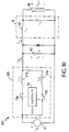
- FIG. 10 A circuit model which demonstrates the operating principle of a ZCS converter topology which provides for setting a lower limit on converter operating frequency while retaining the benefits of half-wave operation (e.g., efficiency, power sharing) at elevated loads, is illustrated in Figure 10.
- a ZCS buck converter 100 includes the same circuit elements as the prior art ZCS buck converter of Figure 1, except that the switch 25 and the resonant inductor 27 of Figure 1 are replaced with a "multi-mode switch" 105 in the converter of Figure 10.
- the multi-mode switch consists of a first switching element 75a in series with a first resonant inductor 27a, of value Lr1, and a second switching element 75b in series with a second resonant inductor 27b, of value Lr2.
- the multi-mode switch 105 also includes a dual-mode switch controller 112, a simplified functional schematic of which is shown in Figure 11A.
- the first ZCS switch controller 12a opens and closes the first switch 75a at zero current to initiate a forward flow of current, Iin (Fig. 12C), and forward transfer of energy from the input source 14 toward the capacitor 42 via the first inductor 27a.
- This initial part of the operating cycle is seen to be essentially identical to the initial portion of an operating cycle in the prior art ZCS buck converter operating in half-wave mode (e.g., as shown in Figure 3). However, if a new trigger signal is not received within a predetermined delay time, Td, after the initiation of forward energy transfer (where Td ends after the forward energy transfer phase has ended, e.g.
- the second ZCS switch controller 12b will be triggered by the output of delay element 17 causing switch 75b to open and close at zero current, and resulting in a reverse flow of current, Iin, and a reverse flow of energy from the capacitor 42 back to the input source 14 via inductor 27b (provided that the capacitor voltage, Vc(Td) is greater than the input voltage, Vin, at time Td; if the voltage Vc(Td) is below Vin, the second switch will not be activated).
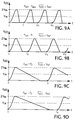
- the waveforms of Figure 9 illustrate that a significant reduction in operating frequency is required in a prior art ZCS converter operating in the half-wave operating mode to maintain a constant output voltage as load drops. If, however, as illustrated in Figures 13A through 13D, the half-wave cycle is aborted at time Td and energy stored in the capacitor 42 is returned back to the input source, then the variation in operating frequency can be substantially reduced.
- the waveform in Figure 9A is the same as that in Figure 13A and the waveforms in Figures 9B and 13B are also the same, because, in both cases, Vc is below Vin at time Td; reverse energy transfer will not occur for Vc ⁇ Vin and is therefore not initiated.
- the efficiency and power sharing benefits of the half-wave converter can be provided at relatively high values of load, where they are of the most benefit.
- initiation of reverse energy transfer puts a lower bound on converter operating frequency and provides for the previously described benefits.
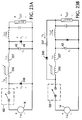
- FIG. 11B A more detailed schematic of a dual-mode controller 112, of the kind shown in Figure 11A, is shown in Figure 11B.
- trigger signals 77 arriving at the operating frequency fop are delivered both to first ZCS switch controller 12A and to retriggerable monostable 117.
- the first ZCS controller initiates forward half-wave flow of current Iin.
- the retriggerable monostable 117 generates a logically high output for a time period equal to Td (and, if fop exceeds 1/Td, the output of the monostable will stay in a logically high state).
- Inverter 72 and AND gate 74 combine the output of the monostable 117 with the output of comparator 70 (a signal indicative of whether the capacitor voltage Vc is greater than the converter input voltage Vin). If the time period Td has elapsed and Vc > Vin, then the second monostable 76 will be triggered to produce a brief pulse for activating the second ZCS controller 126 and initiating a reverse energy transfer phase. If Vc ⁇ Vin at time Td, or if fop > 1/Td, the second ZCS controller will not be activated.
- the converter 100 and multi-mode switch 105 of Figures 10 and 11 provide for two distinct characteristic time constants for the forward and reverse energy transfer phases. In many applications this will not be a requirement and the multi-mode switch 105 may be simplified to the form shown in Figure 14.
- the multi-mode switch 105 uses a single inductor 27 to provide a single characteristic time constant for both the forward and reverse energy transfer phases, and a dual-mode controller 112 for opening and closing the single ideal switch 75 (which is able to block a bipolar voltage when open and carry a bipolar current when closed) at the same times that the dual-mode controller 112 opened the two ideal switches 75a, 75b of Figure 11.
- the generalized unidirectional switch 130 of Figure 15A is capable of blocking a voltage Vsw having the polarity indicated in the Figure and is therefore symbolic of the N-channel MOSFET 61 poled as shown in Figure 15B and the P-channel MOSFET 62 poled as shown in Figure 15C. It is also symbolic of the NPN transistor 63 poled as shown in Figure 15D and the PNP transistor 64 poled as shown in Figure 15C.
- the bipolar transistors 63, 64 can typically support a low value of reverse voltage (e.g., negative values of Vsw up to about 6.5 volts, which is typical of the reverse avalanche breakdown voltage rating of the base-emitter junction of a bipolar transistor).
- the bipolar devices may be considered to be unidirectional switches.
- FIGs 16A through 16D show embodiments of multi-mode switches 105 which comprise unidirectional switches 105 (using the symbol defined in Figure 15A).
- the switches of Figures 16A and 16C include two inductors to provide two different characteristic time constants for the forward and reverse energy transfer phases.
- the switches are also assumed to include a dual-mode controller, which is not shown in the Figures.
- the composite switch configurations of Figure 16 suffer the efficiency penalty, previously described, inherent to the presence of a series diode in the forward current path (e.g., diode 38a, Figure 16A and diode 134b, Figure 16D).
- the switch configurations of Figures 16A and 16C use two inductors 27a, 27b to provide two different characteristic time constants for the forward and reverse flow of current; the switch configurations of Figures 16B and 16D include a single inductor 27 to provide a single characteristic time constant.
- the multi-mode switch 200 consists of a unidirectional switch 130 in series with both a saturable inductor 250 and a linear inductor 227 of value Lr1 (a "linear inductor” has an inductance value which is fixed and independent of the value of Iin over the expected range of variation of Iin); the saturable inductor has a saturated inductance, Lsat, which is much smaller than Lr1 and an unsaturated inductance, Lunsat, which is much greater than Lr1.
- the series combination of the saturable inductor 250 and the linear inductor 227 might have a composite magnetization curve of the kind shown in Figure 18.
- the core is initially unenergized (e.g., in Figure 18, at the point marked "a" ) a positive flow of current Iin will bias the core along the path indicated by the arrow 212.
- This is a region in which the saturable inductor is saturated in the forward direction and the composite inductance is essentially equal to Lr1.
- current is reduced (e.g., along paths 214 and 216), however, the saturable inductor will come out of saturation and the composite inductance will increase to a value essentially equal to Lunsat.
- the slope of the magnetization curve is indicative of the composite inductance.
- the "volt-second rating" of the saturable inductor is the total volt-seconds which the inductor can support while in its unsaturated state (e.g., the time integral of the inductor voltage, Vsat, required to cause the flux to change from forward saturation (e.g., point "c", Figure 18) to reverse saturation (e.g., point "d", Figure 18) along a path like that of path 219 in the magnetization curve of Figure 18).
- the current levels at which the saturable inductor makes transitions between its saturated and unsaturated states are assumed to be small relative to the peak value of Iin which flows during a forward energy transfer cycle.
- the saturable inductor 250 This will bias the saturable inductor 250 into an unsaturated state (e.g., along a path like path 216, Figure 18) causing the composite inductance to rise sharply (e.g., to a value Lunsat). Because of the relatively high impedance presented by Lunsat, both the reverse current which flows after time t3, and the amount of energy returned back to the input source 14, will be very small. Between times t3 and tc, the saturable inductor 250 performs the function performed by the series diode 38 in a prior art half-wave ZCS converter, supporting Vsw and preventing substantial reverse current from flowing during the time that Vsw is negative.
- the volt-seconds supported by the saturable inductor exceeds the inductor's volt-second rating; the saturable inductor becomes reverse saturated, the composite inductance drops back to Lr1, and a reverse flow of Iin between time tc and tr transfers a portion of the energy stored in the capacitor 42 back toward the input source 18.
- the magnetization curve would be traversed along a path like that of 219 in Figure 18, returning back to zero current (e.g., to point "e", Figure 18) along a path like that of path 220.
- the saturable inductor must be reset to forward saturation to initiate another forward energy transfer cycle.
- the saturable inductor is not called upon to support any reverse voltage between times t3 and tx; the saturable inductor will remain in forward saturation (e.g., at point "a", Figure 18) and will not have to be reset prior to initiation of another forward energy transfer cycle.
- the saturable inductor will be called upon to support reverse voltage for an increasing period of time, tx-t3, as indicated by the cross-hatched area 223.
- the volt-seconds required to reset the core back to forward saturation will increase.
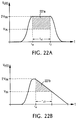
- One way to reset the saturable inductor to forward saturation is to simply turn on the unidirectional switch 130. Assume, for example, that the saturable inductor is in reverse saturation and that a new operating cycle is started. Closure of the switch 130 ( Figure 17) will result in application of Vin across the composite inductor; the saturable inductor 250 will become unsaturated as it begins to traverse a path like that of path 225 in Figure 18 and, as shown in Figure 21A, the application of Vin across the unsaturated inductor will result in a small positive flow of current Iin between times to and tf.
- the time period Ts2 in Figure 22B will be twice Ts1, since the volt-seconds associated with each of the areas 221a, 223b, and hence the two areas themselves, must be the same.
- the value of Ts will vary over an approximately 2 to 1 range as converter load is increased from no-load to Px.
- the delay time Treset will decline toward zero.
- Figure 23A and 23B Other ways to reset the saturable inductor, which will also reduce or eliminate the delay time of Figure 22, are illustrated in Figure 23A and 23B.
- the multi-mode switch of Figure 17 is modified by the addition of a diode 238.
- Use of this diode is generally beneficial as it will help control voltages and current flows when the unidirectional switch 130 is turned off. For example, if the switch 130 is turned off when a small positive current Iin is flowing, the diode 238 will provide a path for the flow of the current and clamp the voltage Vs at ground, thereby providing path for the flow of Iin toward the capacitor 42 and protecting the switch 130 from exposure to uncontrolled negative transient voltages.
- a resistor 237 and a diode 240 are connected from the converter output back to the saturable inductor 250 such that current, Ix, can flow from the output and through the inductor 250 in a direction which resets the inductor to forward saturation during the latter portion of the operating cycle when the voltage Vc is below Vout.
- FIG. 18 The operation of the multi-mode switch 200 of Figure 17 was explained with reference to the magnetization characteristic of Figure 18. This was done for purposes of illustration, but it is understood that the principle of operation of the switch is not dependent on a specific magnetization characteristic but rather on the impedance variation afforded by the reversion of the saturable inductor between its saturated and unsaturated states.
- saturable inductors having a variety of characteristics may be used.
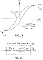
- Figure 24 shows a magnetization characteristic for a saturable inductor 350 which exhibits a saturated inductance, Lsat1, and a relatively smooth increase in inductance as current declines toward zero.
- the multi-mode switch 300 of Figure 25 consists of a unidirectional switch 130 in series with a saturable inductor 350 having a magnetization characteristic like that of Figure 24 for which, as indicated in Figure 25, the value of Lsat1 is approximately equal to a value Lr1, where Lr1 is significantly lower than the unsaturated inductance.
- the switch 300 may be applied in the same manner as the switch 200 of Figure 17.
- a benefit of the multi-mode switch topology 200 of Figure 17 is that the saturable inductor 250 provides reverse blocking with significantly less circuit loss than a series diode.
- a series Schottky blocking diode (used, as shown in Figure 5B, in conjunction with an N-channel MOSFET unidirectional switch 26) having a relatively low voltage drop of approximately 0.45 volt exhibits a loss of nearly 6 watts.
- the inductor loss is less than 1 Watt -- a reduction in overall loss of more than 5 Watts.
- Another benefit is that the performance of the ZCS switch controller can be relaxed. While the performance of the "ideal" converter of Figure 1 will depend upon the degree to which the timing of the turn-off of the switch coincides with the instant in time at which the current crosses zero, the accuracy of switch timing in converters which include series elements for blocking reverse current flow (such as prior art converters using switches of the kind shown in Figures 5B, 6B, or converters according to the present invention using switches of the kind shown in Figure 16 or 17) is much less important.
- the switch can be turned off at any time between the first zero crossing of current and the time at which the voltage Vc declines to a value Vin. If this timing condition is met, the diode 38 will block reverse current flow and the requirements for zero-current switching will be met.
- the unidirectional switch can be turned off at any time after the initial half-wave forward flow of current is complete but before the saturable inductor saturates.
- the simple dual-mode controller 112 illustrated in Figures 11A and 11B does not provide the bounded variation in lower frequency limit afforded by the use of a saturable inductor. Because the controller of Figure 11 incorporates a fixed delay time (e.g., delay time Td, Figure 12D), a converter using such a controller will exhibit a range of variation of operating frequency which is also dependent upon input voltage. As a result, the total range of variation will be approximately two times the anticipated variation in the value of Vin.
- a dual-mode controller can be arranged in a virtually infinite number of ways to provide for some desired behavior in converter minimum operating frequency.
- the dual-mode controller 112a of Figure 11C is arranged to emulate an ideal saturable inductor when used in a multi-mode switch of the kind shown in Figure 11A.
- each incoming trigger pulse 77 initiates a half-wave forward transfer phase via ZCS controller 12a.
- the integrator is enabled and begins to deliver an output, VS(t), proportional to the time integral of Vc(t).
- Vc(t) remains above Vin for a period of time sufficient for VS(t) to exceed some predetermined value, VS (equivalent to a volt-second rating), then the output of comparator 382 will go high, triggering monostable 76 and beginning a reverse energy transfer phase via ZCS controller 12b. If, however, the load is sufficiently high so that Vc(t) drops below Vin prior to VS(t) becoming greater than VS, then the output of comparator 70 will go low, the integrator 380 will be disabled and its output reset to zero, and the reverse energy transfer phase will not occur.
- Figure 26A shows a prior art ZCS boost converter 370
- Figure 26B shows waveforms for the voltage Vc(t) in the converter, when operated in the half-wave mode, as the load is reduced from the maximum allowable load value, Pmax, to lower values, P1>P2>P3, at a constant output voltage Vout>Vin.
- the operating frequency of the boost converter 370 will decline essentially linearly with load.
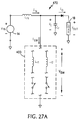
- FIG 27A shows a dual-mode ZCS boost converter 470 which corresponds to the topology of Figure 26A but which is modified to include a multi-mode switch 400.
- the switch can be of the kind shown in Figures 11, 14 or 16A-16D, incorporating a dual-mode switch controller (not shown, but of the kind previously described) for controlling the forward and reverse flow of switch current, Isw, or it can be a switch of the kind shown in Figures 17 and 25, using a saturable inductor.
- the converter 470 will operate in a half-wave mode: the switch 400 will be opened upon the first zero-crossing of current, Isw, following switch closure and only positive Isw will flow.
- the voltage Vc(t) will appear as shown in Figure 26B.
- a dual-mode ZCS boost converter will provide the same benefits previously described for the dual-mode ZCS buck configuration: by setting a lower bound on converter operating frequency it allows for a smaller, more efficient, converter; in configurations using a saturable inductor in the multi-mode switch, the full efficiency potential of half-wave ZCS conversion, at elevated loads, may be more closely achieved.
- the invention is also applicable to ZCS converters which operate directly from bipolar input sources.
- a converter of the kind described in our aforesaid EP-A-0692863, is shown in Figure 28.
- the voltage, Vin, delivered by the bipolar input source 214 may assume either positive or negative values.
- a bipolor switch 430 e.g., one which is capable of blocking a bipolar voltage, Vsw, when open, and capable of conducting a bipolar current, Isw, when closed
- Vsw bipolar voltage
- Isw bipolar current
- Figure 29 shows a dual-mode ZCS AC to DC boost converter 570 which corresponds to the topology of Figure 28 but which is modified to include a multi-mode switch 500. Since the multi-mode switch 500 must be a bipolar switch, multi-mode switches of the kind shown in Figures 11, 14 and 16A-16D may be used, but switches of the kind shown in Figures 17 and 25 may not.
- switches of the kind shown in Figures 11, 16A and 16C provide no apparent benefit over those in Figures 14, 16B and 16D, since the values of the two inductors 27a, 27b must be set to the same value (because the roles of the two switches 130a, 130b, will reverse with the polarity of the source in terms of whether they carry energy forward from the input source toward the load or in reverse back from the capacitor 442 to the input source).
- two bipolar multi-mode switches e.g., of the kind shown in Figure 16B
- inductors of different values may be paralleled and controlled in accordance with the polarity of the input source to.
- Bipolar multi-mode switches of the kind shown in Figures 30A and 30B incorporating unidirectional switches 130a, 130b and diodes 434a, 434b, 438a, 438b in combination with either a saturable inductor 450 alone, or a saturable inductor in series with a linear inductor 427, may also be used in bipolar ZCS dual-mode converters. While the saturable inductors cannot replace the series blocking diodes in a bipolar ZCS dual-mode converter, their volt-second rating can be used to provide the "timing" of the automatic initiation of the reverse energy transfer phase as load is reduced.
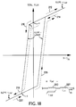
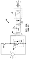
- Figure 31 shows an isolated half-wave ZCS forward converter 480 of the kind described in Vinciarelli, "Forward Converter Switching at Zero-Current," U. S. Patent No. 4,415,959, November, 1983 (incorporated by reference).
- the converter includes a circuit 490 for resetting the magnetic core of the transformer of the kind described in Vinciarelli, "Optimal Resetting of the Transformer's Core in Single Ended Forward Converters," U. S. Patent No. 4,441,146, April, 1984 (incorporated by reference).
- the characteristic time constant for the converter is set by the value of the transformer 464 leakage inductance, Ll, and the value of the capacitor 466, Cr.
- the main switch 460 is turned on and off at times when the forward current, Iin, is zero, and the reset switch 462 is controlled to be on when the main switch is off and to turn off prior to the main switch turning on.
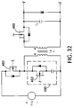
- a dual-mode version of the ZCS converter 492 of Figure 31A is shown in Figure 31B.
- the diode of Figure 31A has been replaced with a second switch 469.
- a dual-mode controller 112 e.g., of the kind shown in Figures 11A and 11B
- the reset switch 490 is controlled as in the prior art converter: it is turned on when the main switch is off and is turned off just prior to the main switch turning on.
- all of the switches 460, 469, 490 can be embodied as unidirectional switches, as is illustrated using MOSFETs in the partial schematic in Figure 32.
- a dual-mode ZCS power converter would typically include: (1) a switching element combined with circuit elements (e.g., inductors, capacitors), the circuit elements serving to both define the characteristic time constant(s) for the rise and fall of the currents and voltages in the converter during each converter operating cycle and arranged so that the switching element may be opened and closed at times of zero current, and (2) means for performing dual-mode control of the switching element. Dual-mode control provides for two distinct operating modes.
- circuit elements e.g., inductors, capacitors
- a switching element In a first operating mode a switching element is closed and opened once during each operating cycle, at consecutive times of zero current, to initiate a forward transfer of energy from the input source toward the load; in a second operating mode, a first closing and opening of a switching element, at consecutive times of zero current during a first phase of the operating cycle, associated with initiation of forward energy transfer from the input source toward the load, is followed a finite time later by a second phase during which a switching element is once again closed and opened at consecutive times of zero current, provided that operating conditions within the converter will allow for a reverse transfer of energy back to the input source.
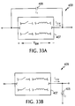
- the multi-mode switch may, as illustrated in Figures 33A and 33B, be generalized into a family of multi-mode resonant switches.
- the dual-mode resonant switch of Figure 33A is referred to as an M-Type dual-mode resonant switch 403 and the dual-mode resonant switch of Figure 33B is referred to as an L-Type dual-mode resonant switch 409.
- Both the M-Type and the L-Type dual-mode resonant switches include a multi-mode switch 407 and a capacitor 405.
- the multi-mode switch 407 can be any of the ones shown in Figures 11, 14 or 16A-16D, incorporating a dual-mode switch controller (not shown, but of the kind previously described) for controlling the forward and reverse flow of switch current, Isw, or it can be a switch of the kind shown in Figures 17, 25, 30A and 30B, using a saturable inductor.
- inductance included in series with the switching element within the multi-mode switch 407 provides for closing of the switching element at times of zero current and a limit on the rate-of-change of switch current thereafter; the combination of the inductance and the capacitance 405 causes a sinusoidal time variation in the switch current, thereby providing a zero-crossing of current, subsequent to turn-on, at which to turn the switching element off.
- the dual-mode switch controller provides for two distinct operating modes for the dual-mode resonant switches 403, 409.
- a switching element within the multi-mode switch 407 is closed and opened once during each operating cycle, at consecutive times of zero current, to initiate a flow of current, Isw, of a particular polarity; in a second operating mode, the first closing and opening of a switching element, at consecutive times of zero current during a first phase of the operating cycle associated with initiation of a flow of Isw at a particular polarity, is followed a finite time later by a second phase during which a switching element in the multi-mode switch 407 is closed and opened at consecutive times of zero current, provided that the second phase will allow for a flow of current Isw of an opposite polarity.
- any ZCS power conversion topology which can be operated in the full-wave operating mode can be adapted to dual-mode control.
Landscapes
- Engineering & Computer Science (AREA)
- Power Engineering (AREA)
- Dc-Dc Converters (AREA)
Applications Claiming Priority (2)
| Application Number | Priority Date | Filing Date | Title |
|---|---|---|---|
| US08/449,698 US5663635A (en) | 1995-05-24 | 1995-05-24 | Reverse energy transfer in zero-current switching power conversion |
| US449698 | 1995-05-24 |
Publications (3)
| Publication Number | Publication Date |
|---|---|
| EP0744817A2 true EP0744817A2 (fr) | 1996-11-27 |
| EP0744817A3 EP0744817A3 (fr) | 1997-10-01 |
| EP0744817B1 EP0744817B1 (fr) | 2001-10-24 |
Family
ID=23785140
Family Applications (1)
| Application Number | Title | Priority Date | Filing Date |
|---|---|---|---|
| EP96303034A Expired - Lifetime EP0744817B1 (fr) | 1995-05-24 | 1996-04-30 | Transfert inverse d'énergie dans un convertisseur de puissance à commutation par courant nul |
Country Status (4)
| Country | Link |
|---|---|
| US (2) | US5663635A (fr) |
| EP (1) | EP0744817B1 (fr) |
| JP (1) | JP2868148B2 (fr) |
| DE (1) | DE69616149T2 (fr) |
Cited By (2)
| Publication number | Priority date | Publication date | Assignee | Title |
|---|---|---|---|---|
| EP0825699A3 (fr) * | 1996-08-01 | 1999-04-14 | Benchmarq Microelectronics, Inc. | Régulateur à découpage avec réglage de phase pour un sectionneur de puissance |
| EP3541650B1 (fr) * | 2016-11-21 | 2020-12-23 | Rutronik Elektronische Bauelemente GmbH | Système de stockage d'énergie hybride |
Families Citing this family (52)
| Publication number | Priority date | Publication date | Assignee | Title |
|---|---|---|---|---|
| US5929692A (en) * | 1997-07-11 | 1999-07-27 | Computer Products Inc. | Ripple cancellation circuit with fast load response for switch mode voltage regulators with synchronous rectification |
| JP3657445B2 (ja) * | 1998-01-28 | 2005-06-08 | セイコーインスツル株式会社 | 電子機器 |
| US5932995A (en) * | 1998-03-03 | 1999-08-03 | Magnetek, Inc. | Dual buck converter with coupled inductors |
| US6184666B1 (en) * | 1998-03-09 | 2001-02-06 | 3Dlabs Inc. Ltd. | Buck converter with parallel switches |
| US5923143A (en) * | 1998-03-20 | 1999-07-13 | York International Corporation | Solid state motor starter with energy recovery |
| EP1061628B1 (fr) * | 1999-06-16 | 2004-12-08 | STMicroelectronics S.r.l. | Circuit d'interconnexion d'un autoradio et d'un accumulateur d'automobile |
| US6377477B1 (en) | 1999-07-16 | 2002-04-23 | University Of Hong Kong | Self-driven synchronous rectifier by retention of gate charge |
| US6144565A (en) * | 1999-07-20 | 2000-11-07 | Semtech Corporation | Variation on a single-ended primary inductor converter |
| US6252383B1 (en) * | 2000-07-11 | 2001-06-26 | Technical Witts, Inc. | Buck and boost power converters with non-pulsating input and output terminal currents |
| US6472852B1 (en) | 2000-11-02 | 2002-10-29 | Semtech Corporation | Resonant buck-type voltage converter using swinging inductance |
| US7049786B1 (en) * | 2002-11-25 | 2006-05-23 | The Texas A&M University System | Unipolar drive topology for permanent magnet brushless DC motors and switched reluctance motors |
| US6989997B2 (en) * | 2003-06-25 | 2006-01-24 | Virginia Tech Intellectual Properties, Inc. | Quasi-resonant DC-DC converters with reduced body diode loss |
| US7262521B2 (en) * | 2003-12-31 | 2007-08-28 | Pratt & Whitney Canada Corp. | Variable AC voltage regulation control method and apparatus |
| US7133299B2 (en) * | 2004-01-09 | 2006-11-07 | Pi International Ltd. | Zero voltage switching power conversion circuit |
| DE102004061341A1 (de) * | 2004-12-20 | 2006-07-06 | Puls Gmbh | Stromversorgung |
| JP4877459B2 (ja) * | 2005-06-01 | 2012-02-15 | ミツミ電機株式会社 | 電流共振型マルチフェーズdc/dcコンバータおよびその制御方法 |
| JP2007006669A (ja) * | 2005-06-27 | 2007-01-11 | Mitsumi Electric Co Ltd | 電流共振型マルチフェーズdc/dcコンバータおよびその制御方法 |
| JP2007020305A (ja) * | 2005-07-07 | 2007-01-25 | Toshiba Corp | パルス電源装置 |
| JP2007028830A (ja) * | 2005-07-19 | 2007-02-01 | Mitsumi Electric Co Ltd | スイッチング電源およびその制御方法 |
| JP2007028829A (ja) * | 2005-07-19 | 2007-02-01 | Mitsumi Electric Co Ltd | 電流共振型dc/dcコンバータおよびその共振電流制御方法 |
| JP4636249B2 (ja) * | 2005-07-19 | 2011-02-23 | ミツミ電機株式会社 | 電流共振型dc/dcコンバータおよびそのゼロ電流スイッチング実現方法 |
| JP4711060B2 (ja) * | 2005-09-07 | 2011-06-29 | ミツミ電機株式会社 | 電流共振型dc/dcコンバータ、それに使用される電流検出回路、および電流検出方法 |
| KR100984827B1 (ko) * | 2008-09-30 | 2010-10-04 | 전남대학교산학협력단 | 최소 리액터를 이용한 다중레벨 dc/dc컨버터 |
| JP5227157B2 (ja) * | 2008-12-22 | 2013-07-03 | トヨタ自動車株式会社 | 共振型dc−dcコンバータ |
| US8669744B1 (en) * | 2011-02-15 | 2014-03-11 | Vlt, Inc. | Adaptive control of switching losses in power converters |
| US8773085B2 (en) | 2011-03-22 | 2014-07-08 | Ledillion Technologies Inc. | Apparatus and method for efficient DC-to-DC conversion through wide voltage swings |
| TW201406038A (zh) * | 2012-07-24 | 2014-02-01 | Hon Hai Prec Ind Co Ltd | 整流電路 |
| CN102830740B (zh) * | 2012-08-23 | 2014-04-30 | 矽力杰半导体技术(杭州)有限公司 | 一种高效率的偏置电压产生电路 |
| US20140119058A1 (en) * | 2012-10-30 | 2014-05-01 | Chicony Power Technology Co., Ltd. | Power voltage conversion system for controller integrated circuit |
| EP2994987A4 (fr) * | 2013-05-10 | 2017-04-19 | Rompower Energy Systems, Inc. | Transfert indirect à commande de transition résonante |
| US9407154B2 (en) * | 2013-06-14 | 2016-08-02 | Advanced Charging Technologies, LLC | Electrical circuit for delivering power to consumer electronic devices |
| JP6037971B2 (ja) * | 2013-08-09 | 2016-12-07 | 三菱電機株式会社 | 降圧チョッパ回路 |
| CN104578768B (zh) * | 2013-10-22 | 2018-10-02 | 南京中兴新软件有限责任公司 | 一种直流电源及其工作方法 |
| KR102120955B1 (ko) * | 2013-11-22 | 2020-06-10 | 삼성전자주식회사 | 시간 지연 기법을 이용하여 역전류 누설을 제거하는 역전류 보상 회로 및 능동형 정류기 |
| US10298071B2 (en) * | 2014-03-05 | 2019-05-21 | Ricoh Co., Ltd | DC-DC boost converter |
| US9793807B2 (en) * | 2015-03-22 | 2017-10-17 | Boris Ablov | Lossless power conversion to DC method and device |
| US9712055B1 (en) * | 2015-10-21 | 2017-07-18 | Picor Corporation | Zero voltage switching energy recovery control of discontinuous PWM switching power converters |
| US10193442B2 (en) | 2016-02-09 | 2019-01-29 | Faraday Semi, LLC | Chip embedded power converters |
| US10340803B2 (en) * | 2016-04-22 | 2019-07-02 | Texas Instruments Incorporated | DC-DC converter having predicted zero inductor current |
| KR101923690B1 (ko) * | 2016-11-11 | 2018-11-29 | 엘에스산전 주식회사 | 전력보상장치의 서브모듈성능시험을 위한 합성시험회로 및 그 시험방법 |
| FR3060904B1 (fr) * | 2016-12-15 | 2023-10-27 | 3D Plus | Convertisseur de tension haute frequence continue de type buck quasi-resonant |
| US10763668B2 (en) * | 2017-11-01 | 2020-09-01 | Mediatek Inc. | Converter with inductors coupled in series |
| US10250143B1 (en) * | 2018-08-07 | 2019-04-02 | Monolithic Power Systems, Inc. | AC-DC converting apparatus and method thereof |
| US10504848B1 (en) | 2019-02-19 | 2019-12-10 | Faraday Semi, Inc. | Chip embedded integrated voltage regulator |
| US11069624B2 (en) | 2019-04-17 | 2021-07-20 | Faraday Semi, Inc. | Electrical devices and methods of manufacture |
| DE102019214674A1 (de) * | 2019-09-25 | 2020-12-17 | Siemens Healthcare Gmbh | Stromrichterschaltung und Verfahren zur Umwandlung elektrischer Signale |
| US11101640B1 (en) * | 2020-07-29 | 2021-08-24 | Abb Schweiz | Solid-state protection for direct current networks |
| US11063516B1 (en) | 2020-07-29 | 2021-07-13 | Faraday Semi, Inc. | Power converters with bootstrap |
| CN114158221B (zh) | 2021-11-30 | 2024-06-28 | 杭州云电科技能源有限公司 | 同步整流模块 |
| CN114094369B (zh) | 2021-11-30 | 2024-09-10 | 杭州云电科技能源有限公司 | 同步整流组件、其制作方法及电源 |
| US11990839B2 (en) | 2022-06-21 | 2024-05-21 | Faraday Semi, Inc. | Power converters with large duty cycles |
| CN115313332B (zh) * | 2022-08-12 | 2025-04-11 | 杭州云电科技能源有限公司 | 有源限流电路、电源装置、供电系统以及控制方法 |
Family Cites Families (9)
| Publication number | Priority date | Publication date | Assignee | Title |
|---|---|---|---|---|
| US4415959A (en) * | 1981-03-20 | 1983-11-15 | Vicor Corporation | Forward converter switching at zero current |
| US4441146A (en) * | 1982-02-04 | 1984-04-03 | Vicor Corporation | Optimal resetting of the transformer's core in single ended forward converters |
| US4720667A (en) * | 1986-06-20 | 1988-01-19 | Lee Fred C | Zero-current switching quasi-resonant converters operating in a full-wave mode |
| JP2773195B2 (ja) * | 1988-04-05 | 1998-07-09 | 松下電器産業株式会社 | スイッチング電源装置 |
| US4829232A (en) * | 1988-09-02 | 1989-05-09 | General Motors Corporation | Nonlinear resonant switch and converter |
| US5235502A (en) * | 1989-11-22 | 1993-08-10 | Vlt Corporation | Zero current switching forward power conversion apparatus and method with controllable energy transfer |
| US5321348A (en) * | 1991-03-08 | 1994-06-14 | Vlt Corporation | Boost switching power conversion |
| US5432431A (en) * | 1992-05-21 | 1995-07-11 | Vlt Corporation | Boost switching power conversion using saturable inductors |
| US5486752A (en) * | 1994-06-17 | 1996-01-23 | Center For Innovative Technology** | Zero-current transition PWM converters |
-
1995
- 1995-05-24 US US08/449,698 patent/US5663635A/en not_active Expired - Lifetime
- 1995-06-02 US US08/459,126 patent/US5668466A/en not_active Expired - Lifetime
-
1996
- 1996-04-30 EP EP96303034A patent/EP0744817B1/fr not_active Expired - Lifetime
- 1996-04-30 DE DE69616149T patent/DE69616149T2/de not_active Expired - Fee Related
- 1996-05-24 JP JP8129423A patent/JP2868148B2/ja not_active Expired - Fee Related
Cited By (4)
| Publication number | Priority date | Publication date | Assignee | Title |
|---|---|---|---|---|
| EP0825699A3 (fr) * | 1996-08-01 | 1999-04-14 | Benchmarq Microelectronics, Inc. | Régulateur à découpage avec réglage de phase pour un sectionneur de puissance |
| US6072708A (en) * | 1996-08-01 | 2000-06-06 | Benchmarq Microelectronics, Inc. | Phase controlled switching regulator power supply |
| EP3541650B1 (fr) * | 2016-11-21 | 2020-12-23 | Rutronik Elektronische Bauelemente GmbH | Système de stockage d'énergie hybride |
| US10951025B2 (en) | 2016-11-21 | 2021-03-16 | Rutronik Elektronische Bauelemente Gmbh | Hybrid energy storage system |
Also Published As
| Publication number | Publication date |
|---|---|
| DE69616149D1 (de) | 2001-11-29 |
| JP2868148B2 (ja) | 1999-03-10 |
| EP0744817A3 (fr) | 1997-10-01 |
| US5668466A (en) | 1997-09-16 |
| US5663635A (en) | 1997-09-02 |
| JPH09103070A (ja) | 1997-04-15 |
| DE69616149T2 (de) | 2002-03-07 |
| EP0744817B1 (fr) | 2001-10-24 |
Similar Documents
| Publication | Publication Date | Title |
|---|---|---|
| EP0744817B1 (fr) | Transfert inverse d'énergie dans un convertisseur de puissance à commutation par courant nul | |
| US5959438A (en) | Soft-switched boost converter with isolated active snubber | |
| US5438498A (en) | Series resonant converter having a resonant snubber | |
| US5434767A (en) | Power converter possessing zero-voltage switching and output isolation | |
| EP0123147B1 (fr) | Convertisseur de courant continu stabilisé | |
| US5132889A (en) | Resonant-transition DC-to-DC converter | |
| US5430633A (en) | Multi-resonant clamped flyback converter | |
| US4713742A (en) | Dual-inductor buck switching converter | |
| US5894412A (en) | System with open-loop DC-DC converter stage | |
| US5539630A (en) | Soft-switching converter DC-to-DC isolated with voltage bidirectional switches on the secondary side of an isolation transformer | |
| US6147886A (en) | Dual opposed interleaved coupled inductor soft switching converters | |
| US7518895B2 (en) | High-efficiency power converter system | |
| US5781419A (en) | Soft switching DC-to-DC converter with coupled inductors | |
| KR100186776B1 (ko) | 직류/직류 스위칭 변환기 회로 | |
| US6208529B1 (en) | Zero voltage switching buck derived converter | |
| US6987675B2 (en) | Soft-switched power converters | |
| US9407156B2 (en) | Managing leakage inductance in a power supply | |
| US5268830A (en) | Drive circuit for power switches of a zero-voltage switching power converter | |
| US4845605A (en) | High-frequency DC-DC power converter with zero-voltage switching of single primary-side power device | |
| EP0610158A1 (fr) | Convertisseur à découpage à tension nulle et à fréquence fixe | |
| US20010036088A1 (en) | Efficient power conversion circuit having zero voltage switching | |
| US20040145273A1 (en) | Electronic driver circuit for high-speed actuation of high-capacitance actuators | |
| US7272020B2 (en) | Isolated, current-fed, pulse width modulation, DC-DC converter | |
| KR930000966B1 (ko) | 비선형 공진스위치 및 콘버터 | |
| US5870291A (en) | Asymmetrical half-bridge converter having adjustable parasitic resistances to offset output voltage DC bias |
Legal Events
| Date | Code | Title | Description |
|---|---|---|---|
| PUAI | Public reference made under article 153(3) epc to a published international application that has entered the european phase |
Free format text: ORIGINAL CODE: 0009012 |
|
| AK | Designated contracting states |
Kind code of ref document: A2 Designated state(s): DE FR GB |
|
| PUAL | Search report despatched |
Free format text: ORIGINAL CODE: 0009013 |
|
| AK | Designated contracting states |
Kind code of ref document: A3 Designated state(s): DE FR GB |
|
| 17P | Request for examination filed |
Effective date: 19980115 |
|
| GRAG | Despatch of communication of intention to grant |
Free format text: ORIGINAL CODE: EPIDOS AGRA |
|
| 17Q | First examination report despatched |
Effective date: 20000920 |
|
| GRAG | Despatch of communication of intention to grant |
Free format text: ORIGINAL CODE: EPIDOS AGRA |
|
| GRAG | Despatch of communication of intention to grant |
Free format text: ORIGINAL CODE: EPIDOS AGRA |
|
| GRAH | Despatch of communication of intention to grant a patent |
Free format text: ORIGINAL CODE: EPIDOS IGRA |
|
| GRAH | Despatch of communication of intention to grant a patent |
Free format text: ORIGINAL CODE: EPIDOS IGRA |
|
| GRAA | (expected) grant |
Free format text: ORIGINAL CODE: 0009210 |
|
| AK | Designated contracting states |
Kind code of ref document: B1 Designated state(s): DE FR GB |
|
| REF | Corresponds to: |
Ref document number: 69616149 Country of ref document: DE Date of ref document: 20011129 |
|
| REG | Reference to a national code |
Ref country code: GB Ref legal event code: IF02 |
|
| ET | Fr: translation filed | ||
| PLBE | No opposition filed within time limit |
Free format text: ORIGINAL CODE: 0009261 |
|
| STAA | Information on the status of an ep patent application or granted ep patent |
Free format text: STATUS: NO OPPOSITION FILED WITHIN TIME LIMIT |
|
| 26N | No opposition filed | ||
| PGFP | Annual fee paid to national office [announced via postgrant information from national office to epo] |
Ref country code: FR Payment date: 20050418 Year of fee payment: 10 |
|
| PGFP | Annual fee paid to national office [announced via postgrant information from national office to epo] |
Ref country code: GB Payment date: 20050427 Year of fee payment: 10 |
|
| PGFP | Annual fee paid to national office [announced via postgrant information from national office to epo] |
Ref country code: DE Payment date: 20050531 Year of fee payment: 10 |
|
| PG25 | Lapsed in a contracting state [announced via postgrant information from national office to epo] |
Ref country code: GB Free format text: LAPSE BECAUSE OF NON-PAYMENT OF DUE FEES Effective date: 20060430 |
|
| PG25 | Lapsed in a contracting state [announced via postgrant information from national office to epo] |
Ref country code: DE Free format text: LAPSE BECAUSE OF NON-PAYMENT OF DUE FEES Effective date: 20061101 |
|
| GBPC | Gb: european patent ceased through non-payment of renewal fee |
Effective date: 20060430 |
|
| REG | Reference to a national code |
Ref country code: FR Ref legal event code: ST Effective date: 20061230 |
|
| PG25 | Lapsed in a contracting state [announced via postgrant information from national office to epo] |
Ref country code: FR Free format text: LAPSE BECAUSE OF NON-PAYMENT OF DUE FEES Effective date: 20060502 |