EP0745873A2 - Optischer Wellenleitermodule und Verfahren zu seiner Herstellung - Google Patents
Optischer Wellenleitermodule und Verfahren zu seiner Herstellung Download PDFInfo
- Publication number
- EP0745873A2 EP0745873A2 EP96108454A EP96108454A EP0745873A2 EP 0745873 A2 EP0745873 A2 EP 0745873A2 EP 96108454 A EP96108454 A EP 96108454A EP 96108454 A EP96108454 A EP 96108454A EP 0745873 A2 EP0745873 A2 EP 0745873A2
- Authority
- EP
- European Patent Office
- Prior art keywords
- waveguide
- cladding region
- region
- flexible substrate
- optical waveguide
- Prior art date
- Legal status (The legal status is an assumption and is not a legal conclusion. Google has not performed a legal analysis and makes no representation as to the accuracy of the status listed.)
- Granted
Links
Images

Classifications
-
- G—PHYSICS
- G02—OPTICS
- G02B—OPTICAL ELEMENTS, SYSTEMS OR APPARATUS
- G02B6/00—Light guides; Structural details of arrangements comprising light guides and other optical elements, e.g. couplings
- G02B6/24—Coupling light guides
- G02B6/42—Coupling light guides with opto-electronic elements
- G02B6/4201—Packages, e.g. shape, construction, internal or external details
- G02B6/4246—Bidirectionally operating package structures
-
- G—PHYSICS
- G02—OPTICS
- G02B—OPTICAL ELEMENTS, SYSTEMS OR APPARATUS
- G02B6/00—Light guides; Structural details of arrangements comprising light guides and other optical elements, e.g. couplings
- G02B6/10—Light guides; Structural details of arrangements comprising light guides and other optical elements, e.g. couplings of the optical waveguide type
- G02B6/12—Light guides; Structural details of arrangements comprising light guides and other optical elements, e.g. couplings of the optical waveguide type of the integrated circuit kind
- G02B6/122—Basic optical elements, e.g. light-guiding paths
- G02B6/1221—Basic optical elements, e.g. light-guiding paths made from organic materials
-
- G—PHYSICS
- G02—OPTICS
- G02B—OPTICAL ELEMENTS, SYSTEMS OR APPARATUS
- G02B6/00—Light guides; Structural details of arrangements comprising light guides and other optical elements, e.g. couplings
- G02B6/24—Coupling light guides
- G02B6/26—Optical coupling means
- G02B6/30—Optical coupling means for use between fibre and thin-film device
-
- G—PHYSICS
- G02—OPTICS
- G02B—OPTICAL ELEMENTS, SYSTEMS OR APPARATUS
- G02B6/00—Light guides; Structural details of arrangements comprising light guides and other optical elements, e.g. couplings
- G02B6/24—Coupling light guides
- G02B6/42—Coupling light guides with opto-electronic elements
-
- G—PHYSICS
- G02—OPTICS
- G02B—OPTICAL ELEMENTS, SYSTEMS OR APPARATUS
- G02B6/00—Light guides; Structural details of arrangements comprising light guides and other optical elements, e.g. couplings
- G02B6/24—Coupling light guides
- G02B6/42—Coupling light guides with opto-electronic elements
- G02B6/4201—Packages, e.g. shape, construction, internal or external details
- G02B6/4219—Mechanical fixtures for holding or positioning the elements relative to each other in the couplings; Alignment methods for the elements, e.g. measuring or observing methods especially used therefor
- G02B6/4236—Fixing or mounting methods of the aligned elements
-
- G—PHYSICS
- G02—OPTICS
- G02B—OPTICAL ELEMENTS, SYSTEMS OR APPARATUS
- G02B6/00—Light guides; Structural details of arrangements comprising light guides and other optical elements, e.g. couplings
- G02B6/24—Coupling light guides
- G02B6/42—Coupling light guides with opto-electronic elements
- G02B6/4201—Packages, e.g. shape, construction, internal or external details
- G02B6/4249—Packages, e.g. shape, construction, internal or external details comprising arrays of active devices and fibres
-
- G—PHYSICS
- G02—OPTICS
- G02B—OPTICAL ELEMENTS, SYSTEMS OR APPARATUS
- G02B6/00—Light guides; Structural details of arrangements comprising light guides and other optical elements, e.g. couplings
- G02B6/24—Coupling light guides
- G02B6/42—Coupling light guides with opto-electronic elements
- G02B6/4201—Packages, e.g. shape, construction, internal or external details
- G02B6/4266—Thermal aspects, temperature control or temperature monitoring
- G02B6/4268—Cooling
- G02B6/4272—Cooling with mounting substrates of high thermal conductivity
-
- G—PHYSICS
- G02—OPTICS
- G02B—OPTICAL ELEMENTS, SYSTEMS OR APPARATUS
- G02B6/00—Light guides; Structural details of arrangements comprising light guides and other optical elements, e.g. couplings
- G02B6/24—Coupling light guides
- G02B6/42—Coupling light guides with opto-electronic elements
- G02B6/4201—Packages, e.g. shape, construction, internal or external details
- G02B6/4274—Electrical aspects
- G02B6/428—Electrical aspects containing printed circuit boards [PCB]
- G02B6/4281—Electrical aspects containing printed circuit boards [PCB] the printed circuit boards being flexible
-
- G—PHYSICS
- G02—OPTICS
- G02B—OPTICAL ELEMENTS, SYSTEMS OR APPARATUS
- G02B6/00—Light guides; Structural details of arrangements comprising light guides and other optical elements, e.g. couplings
- G02B6/24—Coupling light guides
- G02B6/42—Coupling light guides with opto-electronic elements
- G02B6/4201—Packages, e.g. shape, construction, internal or external details
- G02B6/4274—Electrical aspects
- G02B6/4283—Electrical aspects with electrical insulation means
-
- H—ELECTRICITY
- H01—ELECTRIC ELEMENTS
- H01S—DEVICES USING THE PROCESS OF LIGHT AMPLIFICATION BY STIMULATED EMISSION OF RADIATION [LASER] TO AMPLIFY OR GENERATE LIGHT; DEVICES USING STIMULATED EMISSION OF ELECTROMAGNETIC RADIATION IN WAVE RANGES OTHER THAN OPTICAL
- H01S5/00—Semiconductor lasers
- H01S5/10—Construction or shape of the optical resonator, e.g. extended or external cavity, coupled cavities, bent-guide, varying width, thickness or composition of the active region
- H01S5/18—Surface-emitting [SE] lasers, e.g. having both horizontal and vertical cavities
- H01S5/183—Surface-emitting [SE] lasers, e.g. having both horizontal and vertical cavities having only vertical cavities, e.g. vertical cavity surface-emitting lasers [VCSEL]
-
- G—PHYSICS
- G02—OPTICS
- G02B—OPTICAL ELEMENTS, SYSTEMS OR APPARATUS
- G02B6/00—Light guides; Structural details of arrangements comprising light guides and other optical elements, e.g. couplings
- G02B6/24—Coupling light guides
- G02B6/42—Coupling light guides with opto-electronic elements
- G02B6/4201—Packages, e.g. shape, construction, internal or external details
- G02B6/4219—Mechanical fixtures for holding or positioning the elements relative to each other in the couplings; Alignment methods for the elements, e.g. measuring or observing methods especially used therefor
- G02B6/422—Active alignment, i.e. moving the elements in response to the detected degree of coupling or position of the elements
- G02B6/4221—Active alignment, i.e. moving the elements in response to the detected degree of coupling or position of the elements involving a visual detection of the position of the elements, e.g. by using a microscope or a camera
- G02B6/4224—Active alignment, i.e. moving the elements in response to the detected degree of coupling or position of the elements involving a visual detection of the position of the elements, e.g. by using a microscope or a camera using visual alignment markings, e.g. index methods
-
- G—PHYSICS
- G02—OPTICS
- G02B—OPTICAL ELEMENTS, SYSTEMS OR APPARATUS
- G02B6/00—Light guides; Structural details of arrangements comprising light guides and other optical elements, e.g. couplings
- G02B6/24—Coupling light guides
- G02B6/42—Coupling light guides with opto-electronic elements
- G02B6/4201—Packages, e.g. shape, construction, internal or external details
- G02B6/4219—Mechanical fixtures for holding or positioning the elements relative to each other in the couplings; Alignment methods for the elements, e.g. measuring or observing methods especially used therefor
- G02B6/422—Active alignment, i.e. moving the elements in response to the detected degree of coupling or position of the elements
- G02B6/4227—Active alignment methods, e.g. procedures and algorithms
-
- G—PHYSICS
- G02—OPTICS
- G02B—OPTICAL ELEMENTS, SYSTEMS OR APPARATUS
- G02B6/00—Light guides; Structural details of arrangements comprising light guides and other optical elements, e.g. couplings
- G02B6/24—Coupling light guides
- G02B6/42—Coupling light guides with opto-electronic elements
- G02B6/4201—Packages, e.g. shape, construction, internal or external details
- G02B6/4266—Thermal aspects, temperature control or temperature monitoring
- G02B6/4268—Cooling
- G02B6/4269—Cooling with heat sinks or radiation fins
-
- H—ELECTRICITY
- H01—ELECTRIC ELEMENTS
- H01S—DEVICES USING THE PROCESS OF LIGHT AMPLIFICATION BY STIMULATED EMISSION OF RADIATION [LASER] TO AMPLIFY OR GENERATE LIGHT; DEVICES USING STIMULATED EMISSION OF ELECTROMAGNETIC RADIATION IN WAVE RANGES OTHER THAN OPTICAL
- H01S5/00—Semiconductor lasers
- H01S5/02—Structural details or components not essential to laser action
- H01S5/022—Mountings; Housings
- H01S5/023—Mount members, e.g. sub-mount members
- H01S5/02325—Mechanically integrated components on mount members or optical micro-benches
-
- H—ELECTRICITY
- H10—SEMICONDUCTOR DEVICES; ELECTRIC SOLID-STATE DEVICES NOT OTHERWISE PROVIDED FOR
- H10W—GENERIC PACKAGES, INTERCONNECTIONS, CONNECTORS OR OTHER CONSTRUCTIONAL DETAILS OF DEVICES COVERED BY CLASS H10
- H10W90/00—Package configurations
- H10W90/701—Package configurations characterised by the relative positions of pads or connectors relative to package parts
- H10W90/721—Package configurations characterised by the relative positions of pads or connectors relative to package parts of bump connectors
- H10W90/724—Package configurations characterised by the relative positions of pads or connectors relative to package parts of bump connectors between a chip and a stacked insulating package substrate, interposer or RDL
Definitions
- This invention relates, in general, to fabrication of optical devices and, more particularly, to interconnecting optical devices and waveguides together.
- conventional interconnection of an optical device and a waveguide typically is achieved by carefully aligning the optical device to the waveguide manually, commonly referred to as active alignment. Once the optical device is aligned to the waveguide, the optical device is affixed to the waveguide.
- active alignment Once the optical device is aligned to the waveguide, the optical device is affixed to the waveguide.
- problems arise by aligning the optical device and the waveguide manually, such as being extremely labor intensive, being costly, and being inaccurate.
- curing of an adhesive that affixes or binds the optical device to the waveguide often shift the alignment of the optical device to the waveguide, thereby causing inefficient transfer of light from the optical device.
- the misalignment is severe enough, unusable product is manufactured, thus increasing cost and reducing manufacturing capability.
- the optical device and the waveguide are then mounted onto an interconnect substrate.
- mounting of the optical device and the waveguide to the interconnect substrate also has several problems, such as fragility of the fixed optical device and waveguide, alignment capability of the optical device and waveguide to the interconnect substrate, electrical coupling of the optical device, and the like, thus making the interconnection of the optical device, the waveguide, and the interconnect substrate unsuitable for high volume manufacturing.
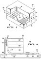
- FIG. 1 illustrates an enlarged simplified isometric view of a waveguide 10, with a portion 14 thereof removed.
- FIG. 1 illustrates an enlarged simplified isometric view of a waveguide 10, with a portion 14 thereof removed.
- dimensional control and relative sizing of waveguide 10 have been relaxed.
- Waveguide 10 is made of several elements or features, including cladding regions 11, 12, and 13, ends 23 and 24, a plurality of core regions 31 and 32, and an alignment guide 26.
- Cladding regions 11, 12, and 13 further include surfaces 21 and 22, 18 and 19, and 16 and 17, respectively.
- the plurality of core regions 31 and 32 is viewed with greater clarity. Additionally, it should be pointed out that the plurality of core regions 31 and 32 are surrounded by cladding regions 11 and 12 and 13 and 12, respectively.
- cladding regions 11, 12, and 13 and the plurality of core regions 31 and 32 are made by any suitable method or technique, such as milling, molding, laser ablating, filling, or the like.
- cladding regions 11, 12, and 13 are made by any suitable molding method or technique, such as injection molding, transfer molding, or the like.
- the plurality of core regions 31 and 32 is made by any suitable filling technique or method, such as press filling, capillary filling, hydraulic injection, or the like.
- cladding regions 11, 12, and 13 and the plurality of core regions 31 and 32 are made of any suitable polymer material or combination of materials, such as plastics, epoxies, polyimides, polyvinyl, or the like.
- cladding regions 11, 12, and 13 and the plurality of core regions 31 and 32 are made of an epoxy material.
- processing conditions for these materials range from 22-400 degrees Celsius for molding temperatures and 200-2,000 pounds per square inch for molding pressures.
- Refractive indexes for these materials range from 1.3 to 1.8, with a preferred range from 1.4 to 1.7; however, the plurality of core region have a higher refractive index than cladding regions 11, 12, and 13.
- Cladding regions 11, 12, and 13 are form so that cladding regions 11, 12, and 13 are stackable, thereby forming the plurality of core regions 31 and 32 surrounded by cladding regions 11, 12, and 13.
- alignment guide 26 is made by any suitable method, such as molding, milling, laser ablating, or the like. As shown in FIG. 1, alignment guide is illustrate as a ferule; however, it should be understood that alignment guide 26 can be any suitable shape, such as pins, keys or ways, or the like.
- cladding regions 11 and 13 are affixed to cladding region 12 by an optical adhesive.
- the optical adhesive is applied to either surface 18 or surface 17.
- Cladding regions 12 and 13 are pressed so that surface 17 and 18 are mated, thereby squeezing the optical adhesive throughout grooves 32 and adhering cladding regions 12 and 13.
- a similar procedure is followed for adhering cladding region 11 to cladding region 12.
- grooves 32 and 33 become the plurality of core regions 31 and 32 with cladding regions 11, 12, and 13 surrounding the plurality of core regions 31 and 32.
- grooves 33 and 34 can be formed on cladding regions 11 and 13 and subsequently adhered to cladding region 12.
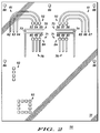
- Flexible substrate 51 is made of several elements or features, such as a plurality of bonding pads 52 including bonding pads 53-58, a plurality of electrical traces 61 including electrical traces 62-67, optically clear regions 70 and 71, electrical traces 73 and 74, a plurality of electrical traces 76 including electrical traces 77-82, a plurality of bonding pads 84, and alignment guides 86.
- the plurality of electrical traces 61 and 76, the plurality of bonding pads 52 and 84, and electrical traces 73 and 74 illustrate paths for electrical signals to travel throughout flexible substrate 51. It should be further understood that these electrical paths can be patterned in any suitable configuration on or in flexible substrate 51, thereby enabling electrical signals to be passed throughout flexible substrate 51.
- electrical control signals are carried by the plurality of electrical traces 61 and 76 to the plurality of bonding pads 52 and 84, while electrical traces 73 and 74 provide a ground.
- Flexible substrate 51 is made by any suitable method or technique.
- flexible substrate 51 is made from any thin insulative material, such as those suitable for tape automated bonding (TAB) backing layer or substrate.
- TAB tape automated bonding
- Polyimide is a representative material, but is certainly not the only one; polyimide may be found under tradenames such as "UPLEX” or "KAPTON", among others.
- suitable materials include, but are not necessarily limited to, polyester materials (lower in cost and performance that polyimide), mylar materials, and composite materials, e.g., a resin filled epoxy, a fiber reinforced material, and the like.
- the plurality of electrical traces 61 and 76, the plurality of bonding pads 52 and 84, and electrical traces 73 and 74 are formed by any suitable method, such as but not limited to plating, etching, photolithography, printing, etc.
- the plurality of electrical traces 61 and 76, the plurality of bonding pads 52 and 84, and electrical traces 73 and 74 are made of suitable electrically conductive material, such as a metal, e.g., aluminum (Al), titanium (Ti), copper (Cu), tungsten (W), silver (Ag), a metal alloy, e.g., titanium/tungsten (TiW), aluminum/copper (Al/Cu), an electrically conductive adhesive, e.g., silver filled epoxy, gold filled epoxy, copper filled epoxy, or the like.
- Adhesion of the plurality of electrical traces 61 and 76, the plurality of bonding pads 52 and 84, and electrical traces 73 and 74 to flexible substrate 51 is such that they will not delaminate or separate from flexible substrate 51 when flexible substrate 51 is bent or positioned in subsequent processing.
- materials selected for fabrication of insulative flexible substrate 51 generally are temperature resistant.
- flexible substrate 51 will undergo an overmolding process. Temperatures and times of duration of the overmolding process typically range from 200-300 degrees Celsius with time ranges from 10-15 minutes.
- material selected for fabrication of flexible substrate 51 needs to be able to tolerate these temperatures and times.
- materials that exceed these requirements or performance levels are also usable. While several manufacturers are capable of supplying flexible substrate 51, purchase of flexible substrate 51 is available from Rogers Corporation located in Arizona.
- Windows 70 and 71 are formed by any suitable method, such as removing a portion, corresponding to windows 70 and 71, from flexible substrate 51, making a portion, corresponding to windows 70 and 71, transparent, thereby providing an optically clear area in flexible substrate 51.
- the plurality of bonding pads 92 and 93 illustrate an ability for electrical coupling, i.e., electrical input and electrical output to flexible substrate 51.
- electrical coupling is achieved by any suitable method or technique, such as wire bonding, bump bonding, or the like.
- the plurality of bonding pads 93 illustrate a position where flexible substrate can be electrically coupled with standard electrical component, such as integrated circuits (ICs), resistors, capacitors, and the like.
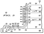
- FIG. 3 illustrates a greatly enlarged simplified sectional view of an optical waveguide module 101. It should be understood that similar feature and elements identified hereinabove will retain their original identifying numerals. Further, it should be understood that FIG. 3 is sectional view, thus the figure can extend into and out of the drawing.
- Optical waveguide module 101 includes of several elements or features, such as an interconnect substrate 129 having surface 130, a waveguide 103, a flexible substrate 51, photonic devices 111 and 112 with working portions 113 and 114, heat dissipating device 120, integrated circuit 125, interconnect substrate 129 having surface 130.
- Interconnect substrate 129 further includes an alignment device 148, bonding pad 149, and electrical trace 150.
- Waveguide 103 further includes surfaces 104 and 105, end surface 106, cladding regions 107 and core regions 108 and 109.
- Flexible substrate 51 also includes bonding pads 132-138 and corresponding conductive bumps 139-144.
- Interconnect substrate 129 is made of any suitable substrate, such as a printed circuit board, a FR4 board, a ceramic interconnect board, or the like. It should be understood that interconnect substrate 129 can be configured into a wide variety of forms that allow further integration of optical devices with standard electrical components. Generally, interconnect substrate 129 enables additional electrical coupling between flexible substrate 51 to interconnect substrate 129, thereby further integrating photonic devices 111 and 112 with standard electrical components. Electrical coupling between interconnect substrate 129 and flexible substrate 51 is achieved by any suitable method or technique, such as wire bonding, bump bonding, tape assisted bonding (TAB), or the like. For the sake of simplicity and for illustrative purposes only, interconnect substrate 129 is coupled with flexible substrate 51 by a wire bond 151, thereby electrically coupling bonding pad 149 with bonding pad 138.
- TAB tape assisted bonding
- Electrical trace 150 is illustrated as only a single electrical trace; however, it should be understood that electrical trace 150 can be a plurality of electrical traces that travel throughout interconnect substrate 129, thereby providing conductive paths for electrical signals to travel throughout flexible substrate 51, thus enabling electrical coupling of interconnect substrate 129 to a wide range of standard electronic components and systems.
- waveguide 103 as shown in FIG. 3 is fabricated in a similar manner as waveguide 10 shown in FIG. 1, wherein core regions 108 and 109 are surrounded by cladding region 107.
- waveguide 103 can also be made as having a single core region 108, as well as having a plurality of core region that are stacked on top or each other.
- FIG. 3 more clearly illustrates waveguide 103 in relation to other associated components of optical waveguide module 101.
- End surface 106 exposes a portion of core region 108, a portion of core region 109 and a portion of cladding region 107, thereby forming optical surfaces that light, indicated by arrows 115 and 116, can enter or leave waveguide 103.
- alignment device 117 is formed on end surface 106.
- Alignment device 117 is formed by an suitable method or technique, such as a tab, an alignment fiducial, an opening, or the like. Generally, alignment device 117 is used to align flexible substrate 51 to waveguide 103, thereby optically coupling windows 70 and 71 to core regions 105 and 106.
- thermally conductive traces 153, 154 and 155 illustrates a method to remove heat from photonic devices 111.
- Thermally conductive trace 153 and 154 are fabricated adjacent to a high heat concentration, thereby allowing thermally conductive trace 153 and 154 to carry the heat away from the high heat concentration to low heat concentration.
- thermally conductive traces 153 and 154 are made of any suitable heat conductive material that is either electrically conductive or electrically nonconductive.
- indium tin oxide is electrically nonconductive
- copper, tin/lead, palladium/nickel are both electrically conductive and heat conductive.
- thermally conductive traces 153 being coupled to bonding pad 138, the heat generated by photonic device 111 is carried away through thermally conductive traces 153 and 155 into interconnect substrate 129, thereby cooling photonic device 111 and improving performance of photonic devices 111.
- Photonic devices 111 and 112 can be any suitable photonic device or combination of photonic devices.
- photonic devices 111 and 112 are photo-transmitters, a photo-receivers, or a combination thereof made by any suitable method or technique.
- the photo-transmitters can be any suitable device, such as a vertical cavity surface emitting laser (VCSEL), light emitting diode (LED), or the like.
- VCSEL vertical cavity surface emitting laser
- LED light emitting diode
- photonic device 112 being an array of photo-receivers
- the photo-receivers can be any suitable photo-receiving device such as a photodiode, e.g., P-I-N photodiode, PN photodiode, or the like.
- photonic devices 111 and 112 can be a broad range of photo-active devices capable of transmitting and receiving.
- Heat dissipating device can be any suitable device, such as fins, heat sinks, heat dissipaters or the like that dissipates heat away from photonic devices 111 and 112.
- Heat dissipating device 120 typically are made of any suitable heat conductive material, such as a metal, e.g., aluminum, copper, gold, an alloy, e.g., aluminum/copper, silicon/aluminum, or the like, thereby enabling heat removal from photonic devices 111 and 112. By dissipating heat from photonic devices 111 and 112, photonic devices 111 and 112 have improved performance and long term reliability.
- Electrical coupling of photonic devices 111 and 112 and integrated circuit 125 to flexible substrate 51 is accomplished by any suitable method or technique, such as wire bonding, TAB bonding, bump bonding, or the like.
- bump bonding of photonic devices 111 and 112 and integrated circuit 125 is achieved by bump balls 139-142 and 143-144, respectively.
- bonding methods can be mixed, e.g., photonic device being bump bonded and integrated circuit being wire bonded, thus enabling the bonding method to be varied in accordance with specific applications.
- integrated circuit 125 of FIG. 3 shows only a single integrated circuit, it should be understood that integrated circuit 125 represents a wide variety of standard electronic components, such as capacitors, resistors, discrete devices, and hybrid devices that can be located on flexible substrate 51, thereby enabling electrical signals to be processed by a wide variety of electronic devices.
- Accurate placement or alignment of flexible substrate 51 to waveguide 103 and to interconnect substrate 129 is achieved by any suitable method or technique, such as mechanical, machine vision, or the like, as well as any combination thereof.
- Any suitable mechanical alignment method or technique such as locks and keys, tabs and openings, or the like can be used.
- alignment devices 117 and 148 represents by tabs and openings, engage openings and, thereby aligning flexible substrate 51 to both waveguide 103 and interconnect substrate 129.
- any other suitable alignment technique such as a robotically controlled system that uses machine vision, or the like can be used.
- the machine vision can be further augmented by placing alignment fiducials or alignment features on any necessary surface of waveguide 103 flexible substrate 51, and interconnect substrate 129, thereby enabling reference points or alignment fiducials to be superimposed so as to provide precise specific alignment.
- Use of several different alignment fiducials and procedures, such as optical targets, position orientation, and openings and tabs are capable of achieving accurate placement of flexible substrate 51 to waveguide 103.
- Affixing or attachment of flexible substrate 51 to waveguide 103 and to interconnect substrate 129 is achieved by any suitable method or technique, such as an adhesive, e.g., epoxy, polyimide, or any ultraviolet curable adhesive, or the like.
- flexible substrate 51 is positioned and affixed to waveguide 103 by a robotic arm or the like.
- waveguide 103 can be held either by a jig on a table or held by a robotic arm (not shown).
- An optically transparent epoxy is applied to end surface 106.
- Flexible substrate 51 subsequently is applied to waveguide 103 by a robotic arm. Placement of flexible substrate 51 is aligned to waveguide 103 by any one of several alignment fiducial systems previously described.
- alignment device 117 is formed on end surface 106 of waveguide 103. Alignment device 117 is then recognized by a machine vision system which orients an opening in flexible substrate 51 to alignment device 117 and places the opening over alignment device 117, thus affixing flexible substrate 51 to waveguide 103.
- flexible substrate 51 is aligned and attached to interconnect substrate 129, thereby affixing a portion of flexible substrate 51 to interconnect substrate 129.
- electrical interconnection or operably coupling flexible substrate 51 to interconnect substrate 129 can be achieved by any suitable method such as wire bonding, bump bonding, tab bonding, or the like.
- flexible substrate 51 is wire bonded from bonding pad 138 to bonding pad 149 through wire bond 151, thus electrically interconnecting interconnect substrate 129 with flexible substrate 51, thus operably coupling photonic devices 111 and 112 though flexible substrate 51 to interconnect substrate 129.
- FIG. 4 is another greatly enlarged simplified sectional view of an optical waveguide module 160. It should be understood that similar features and elements identified hereinabove will retain their original identifying numerals. So as to more clearly illustrate the present invention, it should be understood that dimensions and relative sizing shown in FIG. 4 have been relaxed. Further, it should be understood that FIG. 4 is sectional view, thus the figure can extend into and out of the drawing.
- optical waveguide module 160 has been described hereinabove; however, several additional elements are included in FIG. 4, a heat conducting trace 161 with mating surfaces 162, bonding pads 164 and 165, and a spacing body 170 with a curved surface 171. For the sake of simplicity, optical waveguide module 160 has be simplified.
- Interconnect substrate 129 has been described hereinabove, with reference to FIG. 3, thus not necessitating a detailed description here.
- heat conducting trace 161 is joined with heat dissipating device 120 with mating surfaces 162, thereby providing a heat conduction path from photonic device 111 into interconnect substrate 129, thereby improving performance and life time of photonic device 111.
- Mating surfaces 162 are made of portions of conducting trace 161 and heat dissipating device 120 in any suitable configuration, such as flat surfaces, tabs and openings, or the like, thereby providing a good mechanical and heat conducting joint or union.
- Spacing body 170 provides a smooth transition from waveguide 103 to interconnect substrate 129 for flexible substrate 51, thereby reducing stress of flexible substrate 51 along curved surface 171.
- Spacing body 170 is made of any suitable plastic material, such as plastics, epoxies, polyimides, polyvinyl, or the like, thereby generating a smooth hard plastic material for flexible substrate 51 to transition to interconnect substrate 129.
- spacing body 170 is formed by any suitable method, such as molding, milling, or the like. However in a preferred embodiment of the present invention, spacing body 170 is made by molding an epoxy material.
- spacing body 170 is sized the same as waveguide 103, thereby enabling waveguide 103 and spacing body 170 to be joined.
- heat conducting device 120 is made of any suitable material, e.g., aluminum, copper, tin, or the like, as well as any suitable alloy, e.g., aluminum/copper, steel, or the like.
- Heat conductive device 120 is shaped to contact photonic device 111 and heat conducting trace 161.
- heat conduction device 120 is shaped with a flat surface that is mechanically affixed to photonic device 111 and to conducting trace 160. Affixing of heat conduction device 120 is achieved through any suitable method or technique, such as heat conductive epoxies, solder paste, press fitting, or the like.
- FIG. 5 is a simplified partially exploded pictorial illustration of an optoelectronic module 180. It should be understood that elements or features previously described in FIGs. 1-4 will retain their original identifying numerals.
- Optoelectronic module 180 is made of several elements or features, such as interconnect substrate 129, waveguide 103 having a plurality of core regions 31 and 32, alignment ferrules 27, photonic devices 111 and 112, flexible substrate 51, integrated circuit 125, an integrated circuit 181, and plastic portions 184. Additionally, an optical connector 185 having an optical cable 186, body 187, and an alignment guide 188 is illustrated.
- waveguide 103 is operably coupled to photonic devices 111 and 112 through flexible substrate 51.
- Photonic devices 111 and 112 are illustrated as an array spanning the plurality of core regions 31 and 32.
- the array can be of any suitable configuration.
- the array can be made of individual photonic devices that are assembled or the array can be made an entire unit. Devices incorporated into the array can be photo-transmitters, photo-receivers, or any combination thereof.
- Photonic devices 111 and 112 is mounted to flexible substrate 51 so that working portions of photonic devices 111 and 112 are aligned to individual core regions of the plurality of core regions 31 and 32, thus providing maximum light transmission through waveguide 103.
- waveguide 103 is attached to interconnect substrate 129 by any suitable method or technique such as adhering, press fitting, molding, or the like.
- an epoxy adhesive is applied to interconnect substrate 129 at an appropriate location where waveguide 103 and interconnect substrate 129 are to be bonded.
- Waveguide 103 is subsequently placed into the adhesive by an automated system such as a robot arm (not shown), thereby providing accurate placement and orientation of waveguide 103.
- Electrical coupling of standard electronic components, illustrated by integrated circuit 125, to flexible substrate 51 is achieved by any suitable method or technique, such as wire bonding, bump bonding, TAB, or the like. It should be understood that specific selection of electrical coupling is application specific.
- plastic encapsulation of interconnect substrate 129, waveguide 103, flexible substrate 51 is achieved by an overmolding process, represented by plastic portions 184.
- Plastic portions 184 encapsulate the above mentioned elements while leaving alignment ferrules 27 and the plurality of core regions 31 and 32 open and clear of debris.
- optical surfaces form optical cable 62 can be mated and aligned to the plurality of core regions 31 and 32 in waveguide 103.
- the optoelectronic mount enables the incorporation of standard electronic components and optical components such that advantages of the optical components can be utilized. Further it should be noted that the method and article of the present invention allow this integration in a cost effective manner by providing a way of eliminating costly steps carried out by hand and to automate the remaining manufacturing steps thus making the entire process highly manufacturable.
Landscapes
- Physics & Mathematics (AREA)
- General Physics & Mathematics (AREA)
- Optics & Photonics (AREA)
- Engineering & Computer Science (AREA)
- Microelectronics & Electronic Packaging (AREA)
- Condensed Matter Physics & Semiconductors (AREA)
- Electromagnetism (AREA)
- Optical Integrated Circuits (AREA)
- Optical Couplings Of Light Guides (AREA)
- Semiconductor Lasers (AREA)
Applications Claiming Priority (2)
| Application Number | Priority Date | Filing Date | Title |
|---|---|---|---|
| US08/456,207 US5539848A (en) | 1995-05-31 | 1995-05-31 | Optical waveguide module and method of making |
| US456207 | 1995-05-31 |
Publications (3)
| Publication Number | Publication Date |
|---|---|
| EP0745873A2 true EP0745873A2 (de) | 1996-12-04 |
| EP0745873A3 EP0745873A3 (de) | 1997-02-05 |
| EP0745873B1 EP0745873B1 (de) | 1999-09-22 |
Family
ID=23811892
Family Applications (1)
| Application Number | Title | Priority Date | Filing Date |
|---|---|---|---|
| EP96108454A Expired - Lifetime EP0745873B1 (de) | 1995-05-31 | 1996-05-28 | Optisches Wellenleitermodul und Verfahren zu seiner Herstellung |
Country Status (6)
| Country | Link |
|---|---|
| US (1) | US5539848A (de) |
| EP (1) | EP0745873B1 (de) |
| JP (1) | JPH08327843A (de) |
| KR (1) | KR960042107A (de) |
| DE (1) | DE69604333T2 (de) |
| GR (1) | GR3032135T3 (de) |
Cited By (3)
| Publication number | Priority date | Publication date | Assignee | Title |
|---|---|---|---|---|
| EP1686404A3 (de) * | 2005-02-01 | 2006-08-23 | Ibiden Co., Ltd. | Optisches Transmitter-Empfänger Modul, Verfahren zur Herstellung dieses Moduls und Datenkommunikationssystem, das ein solches Modul enthält |
| US11071199B2 (en) | 2018-10-09 | 2021-07-20 | City University Of Hong Kong | Optical printed circuit board and its fabrication method |
| US11899255B2 (en) | 2022-06-17 | 2024-02-13 | City University Of Hong Kong | Optical printed circuit board and its fabricating method |
Families Citing this family (63)
| Publication number | Priority date | Publication date | Assignee | Title |
|---|---|---|---|---|
| CA2161915A1 (en) * | 1994-11-02 | 1996-05-03 | Sosaku Sawada | Optical module circuit board having flexible structure |
| NL9500328A (nl) * | 1995-02-21 | 1996-10-01 | Framatome Connectors Belgium | Werkwijze voor het vervaardigen van een connector voor optische geleiders op een printkaart, alsmede beschermingskap en positioneringsstuk voor toepassing bij deze werkwijze. |
| US6805493B2 (en) | 1996-03-12 | 2004-10-19 | 3M Innovative Properties Company | Optical connector assembly using partial large diameter alignment features |
| US5940562A (en) * | 1996-03-12 | 1999-08-17 | Minnesota Mining And Manufacturing Company | Stubless optoelectronic device receptacle |
| US5790733A (en) * | 1996-06-07 | 1998-08-04 | Minnesota Mining And Manufactouring Company | Optoelectronic device receptacle and method of making same |
| US5774614A (en) * | 1996-07-16 | 1998-06-30 | Gilliland; Patrick B. | Optoelectronic coupling and method of making same |
| US5636298A (en) * | 1996-08-19 | 1997-06-03 | Motorola | Coalescing optical module and method for making |
| AU4602597A (en) * | 1996-09-30 | 1998-04-24 | Whitaker Corporation, The | Fiber optic array transmitter/receiver based on flexible circuit technology |
| DE69710098T2 (de) | 1996-12-31 | 2002-08-29 | Honeywell, Inc. | Flexible optische verbindungseinheit |
| EP0893861A3 (de) * | 1997-07-25 | 2000-01-12 | Oki Electric Industry Co., Ltd. | Optischer Modul |
| US5913002A (en) * | 1997-12-31 | 1999-06-15 | The Whitaker Corporation | Optical coupling device for passive alignment of optoelectronic devices and fibers |
| US6317189B1 (en) | 1998-12-29 | 2001-11-13 | Xerox Corporation | High-efficiency reflective liquid crystal display |
| US6588949B1 (en) * | 1998-12-30 | 2003-07-08 | Honeywell Inc. | Method and apparatus for hermetically sealing photonic devices |
| US7004644B1 (en) | 1999-06-29 | 2006-02-28 | Finisar Corporation | Hermetic chip-scale package for photonic devices |
| US6485192B1 (en) * | 1999-10-15 | 2002-11-26 | Tyco Electronics Corporation | Optical device having an integral array interface |
| US6792178B1 (en) | 2000-01-12 | 2004-09-14 | Finisar Corporation | Fiber optic header with integrated power monitor |
| US7169355B1 (en) * | 2000-02-02 | 2007-01-30 | Applera Corporation | Apparatus and method for ejecting sample well trays |
| US6396968B2 (en) * | 2000-03-02 | 2002-05-28 | Siemens Aktiengesellschaft | Optical signal transmission device |
| US6879014B2 (en) * | 2000-03-20 | 2005-04-12 | Aegis Semiconductor, Inc. | Semitransparent optical detector including a polycrystalline layer and method of making |
| US6670599B2 (en) | 2000-03-27 | 2003-12-30 | Aegis Semiconductor, Inc. | Semitransparent optical detector on a flexible substrate and method of making |
| WO2001073902A2 (en) * | 2000-03-31 | 2001-10-04 | Aegis Semiconductor | An optical communication device including a semitransparent optical detector |
| US6547454B2 (en) | 2000-09-21 | 2003-04-15 | Corona Optical Systems, Inc. | Method to align optical components to a substrate and other optical components |
| US6450704B1 (en) * | 2000-10-05 | 2002-09-17 | Corona Optical Systems, Inc. | Transparent substrate and hinged optical assembly |
| US6867377B2 (en) | 2000-12-26 | 2005-03-15 | Emcore Corporation | Apparatus and method of using flexible printed circuit board in optical transceiver device |
| US7021836B2 (en) * | 2000-12-26 | 2006-04-04 | Emcore Corporation | Attenuator and conditioner |
| US6863444B2 (en) | 2000-12-26 | 2005-03-08 | Emcore Corporation | Housing and mounting structure |
| US6799902B2 (en) | 2000-12-26 | 2004-10-05 | Emcore Corporation | Optoelectronic mounting structure |
| US6905260B2 (en) | 2000-12-26 | 2005-06-14 | Emcore Corporation | Method and apparatus for coupling optical elements to optoelectronic devices for manufacturing optical transceiver modules |
| US20020122637A1 (en) * | 2000-12-26 | 2002-09-05 | Anderson Gene R. | Optical transmitter, receiver or transceiver module |
| CN100354699C (zh) * | 2001-08-02 | 2007-12-12 | 伊吉斯半导体公司 | 可调谐光学仪器 |
| US7439449B1 (en) | 2002-02-14 | 2008-10-21 | Finisar Corporation | Flexible circuit for establishing electrical connectivity with optical subassembly |
| US7446261B2 (en) | 2001-09-06 | 2008-11-04 | Finisar Corporation | Flexible circuit boards with tooling cutouts for optoelectronic modules |
| US6617518B2 (en) * | 2001-11-02 | 2003-09-09 | Jds Uniphase Corporaton | Enhanced flex cable |
| US20030085452A1 (en) * | 2001-11-05 | 2003-05-08 | International Business Machines Corporation | Packaging architecture for a multiple array transceiver using a continuous flexible circuit |
| FR2836235B1 (fr) * | 2002-02-21 | 2004-07-02 | Framatome Connectors Int | Ferule de connexion de fibres optiques |
| US7044657B2 (en) * | 2002-03-19 | 2006-05-16 | Finisar Corporation | Transistor outline package with exteriorly mounted resistors |
| US7254149B2 (en) | 2002-03-19 | 2007-08-07 | Finisar Corporation | Submount, pedestal, and bond wire assembly for a transistor outline package with reduced bond wire inductance |
| US7042067B2 (en) * | 2002-03-19 | 2006-05-09 | Finisar Corporation | Transmission line with integrated connection pads for circuit elements |
| US6932518B2 (en) * | 2002-03-19 | 2005-08-23 | Finisar Corporation | Circuit board having traces with distinct transmission impedances |
| US7532782B2 (en) * | 2002-04-18 | 2009-05-12 | Pivotal Decisions Llc | Flexible optical circuit apparatus and method |
| US7526207B2 (en) * | 2002-10-18 | 2009-04-28 | Finisar Corporation | Flexible circuit design for improved laser bias connections to optical subassemblies |
| US6863453B2 (en) | 2003-01-28 | 2005-03-08 | Emcore Corporation | Method and apparatus for parallel optical transceiver module assembly |
| US6807346B2 (en) * | 2003-03-01 | 2004-10-19 | Optovia Corporation | Method for attaching multiple light sources to an optoelectronic module |
| GB2401196B (en) * | 2003-05-02 | 2007-02-07 | Agilent Technologies Inc | Packaged planar lightwave circuit arrangements corresponding method of connection and component |
| JP2007524828A (ja) * | 2003-06-20 | 2007-08-30 | アイギス セミコンダクター インコーポレイテッド | 熱光学フィルタ及びそれを用いた赤外線センサ |
| US20050018994A1 (en) * | 2003-07-24 | 2005-01-27 | Oepic, Inc. | Active and passive to-can extension boards |
| US7128472B2 (en) * | 2003-07-31 | 2006-10-31 | International Business Machines Corporation | Method and apparatus for providing optoelectronic communication with an electronic device |
| JP2007503622A (ja) * | 2003-08-26 | 2007-02-22 | レッドシフト システムズ コーポレイション | 赤外線カメラシステム |
| US7221827B2 (en) * | 2003-09-08 | 2007-05-22 | Aegis Semiconductor, Inc. | Tunable dispersion compensator |
| WO2005036240A1 (en) * | 2003-10-07 | 2005-04-21 | Aegis Semiconductor, Inc. | Tunable optical filter with heater on a cte-matched transparent substrate |
| US7275937B2 (en) | 2004-04-30 | 2007-10-02 | Finisar Corporation | Optoelectronic module with components mounted on a flexible circuit |
| US7311240B2 (en) | 2004-04-30 | 2007-12-25 | Finisar Corporation | Electrical circuits with button plated contacts and assembly methods |
| US7425135B2 (en) * | 2004-04-30 | 2008-09-16 | Finisar Corporation | Flex circuit assembly |
| US7629537B2 (en) * | 2004-07-09 | 2009-12-08 | Finisar Corporation | Single layer flex circuit |
| JP2006030294A (ja) * | 2004-07-12 | 2006-02-02 | Nitto Denko Corp | フレキシブル光導波路の製法 |
| JP4704125B2 (ja) * | 2005-06-22 | 2011-06-15 | 浜松ホトニクス株式会社 | 光デバイス |
| GB2434971B (en) * | 2006-02-14 | 2011-03-02 | Ronald Alexander Young | Squeegee device |
| JP4850148B2 (ja) * | 2007-08-23 | 2012-01-11 | 独立行政法人産業技術総合研究所 | 光モジュール |
| JP2012013916A (ja) * | 2010-06-30 | 2012-01-19 | Hitachi Cable Ltd | 光学部品および光モジュール |
| JP5920128B2 (ja) * | 2012-09-07 | 2016-05-18 | 住友電気工業株式会社 | 光導波路型受光素子の製造方法および光導波路型受光素子 |
| US9101083B2 (en) | 2012-09-10 | 2015-08-04 | Apple Inc. | T-flex bonder |
| EP3671297B1 (de) * | 2018-12-21 | 2025-02-26 | Adtran Networks SE | Elektrooptische anordnung |
| JP7138056B2 (ja) * | 2019-01-24 | 2022-09-15 | 京セラ株式会社 | 光コネクタモジュール及び光導波路基板の製造方法 |
Family Cites Families (9)
| Publication number | Priority date | Publication date | Assignee | Title |
|---|---|---|---|---|
| JPS5720601A (en) * | 1980-07-14 | 1982-02-03 | Hitachi Ltd | Control rod driving mechanism for nuclear reactor |
| JPS6126002A (ja) * | 1984-07-17 | 1986-02-05 | Hoya Corp | 集光性屈折率分布型ロツドレンズアレ−の製造法 |
| EP0420173A3 (en) * | 1989-09-26 | 1992-09-09 | Omron Corporation | Rib optical waveguide and method of manufacturing the same |
| US5265184A (en) * | 1992-05-28 | 1993-11-23 | Motorola, Inc. | Molded waveguide and method for making same |
| US5271083A (en) * | 1992-07-27 | 1993-12-14 | Motorola, Inc. | Molded optical waveguide with contacts utilizing leadframes and method of making same |
| US5249245A (en) * | 1992-08-31 | 1993-09-28 | Motorola, Inc. | Optoelectroinc mount including flexible substrate and method for making same |
| US5325451A (en) * | 1993-01-05 | 1994-06-28 | Motorola, Inc. | Modular optical waveguide and method for making |
| EP0616234B1 (de) * | 1993-03-18 | 1999-06-02 | Nippon Telegraph And Telephone Corporation | Herstellungsverfahren von optischen Wellenleitern aus Polyimid |
| US5367593A (en) * | 1993-09-03 | 1994-11-22 | Motorola, Inc. | Optical/electrical connector and method of fabrication |
-
1995
- 1995-05-31 US US08/456,207 patent/US5539848A/en not_active Expired - Fee Related
-
1996
- 1996-05-17 JP JP8146485A patent/JPH08327843A/ja active Pending
- 1996-05-23 KR KR1019960018110A patent/KR960042107A/ko not_active Ceased
- 1996-05-28 DE DE69604333T patent/DE69604333T2/de not_active Expired - Fee Related
- 1996-05-28 EP EP96108454A patent/EP0745873B1/de not_active Expired - Lifetime
-
1999
- 1999-12-15 GR GR990403220T patent/GR3032135T3/el unknown
Cited By (7)
| Publication number | Priority date | Publication date | Assignee | Title |
|---|---|---|---|---|
| EP1686404A3 (de) * | 2005-02-01 | 2006-08-23 | Ibiden Co., Ltd. | Optisches Transmitter-Empfänger Modul, Verfahren zur Herstellung dieses Moduls und Datenkommunikationssystem, das ein solches Modul enthält |
| US7338218B2 (en) | 2005-02-01 | 2008-03-04 | Ibiden Co., Ltd. | Optical module, method of manufacturing the optical module, and data communication system including the optical module |
| US7551812B2 (en) | 2005-02-01 | 2009-06-23 | Ibiden Co., Ltd. | Optical module, method of manufacturing the optical module, and data communication system including the optical module |
| US7674049B2 (en) | 2005-02-01 | 2010-03-09 | Ibiden Co., Ltd. | Optical module, method of manufacturing the optical module, and data communication system including the optical module |
| EP2053436A3 (de) * | 2005-02-01 | 2013-01-23 | Ibiden Co., Ltd. | Optisches Modul mit einem flexiblen Kabel |
| US11071199B2 (en) | 2018-10-09 | 2021-07-20 | City University Of Hong Kong | Optical printed circuit board and its fabrication method |
| US11899255B2 (en) | 2022-06-17 | 2024-02-13 | City University Of Hong Kong | Optical printed circuit board and its fabricating method |
Also Published As
| Publication number | Publication date |
|---|---|
| EP0745873A3 (de) | 1997-02-05 |
| DE69604333T2 (de) | 2000-04-13 |
| KR960042107A (ko) | 1996-12-21 |
| JPH08327843A (ja) | 1996-12-13 |
| EP0745873B1 (de) | 1999-09-22 |
| US5539848A (en) | 1996-07-23 |
| DE69604333D1 (de) | 1999-10-28 |
| GR3032135T3 (en) | 2000-04-27 |
Similar Documents
| Publication | Publication Date | Title |
|---|---|---|
| US5539848A (en) | Optical waveguide module and method of making | |
| US5625734A (en) | Optoelectronic interconnect device and method of making | |
| US5249245A (en) | Optoelectroinc mount including flexible substrate and method for making same | |
| US5521992A (en) | Molded optical interconnect | |
| US5768456A (en) | Optoelectronic package including photonic device mounted in flexible substrate | |
| US5482658A (en) | Method of making an optoelectronic interface module | |
| EP0618468B1 (de) | Eine Schnittstelle zum Koppeln von optischen Fasern mit elektronischen Schaltungen | |
| US5416870A (en) | Optoelectronic interface device and method with reflective surface | |
| US6935792B2 (en) | Optoelectronic package and fabrication method | |
| US5309537A (en) | Optoelectronic coupling device and method of making | |
| EP1028341B1 (de) | Integriertes Verpackungssystem für optische Übertragungseinrichtungen, das die automatische Ausrichtung mit optischen Fasern erlaubt | |
| US5337398A (en) | Single in-line optical package | |
| EP0529947B1 (de) | Optische Baugruppe zur Justierung eines aktiven optischen Bauelements und einer optischen Faser und Verfahren zur Herstellung der Baugruppe | |
| US5452387A (en) | Coaxial optoelectronic mount and method of making same | |
| US20060215969A1 (en) | Optical semiconductor module and its manufacturing method | |
| US20020154869A1 (en) | Multi-functional fiber optic coupler | |
| JP2001281505A (ja) | 光電子装置およびその製造方法 | |
| US5275970A (en) | Method of forming bonding bumps by punching a metal ribbon | |
| US5539200A (en) | Integrated optoelectronic substrate | |
| EP1477832A1 (de) | Optisches Modul mit einem optoelektronischen Bauteil, das in einem Loch eines Substrats montiert ist. | |
| US8698264B2 (en) | Photoelectric conversion module | |
| KR100945621B1 (ko) | 광 통신 모듈 및 그 제조 방법 | |
| US6762119B2 (en) | Method of preventing solder wetting in an optical device using diffusion of Cr | |
| US5384873A (en) | Optical interface unit and method of making | |
| US5500914A (en) | Optical interconnect unit and method or making |
Legal Events
| Date | Code | Title | Description |
|---|---|---|---|
| PUAI | Public reference made under article 153(3) epc to a published international application that has entered the european phase |
Free format text: ORIGINAL CODE: 0009012 |
|
| AK | Designated contracting states |
Kind code of ref document: A2 Designated state(s): DE FR GB GR SE |
|
| PUAL | Search report despatched |
Free format text: ORIGINAL CODE: 0009013 |
|
| AK | Designated contracting states |
Kind code of ref document: A3 Designated state(s): DE FR GB GR SE |
|
| 17P | Request for examination filed |
Effective date: 19970805 |
|
| 17Q | First examination report despatched |
Effective date: 19971007 |
|
| GRAG | Despatch of communication of intention to grant |
Free format text: ORIGINAL CODE: EPIDOS AGRA |
|
| GRAG | Despatch of communication of intention to grant |
Free format text: ORIGINAL CODE: EPIDOS AGRA |
|
| GRAG | Despatch of communication of intention to grant |
Free format text: ORIGINAL CODE: EPIDOS AGRA |
|
| GRAH | Despatch of communication of intention to grant a patent |
Free format text: ORIGINAL CODE: EPIDOS IGRA |
|
| GRAH | Despatch of communication of intention to grant a patent |
Free format text: ORIGINAL CODE: EPIDOS IGRA |
|
| GRAA | (expected) grant |
Free format text: ORIGINAL CODE: 0009210 |
|
| AK | Designated contracting states |
Kind code of ref document: B1 Designated state(s): DE FR GB GR SE |
|
| REF | Corresponds to: |
Ref document number: 69604333 Country of ref document: DE Date of ref document: 19991028 |
|
| ET | Fr: translation filed | ||
| PLBE | No opposition filed within time limit |
Free format text: ORIGINAL CODE: 0009261 |
|
| STAA | Information on the status of an ep patent application or granted ep patent |
Free format text: STATUS: NO OPPOSITION FILED WITHIN TIME LIMIT |
|
| 26N | No opposition filed | ||
| REG | Reference to a national code |
Ref country code: GB Ref legal event code: IF02 |
|
| PGFP | Annual fee paid to national office [announced via postgrant information from national office to epo] |
Ref country code: FR Payment date: 20050517 Year of fee payment: 10 |
|
| PGFP | Annual fee paid to national office [announced via postgrant information from national office to epo] |
Ref country code: GR Payment date: 20060406 Year of fee payment: 11 Ref country code: GB Payment date: 20060406 Year of fee payment: 11 |
|
| PGFP | Annual fee paid to national office [announced via postgrant information from national office to epo] |
Ref country code: SE Payment date: 20060504 Year of fee payment: 11 |
|
| PGFP | Annual fee paid to national office [announced via postgrant information from national office to epo] |
Ref country code: DE Payment date: 20060531 Year of fee payment: 11 |
|
| EUG | Se: european patent has lapsed | ||
| GBPC | Gb: european patent ceased through non-payment of renewal fee |
Effective date: 20070528 |
|
| REG | Reference to a national code |
Ref country code: FR Ref legal event code: ST Effective date: 20080131 |
|
| PG25 | Lapsed in a contracting state [announced via postgrant information from national office to epo] |
Ref country code: DE Free format text: LAPSE BECAUSE OF NON-PAYMENT OF DUE FEES Effective date: 20071201 |
|
| PG25 | Lapsed in a contracting state [announced via postgrant information from national office to epo] |
Ref country code: GB Free format text: LAPSE BECAUSE OF NON-PAYMENT OF DUE FEES Effective date: 20070528 |
|
| PG25 | Lapsed in a contracting state [announced via postgrant information from national office to epo] |
Ref country code: SE Free format text: LAPSE BECAUSE OF NON-PAYMENT OF DUE FEES Effective date: 20070529 |
|
| PG25 | Lapsed in a contracting state [announced via postgrant information from national office to epo] |
Ref country code: FR Free format text: LAPSE BECAUSE OF NON-PAYMENT OF DUE FEES Effective date: 20070531 |
|
| PG25 | Lapsed in a contracting state [announced via postgrant information from national office to epo] |
Ref country code: FR Free format text: LAPSE BECAUSE OF NON-PAYMENT OF DUE FEES Effective date: 20060531 |
|
| PG25 | Lapsed in a contracting state [announced via postgrant information from national office to epo] |
Ref country code: GR Free format text: LAPSE BECAUSE OF NON-PAYMENT OF DUE FEES Effective date: 20071204 |