EP0745923A2 - Régulation de tension avec stabilisation du pÔle de la charge - Google Patents
Régulation de tension avec stabilisation du pÔle de la charge Download PDFInfo
- Publication number
- EP0745923A2 EP0745923A2 EP96303017A EP96303017A EP0745923A2 EP 0745923 A2 EP0745923 A2 EP 0745923A2 EP 96303017 A EP96303017 A EP 96303017A EP 96303017 A EP96303017 A EP 96303017A EP 0745923 A2 EP0745923 A2 EP 0745923A2
- Authority
- EP
- European Patent Office
- Prior art keywords
- output
- voltage
- stage
- input
- current
- Prior art date
- Legal status (The legal status is an assumption and is not a legal conclusion. Google has not performed a legal analysis and makes no representation as to the accuracy of the status listed.)
- Granted
Links
Images
Classifications
-
- G—PHYSICS
- G05—CONTROLLING; REGULATING
- G05F—SYSTEMS FOR REGULATING ELECTRIC OR MAGNETIC VARIABLES
- G05F3/00—Non-retroactive systems for regulating electric variables by using an uncontrolled element, or an uncontrolled combination of elements, such element or such combination having self-regulating properties
- G05F3/02—Regulating voltage or current
- G05F3/08—Regulating voltage or current wherein the variable is DC
- G05F3/10—Regulating voltage or current wherein the variable is DC using uncontrolled devices with non-linear characteristics
- G05F3/16—Regulating voltage or current wherein the variable is DC using uncontrolled devices with non-linear characteristics being semiconductor devices
- G05F3/20—Regulating voltage or current wherein the variable is DC using uncontrolled devices with non-linear characteristics being semiconductor devices using diode- transistor combinations
- G05F3/26—Current mirrors
- G05F3/267—Current mirrors using both bipolar and field-effect technology
Definitions
- This invention relates to electronic circuits used as voltage regulators and more specifically to circuits and methods used to stabilize a voltage regulator.
- Voltage regulators are inherently medium to high gain circuits, typically 50db or greater, with low bandwidth. With this high gain and low bandwidth, stability is often achieved by setting a dominate pole with the load capacitor. Achieving stability over a wide range of load currents with a low value load capacitor (-O.luF) is difficult because the load pole formed by the load capacitor and load resistor can vary by more than three decades of frequency and be as high as tens of KHz requiring the circuit to have a very broad band of greater than 3MHz which is incompatible with the power process used for voltage regulators.
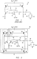
- FIG. 1 shows a prior art solution to the stabilization problem.
- the voltage regulator 24 in Fig. 1 converts an unregulated Vdd voltage, 12 volts in this example, into a regulated voltage at node 26, 5 volts in this example.
- Capacitor 8, resistor 10, amplifier 12, and resistor 14 are configured as an integrator having the output voltage node 26 as an inverting input and a voltage reference as the non-inverting input.
- the integrator drives bipolar transistor 4 which is connected in series with an output current mirror formed by p-channel transistors 2 and 16, as is known in the art.
- Resistor 18 is a pull down resistor added to increase the stability of the circuit.
- the invention can be summarized as a voltage regulator with load pole stabilization.
- the voltage regulator consists of an output stage, a comparator stage, and an active load.
- the active load draws current from the output of the voltage regulator inversely proportional to the current demand on the voltage regulator. When the output current demand is large, the active load draws relatively low current. When the output current demand is large, the active load draws a relatively large amount of current. Consequently, the disclosed voltage regulator has high stability without consuming excess power.
- Fig. 1 is a schematic diagram of a voltage regulator with a pull down resistor as is known in the prior art.
- Fig. 2 is a schematic diagram of a voltage regulator with an active load.
- the voltage regulator 60 comprises a comparator stage 62, an output stage 64, and an active load 66.
- the comparator stage 62 is constructed by connecting a base of a NPN transistor to a first plate of capacitor 44 and to an output of an operational amplifier 46.
- the emitter of transistor 40 is connected an emitter of a NPN transistor 36 and to a draining end of a current source 42.
- the sourcing end of the current source is connected to a voltage reference, ground.
- the base of transistor 36 is connected to a bias voltage which is not shown.
- the second plate of capacitor 44 is connected to a first end of resistor 45.
- the second end of resistor 45 is connected to an inverting input of amplifier 46 and to the first end of resistor 48.
- the non-inverting input is connected to a reference voltage, which is this example is 5 volts.
- the regulator will track the reference voltage, as is understood in the art.
- the output stage is constructed by connecting a drain and a gate of P-channel transistor 38 and a gate of a P-channel transistor 50 to the collector of transistor 40. This connection comprises the output of the comparator stage and the input of the output stage.
- the sources of transistors 38 and 50 are connected to a Vdd, which in this example is 12 volts.
- the drain of transistor 50 is connected to the second end of resistor 48 and to a drain of N-channel transistor 54. This connection forms the output of the output stage, the output of the voltage regulator, and the input of the comparator stage.
- the active load 66 is constructed by connecting the collector of transistor 36 to the drain and the gate of a P-channel transistor 34 transistor and to the gate of a P-channel transistor 30.
- the sources of transistors 30 and 34 are connected Vdd.
- the drain of transistor 30 is connected to the drain and gate of N-channel transistor 32 and to the gate of an N-channel transistor 54.
- the sources of transistors 32 and 54 are connected to ground.
- the load which is not part of the invention is shown as a resistor 56 connected in parallel with a capacitor 58.
- the current mirror created by transistor 38 being connected to transistor 50 comprise the output stage.
- the output stage drives current onto node 52 responsive to a comparator stage.
- the current flowing through transistor 50 is proportional to the current flowing through transistor 38 where the proportion is determined by the relative areas of the transistors as is known in the art.
- the resulting voltage on node 52 is sensed through resistor 48 and compared to the voltage reference on the non-inverting input of amplifier 46.
- the integrator formed by capacitor 44 and resistor 45 create the dominate pole and has a zero that cancels the load pole.
- the output of amplifier 46 drives transistor 40 which drives the current through the current mirror of the output stage.
- the current through transistor 40 is limited by the current source 42.
- Transistor 36, transistor 40 and current source 42 are configured as a differential pair. Therefore, the current through transistors 36 and 40 equals the current of current source 42. As the current demand on the output stage increases, current through transistor 40 increases and current through transistor 36 decreases by a proportional amount. Conversely, as the current through transistor 40 decreases, the current through transistor 36 increases by a proportional amount.
- the current through transistor 36 is mirrored through the current mirror created by transistors 30 and 34.
- the current through transistor 30 is mirrored by the current mirror created by transistor 32 and transistor 54. Consequently, the active load 66 current increases as the current through output stage 64 decreases; conversely, if the current through the output stage 64 increases, the current through the active load 54 decreases.
- the voltage regulator 60 provides the advantage of increasing the stability of voltage regulator 60 without increasing the power dissipated in the circuit. Additionally, voltage regulator 60 has an active pull down resistor which decreases in resistance when necessary to maintain stability and increases resistance to decrease power consumption when the extra load is not needed for stability.
Landscapes
- Engineering & Computer Science (AREA)
- Physics & Mathematics (AREA)
- Microelectronics & Electronic Packaging (AREA)
- Nonlinear Science (AREA)
- Electromagnetism (AREA)
- General Physics & Mathematics (AREA)
- Radar, Positioning & Navigation (AREA)
- Automation & Control Theory (AREA)
- Continuous-Control Power Sources That Use Transistors (AREA)
- Control Of Electrical Variables (AREA)
- Amplifiers (AREA)
Applications Claiming Priority (2)
| Application Number | Priority Date | Filing Date | Title |
|---|---|---|---|
| US08/456,120 US5637992A (en) | 1995-05-31 | 1995-05-31 | Voltage regulator with load pole stabilization |
| US456120 | 1995-05-31 |
Publications (3)
| Publication Number | Publication Date |
|---|---|
| EP0745923A2 true EP0745923A2 (fr) | 1996-12-04 |
| EP0745923A3 EP0745923A3 (fr) | 1997-07-16 |
| EP0745923B1 EP0745923B1 (fr) | 2005-08-03 |
Family
ID=23811510
Family Applications (1)
| Application Number | Title | Priority Date | Filing Date |
|---|---|---|---|
| EP96303017A Expired - Lifetime EP0745923B1 (fr) | 1995-05-31 | 1996-04-30 | Régulation de tension avec stabilisation du pôle de la charge |
Country Status (4)
| Country | Link |
|---|---|
| US (1) | US5637992A (fr) |
| EP (1) | EP0745923B1 (fr) |
| JP (1) | JPH08328671A (fr) |
| DE (1) | DE69635008D1 (fr) |
Cited By (4)
| Publication number | Priority date | Publication date | Assignee | Title |
|---|---|---|---|---|
| EP0862102A1 (fr) * | 1997-02-28 | 1998-09-02 | STMicroelectronics, Inc. | Régulateur de tension stabilisé par le pÔle de la charge |
| US5852359A (en) * | 1995-09-29 | 1998-12-22 | Stmicroelectronics, Inc. | Voltage regulator with load pole stabilization |
| EP0851332A3 (fr) * | 1996-12-19 | 1999-03-24 | Texas Instruments Incorporated | Régulateur de tension |
| EP0957421A3 (fr) * | 1998-05-13 | 2000-03-15 | Texas Instruments Incorporated | Régulateur de tension, efficace en courant, à faible tension de déchet avec une régualtion de la charge et une réponse en fréquence améliorée |
Families Citing this family (18)
| Publication number | Priority date | Publication date | Assignee | Title |
|---|---|---|---|---|
| FR2751488B1 (fr) * | 1996-07-16 | 1998-10-16 | Sgs Thomson Microelectronics | Amplificateur de puissance en technologie bicmos a etage de sortie en technologie mos |
| GB9721908D0 (en) * | 1997-10-17 | 1997-12-17 | Philips Electronics Nv | Voltage regulator circuits and semiconductor circuit devices |
| US5973540A (en) * | 1998-01-23 | 1999-10-26 | National Semiconductor Corporation | Ladder tracking buffer amplifier |
| JP3315652B2 (ja) * | 1998-09-07 | 2002-08-19 | キヤノン株式会社 | 電流出力回路 |
| US6359425B1 (en) * | 1999-12-13 | 2002-03-19 | Zilog, Inc. | Current regulator with low voltage detection capability |
| US6246555B1 (en) * | 2000-09-06 | 2001-06-12 | Prominenet Communications Inc. | Transient current and voltage protection of a voltage regulator |
| US6333623B1 (en) | 2000-10-30 | 2001-12-25 | Texas Instruments Incorporated | Complementary follower output stage circuitry and method for low dropout voltage regulator |
| ATE490498T1 (de) * | 2002-07-16 | 2010-12-15 | Dsp Group Switzerland Ag | Kapazitive rückführungsschaltung |
| US6879142B2 (en) * | 2003-08-20 | 2005-04-12 | Broadcom Corporation | Power management unit for use in portable applications |
| US7026802B2 (en) * | 2003-12-23 | 2006-04-11 | Cypress Semiconductor Corporation | Replica biased voltage regulator |
| US7298567B2 (en) | 2004-02-27 | 2007-11-20 | Hitachi Global Storage Technologies Netherlands B.V. | Efficient low dropout linear regulator |
| US6960907B2 (en) * | 2004-02-27 | 2005-11-01 | Hitachi Global Storage Technologies Netherlands, B.V. | Efficient low dropout linear regulator |
| US7205828B2 (en) * | 2004-08-02 | 2007-04-17 | Silicon Laboratories, Inc. | Voltage regulator having a compensated load conductance |
| US7262586B1 (en) | 2005-03-31 | 2007-08-28 | Cypress Semiconductor Corporation | Shunt type voltage regulator |
| US7859240B1 (en) | 2007-05-22 | 2010-12-28 | Cypress Semiconductor Corporation | Circuit and method for preventing reverse current flow into a voltage regulator from an output thereof |
| US20110309808A1 (en) | 2010-06-16 | 2011-12-22 | Aeroflex Colorado Springs Inc. | Bias-starving circuit with precision monitoring loop for voltage regulators with enhanced stability |
| EP2952996B1 (fr) * | 2014-06-02 | 2019-03-13 | Dialog Semiconductor (UK) Limited | Étage de collecteur de courant pour LDO |
| EP3951551B1 (fr) * | 2020-08-07 | 2023-02-22 | Scalinx | Régulateur de tension et procédé |
Family Cites Families (8)
| Publication number | Priority date | Publication date | Assignee | Title |
|---|---|---|---|---|
| US4628247A (en) * | 1985-08-05 | 1986-12-09 | Sgs Semiconductor Corporation | Voltage regulator |
| US5519309A (en) * | 1988-05-24 | 1996-05-21 | Dallas Semiconductor Corporation | Voltage to current converter with extended dynamic range |
| US4943737A (en) * | 1989-10-13 | 1990-07-24 | Advanced Micro Devices, Inc. | BICMOS regulator which controls MOS transistor current |
| US5053640A (en) * | 1989-10-25 | 1991-10-01 | Silicon General, Inc. | Bandgap voltage reference circuit |
| DE59010535D1 (de) * | 1990-12-22 | 1996-11-14 | Itt Ind Gmbh Deutsche | Spannungsregler mit einem CMOS-Transkonduktanzverstärker mit gleitendem Arbeitspunkt |
| US5182526A (en) * | 1991-07-18 | 1993-01-26 | Linear Technology Corporation | Differential input amplifier stage with frequency compensation |
| DE4233850C1 (de) * | 1992-10-08 | 1994-06-23 | Itt Ind Gmbh Deutsche | Schaltungsanordnung zur Stromeinstellung eines monolithisch integrierten Padtreibers |
| US5512816A (en) * | 1995-03-03 | 1996-04-30 | Exar Corporation | Low-voltage cascaded current mirror circuit with improved power supply rejection and method therefor |
-
1995
- 1995-05-31 US US08/456,120 patent/US5637992A/en not_active Expired - Lifetime
-
1996
- 1996-04-30 DE DE69635008T patent/DE69635008D1/de not_active Expired - Lifetime
- 1996-04-30 EP EP96303017A patent/EP0745923B1/fr not_active Expired - Lifetime
- 1996-05-16 JP JP8121986A patent/JPH08328671A/ja active Pending
Cited By (7)
| Publication number | Priority date | Publication date | Assignee | Title |
|---|---|---|---|---|
| US5852359A (en) * | 1995-09-29 | 1998-12-22 | Stmicroelectronics, Inc. | Voltage regulator with load pole stabilization |
| EP0851332A3 (fr) * | 1996-12-19 | 1999-03-24 | Texas Instruments Incorporated | Régulateur de tension |
| EP0862102A1 (fr) * | 1997-02-28 | 1998-09-02 | STMicroelectronics, Inc. | Régulateur de tension stabilisé par le pÔle de la charge |
| US5850139A (en) * | 1997-02-28 | 1998-12-15 | Stmicroelectronics, Inc. | Load pole stabilized voltage regulator circuit |
| US5945818A (en) * | 1997-02-28 | 1999-08-31 | Stmicroelectronics, Inc. | Load pole stabilized voltage regulator circuit |
| EP0890895A3 (fr) * | 1997-07-08 | 1999-04-14 | STMicroelectronics, Inc. | Régulation de tension avec stabilisation du pÔle de la charge |
| EP0957421A3 (fr) * | 1998-05-13 | 2000-03-15 | Texas Instruments Incorporated | Régulateur de tension, efficace en courant, à faible tension de déchet avec une régualtion de la charge et une réponse en fréquence améliorée |
Also Published As
| Publication number | Publication date |
|---|---|
| EP0745923A3 (fr) | 1997-07-16 |
| US5637992A (en) | 1997-06-10 |
| DE69635008D1 (de) | 2005-09-08 |
| JPH08328671A (ja) | 1996-12-13 |
| EP0745923B1 (fr) | 2005-08-03 |
Similar Documents
| Publication | Publication Date | Title |
|---|---|---|
| EP0745923A2 (fr) | Régulation de tension avec stabilisation du pÔle de la charge | |
| EP0766164B1 (fr) | Régulateur de tension avec stabilisation du pôle de la charge | |
| US6157176A (en) | Low power consumption linear voltage regulator having a fast response with respect to the load transients | |
| EP0862102A1 (fr) | Régulateur de tension stabilisé par le pÔle de la charge | |
| US5646518A (en) | PTAT current source | |
| US6956727B1 (en) | High side current monitor with extended voltage range | |
| US5939867A (en) | Low consumption linear voltage regulator with high supply line rejection | |
| US7443149B2 (en) | Regulator circuit capable of detecting variations in voltage | |
| EP0735452A2 (fr) | Circuit limiteur de courant | |
| US20090167263A1 (en) | Current limiting circuit and voltage regulator using the same | |
| US4808907A (en) | Current regulator and method | |
| KR950010341A (ko) | 온도 변화에 대해 일정하게 유지되는 출력 신호 진폭을 갖는 ic | |
| US6249162B1 (en) | Hysteresis circuit | |
| EP0946911B1 (fr) | CIRCUIT INVERSEUR POLARISE DE FAçON A LIMITER LE COURANT D'ATTAQUE MAXIMUM DESTINE A UN ETAGE SUIVANT, ET PROCEDE CORRESPONDANT | |
| US4556805A (en) | Comparator circuit having hysteresis voltage substantially independent of variation in power supply voltage | |
| EP0008897A1 (fr) | Source de tension constante | |
| US4325019A (en) | Current stabilizer | |
| US20050206362A1 (en) | Low-voltage bandgap reference circuit | |
| KR920009548B1 (ko) | 전류원 장치 | |
| US20060097709A1 (en) | Linear voltage regulator | |
| US6175265B1 (en) | Current supply circuit and bias voltage circuit | |
| KR0167562B1 (ko) | 전류 임계 검출기 회로 | |
| US6621333B1 (en) | Circuit and method to counter offset voltage induced by load changes | |
| JPH0413692Y2 (fr) | ||
| SU1130842A2 (ru) | Стабилизатор посто нного напр жени |
Legal Events
| Date | Code | Title | Description |
|---|---|---|---|
| PUAI | Public reference made under article 153(3) epc to a published international application that has entered the european phase |
Free format text: ORIGINAL CODE: 0009012 |
|
| AK | Designated contracting states |
Kind code of ref document: A2 Designated state(s): DE FR GB IT |
|
| PUAL | Search report despatched |
Free format text: ORIGINAL CODE: 0009013 |
|
| AK | Designated contracting states |
Kind code of ref document: A3 Designated state(s): DE FR GB IT |
|
| 17P | Request for examination filed |
Effective date: 19980105 |
|
| 17Q | First examination report despatched |
Effective date: 19980205 |
|
| RAP3 | Party data changed (applicant data changed or rights of an application transferred) |
Owner name: STMICROELECTRONICS, INC. |
|
| GRAP | Despatch of communication of intention to grant a patent |
Free format text: ORIGINAL CODE: EPIDOSNIGR1 |
|
| GRAS | Grant fee paid |
Free format text: ORIGINAL CODE: EPIDOSNIGR3 |
|
| GRAA | (expected) grant |
Free format text: ORIGINAL CODE: 0009210 |
|
| AK | Designated contracting states |
Kind code of ref document: B1 Designated state(s): DE FR GB IT |
|
| PG25 | Lapsed in a contracting state [announced via postgrant information from national office to epo] |
Ref country code: IT Free format text: LAPSE BECAUSE OF FAILURE TO SUBMIT A TRANSLATION OF THE DESCRIPTION OR TO PAY THE FEE WITHIN THE PRE;WARNING: LAPSES OF ITALIAN PATENTS WITH EFFECTIVE DATE BEFORE 2007 MAY HAVE OCCURRED AT ANY TIME BEFORE 2007. THE CORRECT EFFECTIVE DATE MAY BE DIFFERENT FROM THE ONE RECORDED.SCRIBED TIME-LIMIT Effective date: 20050803 |
|
| REG | Reference to a national code |
Ref country code: GB Ref legal event code: FG4D |
|
| REF | Corresponds to: |
Ref document number: 69635008 Country of ref document: DE Date of ref document: 20050908 Kind code of ref document: P |
|
| PG25 | Lapsed in a contracting state [announced via postgrant information from national office to epo] |
Ref country code: DE Free format text: LAPSE BECAUSE OF FAILURE TO SUBMIT A TRANSLATION OF THE DESCRIPTION OR TO PAY THE FEE WITHIN THE PRESCRIBED TIME-LIMIT Effective date: 20051104 |
|
| ET | Fr: translation filed | ||
| PLBE | No opposition filed within time limit |
Free format text: ORIGINAL CODE: 0009261 |
|
| STAA | Information on the status of an ep patent application or granted ep patent |
Free format text: STATUS: NO OPPOSITION FILED WITHIN TIME LIMIT |
|
| 26N | No opposition filed |
Effective date: 20060504 |
|
| REG | Reference to a national code |
Ref country code: FR Ref legal event code: PLFP Year of fee payment: 20 |
|
| PGFP | Annual fee paid to national office [announced via postgrant information from national office to epo] |
Ref country code: FR Payment date: 20150319 Year of fee payment: 20 Ref country code: GB Payment date: 20150324 Year of fee payment: 20 |
|
| REG | Reference to a national code |
Ref country code: GB Ref legal event code: PE20 Expiry date: 20160429 |
|
| PG25 | Lapsed in a contracting state [announced via postgrant information from national office to epo] |
Ref country code: GB Free format text: LAPSE BECAUSE OF EXPIRATION OF PROTECTION Effective date: 20160429 |