EP0745941B1 - System und Verfahren zur Bereitstellung einer flexiblen Speicherhierarchie - Google Patents
System und Verfahren zur Bereitstellung einer flexiblen Speicherhierarchie Download PDFInfo
- Publication number
- EP0745941B1 EP0745941B1 EP96303792A EP96303792A EP0745941B1 EP 0745941 B1 EP0745941 B1 EP 0745941B1 EP 96303792 A EP96303792 A EP 96303792A EP 96303792 A EP96303792 A EP 96303792A EP 0745941 B1 EP0745941 B1 EP 0745941B1
- Authority
- EP
- European Patent Office
- Prior art keywords
- memory
- data
- sub
- memory element
- blocks
- Prior art date
- Legal status (The legal status is an assumption and is not a legal conclusion. Google has not performed a legal analysis and makes no representation as to the accuracy of the status listed.)
- Expired - Lifetime
Links
Images
Classifications
-
- G—PHYSICS
- G06—COMPUTING OR CALCULATING; COUNTING
- G06F—ELECTRIC DIGITAL DATA PROCESSING
- G06F12/00—Accessing, addressing or allocating within memory systems or architectures
- G06F12/02—Addressing or allocation; Relocation
- G06F12/08—Addressing or allocation; Relocation in hierarchically structured memory systems, e.g. virtual memory systems
-
- G—PHYSICS
- G06—COMPUTING OR CALCULATING; COUNTING
- G06F—ELECTRIC DIGITAL DATA PROCESSING
- G06F12/00—Accessing, addressing or allocating within memory systems or architectures
- G06F12/02—Addressing or allocation; Relocation
- G06F12/08—Addressing or allocation; Relocation in hierarchically structured memory systems, e.g. virtual memory systems
- G06F12/0802—Addressing of a memory level in which the access to the desired data or data block requires associative addressing means, e.g. caches
- G06F12/0893—Caches characterised by their organisation or structure
- G06F12/0897—Caches characterised by their organisation or structure with two or more cache hierarchy levels
Definitions
- the present invention relates to a computer system and method for providing a flexible memory hierarchy including a dedicated memory transfer bus, controlled by an operating system, for exchanging data between different memory types.
- a conventional computer system comprises a central processing unit (“CPU") and a memory system.
- the CPU fetches data of an arbitrary bit length (e.g., blocks) from physical (or real memory) address locations within the memory system. Since the CPU normally operates at a greater speed than the memory system, the overall performance of the computer system is significantly influenced by the rate at which data may be accessed from memory (“bandwidth”) and the time delay experienced by the CPU before it obtains access to such data (“memory latency").
- the memory system is arranged according to a strict, inflexible hierarchy.
- This hierarchy typically features multiple memory types, each of these memory types having a predetermined, unique physical (or real memory) address space. Examples of these memory types include low-speed main memory (e.g., dynamic random access memory “DRAM”, video random access memory “VRAM”, etc.), high-speed cache memory (typically being a multiple-level cache having a bandwidth greater than the low-speed memory), and remote memory (disk storage devices, main memory of another computer system, etc.) being “slower” (i.e., having a lesser bandwidth) than both cache and main memory.
- “high-speed” memory has a bandwidth of approximately 12 nanoseconds while low speed memory and remotely located memories have a bandwidth of approximately 50 nanoseconds and 300 microseconds, respectively.
- the most-recently-used data is stored in the high-speed cache memory and lesser used data is stored in the other slower memory types.
- pre-configured hardware e.g., a CPU controller
- this method of prediction may not be varied by the computer operator nor by the operating system of the computer system, both of which would be more accurate predictors than the CPU controller.
- the computer operator would have knowledge as to which data will be more frequently accessed by an application program.
- US-A-5,386,547 discloses a simple mixed first level cache memory system which includes a level 1 cache connected to a processor by read data and write data lines.
- the level 1 cache is connected to level 2 cache by swap tag lines, swap data lines, a multiplexer and a swap/read line.
- the level 2 cache is connected to the next lower level in the memory hierarchy by a write tag and write data lines.
- the next lower level in the memory hierarchy below the level 2 cache is also connected by a read data line through the multiplexer and the swap/read line to the level 1 cache.
- the instruction or data is present in the level 1 cache, it is supplied to the processor on the read data line. If the instruction or data is not present in the level 1 cache, the processor looks for it in the level 2 cache by putting out the address of the instruction or data on the instruction or data address lines. If the instruction or data is in the level 2 cache, it is supplied to the processor through the level 1 cache by means of a swap operation on the tag swap lines, the swap data lines, the multiplexer and the swap/read data line. If the instruction or data is present in neither the level 1 cache nor the level 2 cache, the address on the instruction or data address lines fetches the instruction or data from successively lower levels in the memory hierarchy as required via the read data line, the multiplexer and the swap/read data line. The instruction or data is then supplied from the level 1 cache to the processor.
- a central processing unit has a cache memory system associated therewith for interfacing with a main memory system.
- the cache memory system includes a primary cache comprised of SRAMS and a secondary cache comprised of DRAM.
- the primary cache has a faster access than the secondary cache.
- the secondary cache indicates a hit
- data is accessed from the appropriate one of the arrays and transferred through the primary cache via transfer circuits to the data bus. Simultaneously therewith, the data is stored in an appropriate one of the arrays.
- a hit does not occur in either the secondary cache or the primary cache
- data is retrieved from the main system memory through a buffer/multiplexer circuit on one side of the secondary cache and passed through both the secondary cache and the primary cache and stored therein in a single operation due to the line for line transfer provided by the transfer circuits.
- the present invention describes a system and method for providing a flexible memory hierarchy utilizing a memory transfer bus which, under the control of programmable operating system software, is dedicated to transferring data between different memory types.
- the description describes the transfer of data between high-speed and low-speed memories sharing a single real memory address space since transfers between these memories and remote-memories occurs in the same fashion.
- a “node” is defined as one or more hardware components used to perform a given operation.
- “data” may include binary data and/or instructions, both of which are generically referred to as “data” unless otherwise distinguished.
- a "page” is defined as a plurality of sub-blocks each of which includes at least one byte of data and status information (e.g., a status bit) to indicate whether the byte(s) of data stored within the sub-block are "valid” or "invalid".
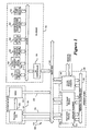
- the computer system 100 comprises a first bus 110, preferably a central processing unit (“CPU") bus, including data, address control bus lines preferably configured with bit widths of 128, 32 and 8 bits respectively. It is contemplated, however, that these above-listed bus lines may be configured with any bit width.
- the first bus 110 allows information (i.e., data, address and/or control) to be communicated between a plurality of nodes including, but not limited to, a processor node 120, a memory node 130 and an input/output ("I/O") node 150.
- I/O input/output
- the processor node 120 includes at least one processing unit 121 and a memory management unit ("MMU") 122. Although only one processing unit 121 is illustrated in this embodiment, it is contemplated that multiple processing units could be employed herein.
- the processing unit 121 is coupled to the first bus 110 through a pair of unidirectional signal lines 123 and 124, which collectively enable the processing unit 121 to receive information from and transfer information to the memory node 130.
- the processing unit 121 is further coupled to the MMU 122 via communication lines 125 so that the processing unit 121 can transfer a virtual address to the MMU 122 which, in turn, translates the virtual address into a real memory address.
- Such translation is accomplished through translation tables provided by operating system software. These translation tables include a high-speed memory translation table and a low-speed translation table for converting a particular virtual address into its corresponding real memory address utilized by the high-speed and low-speed memories, respectively.
- the MMU 122 coupled to the first bus 110 via unidirectional signal line 126, places the real memory address corresponding to the virtual address and necessary control information onto the first bus 110 to be read by the memory node 130.
- the control information may include, but is not limited to, operation type, bus grant, bus ownership and sharing modes such as MOESI, MESI, etc.
- the I/O node 150 includes an I/O controller 155 which operates as an interface between the first bus 110 and a conventional I/O bus 160. This provides a communication path (i.e., gateway) to allow nodes coupled to the first bus 110 and the I/O bus 160 to exchange information.
- I/O controller 155 operates as an interface between the first bus 110 and a conventional I/O bus 160. This provides a communication path (i.e., gateway) to allow nodes coupled to the first bus 110 and the I/O bus 160 to exchange information.
- the I/O bus 160 communicates information to at least one peripheral device in the computer system 100 including, but not limited to a display device 161 (e.g., cathode ray tube, liquid crystal display, flat panel display, etc.) for displaying images; an alphanumeric input device 162 (e.g., an alphanumeric keyboard, etc.) for communicating information and command selections to the processing unit 121; a cursor control device 163 (e.g., a mouse, trackball, touch pad, joystick, etc.) for controlling cursor movement; a mass storage device 164 (e.g., magnetic tapes, hard disk drive, floppy disk drive, etc.) for storing data; an information transceiver device 165 (fax machine, modem, scanner etc.) for transmitting information from the computer system 100 to another system and for receiving information from another system; and a hard copy device 166 (e.g., plotter, printer, etc.) for providing a tangible, visual representation of the information. It is contemplated that the computer
- the memory node 130 includes a memory element 135 storing data associated with the real memory address and a remote memory controller 140, similar to a CPU controller, which controls a transmission of a single sub-block of data (e.g., a single cache line being 32-bytes in size) between the computer system 100 and a remote system.
- the memory element 135 is page-mapped memory organized into a plurality of pages wherein each page has a plurality of consecutive memory addresses.
- the memory element 135 is populated with high-speed memory 136 (e.g., static random access memory) and low-speed memory 137 (e.g., dynamic random access memory "DRAM", video random access memory "VRAM” and the like).
- the memory element 135 is scalable in that bandwidth of the memory element 135 may be increased and memory latency reduced by populating it with a greater proportion of high-speed memory 136.
- the memory element 135 and the remote memory controller 140 are coupled to a dedicated memory transfer bus 145 having an arbitrary-chosen bit width. This bit width is chosen for optimal data transfer and thus, may vary from the bit width of the first bus 110.
- the memory transfer bus 145 primarily supports data transfers between the high-speed and low-speed memories 136 and 137. These data transfers are initiated by the processing unit 121 and controlled by the operating system software through the processing unit. These data transfers typically are “bulk” memory transfers in increments of a "page” of data at a time. Contrary to conventional memory hierarchies, data transfers through the dedicated memory transfer bus 145 may occur without substantial effect on the latency bandwidth of the first bus 110.
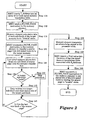
- a data transfer from low-speed memory to high-speed memory through the dedicated memory transfer bus begins with Step 105 by the processor node, namely the MMU, inserting a targeted real memory page address ("T_Address") into an available entry of a high-speed memory translation table.
- T_Address is the address of the high-speed memory targeted to receive a page of data during the data transfer (hereinafter referred to as "target memory”). This is done so that any subsequent memory "read” or "write” instructions to the virtual address corresponding to the T_Address are directed to the high-speed memory.
- the MMU transmits a FLUSH_PAGE instruction to the memory element which causes the memory element to set or assert the status bits of each sub-block of the target memory to indicate that these sub-blocks contain "invalid" data (Step 115).
- the performance of this instruction enables data to be written to the target memory and stalls any memory "read” requests transmitted to the target memory prior to clearing or deasserting the status bits to reflect the presence of "valid" data.
- the MMU transmits an instruction ("MOVE_PAGE") to the memory element to move a page of data beginning at a source page address "S_Address" (hereinafter referred to as a "source page") from the low-speed memory to target memory.
- MOVE_PAGE an instruction
- the low-speed memory sequentially places the data from each sub-block of the source page onto the memory transfer bus (Step 125).
- the memory system determines whether a first sub-block of the target memory (i.e., "first targeted sub-block”), being the destination of the first sub-block placed on the memory transfer bus, is "valid" (Step 130).
- This determination is performed to check whether in case the processing unit wrote data to the first targeted sub-block after the FLUSH_PAGE instruction but before the MOVE_PAGE instruction because the operations on the memory transfer bus are independent of the first bus operations. If the first targeted sub-block is "valid”, the memory system is configured to discard the data associated with the first sub-block (Step 135) and check whether the first sub-block is the last sub-block of the source page (Step 145). However, if the targeted sub-block is "invalid", the data within the first sub-block is written into the first targeted sub-block and the status bit of the first targeted sub-block is cleared indicating that valid data resides therein (Step 140). The data transfer procedure continues until the data associated with the last sub-block of the source page is transferred (Step 145).
- the memory element transmits an acknowledge signal ("MOVE_FINISH") to the MMU (Step 150).
- the MOVE_FINISH signal causes the MMU to insert a "Null" value into an entry of a low-speed memory translation table previously containing the S_Address (Step 155). By inserting the Null value, the entry is cleared to allow the operating system to reuse the entry and the memory corresponding to that entry.
- the MMU transmits a FLUSH_PAGE instruction to the low-speed memory in order to set those sub-blocks used to store the source page to "invalid" state (Step 160).
- the memory transfer bus supports data transfers from high-speed memory to low-speed memory.
- the operating system software which primarily governs virtual-to-real mapping, inserts T_Address into an available entry of the low-speed memory translation table and inserts a Null value into an entry associated with the high-speed memory translation table at S_Address (Steps 205-210).
- the processor node has no control over the data transfers from high-speed to the low-speed memory since such data transfers are not immediately required by the processing unit.
- the MMU transmits a MOVE_PAGE instruction to the memory element to request the memory element to transfer a source page beginning at S_Address in the high-speed memory into the low-speed memory at T_Address (Step 215). Thereafter, upon completion of the data transfer utilizing the memory transfer bus as described above in Steps 125-145, with the exception that the data transfer is from high-speed to low-speed memory, the memory element returns a MOVE_FINISH signal acknowledging that the data transfer has been completed (Steps 220-225). This prompts the MMU to transmit the FLUSH_PAGE instruction to the memory element in order to set status bits of the sub-blocks associated with the source page at S_Address to an "invalid" state (Step 230).
- the processing unit 121 frequently requires data stored in the memory element 135.
- the processor node 120 In order to obtain such data, the processor node 120 typically produces the memory "read" request. Since data transfers between different memory types along the dedicated memory transfer bus 145 may occur during the memory read request, it is necessary to provide a procedure which supports both operations concurrently.
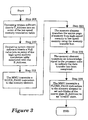
- Step 305 the processing unit initiates a memory "read” instruction (Step 305) and thereafter, transfers the memory "read” instruction for data stored within a particular virtual address into the MMU (Step 310). If the MMU determines that the virtual address is not included in the high-speed memory translation table, normally maintained by operating system software, the MMU maps the virtual address into a real low-speed memory address according to the low-speed memory translation table (Steps 315-320).
- the MMU issues a memory read request by placing the real low-speed memory address along with any necessary control information including operation type, bus grant, bus ownership, sharing modes such as MOESI, MESI, etc. onto the first bus for servicing by the memory element (Step 325).
- the memory element services the memory read request by placing the requested data onto the first bus to be subsequently read by the processing unit (Steps 330-335).
- the MMU determines that the virtual address is included in the high-speed memory translation table
- the MMU maps the virtual address into a real high-speed memory address according to the high-speed memory translation table (Step 340).
- the MMU issues a memory read request by placing this real high-speed memory address along with any control information onto the first bus for servicing by the memory element (Step 345).
- the memory element determines whether the data at the real memory address is "valid" (Step 350). This is done to prevent accessing data which is invalid because, for example, an outstanding data transfer has not yet completed prior to the memory read request. If valid, the memory element services the memory read request by placing the requested data onto the data bus to be subsequently read by the processing unit (Steps 330-335). Otherwise, if the data is invalid, the memory element waits for the data transfer to complete and the data is validated. The address remains in the memory system buffers until the data is available. Memory address requests are buffered in the memory system.
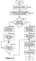
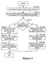
- the processing unit initiates a memory write instruction (Step 405) and thereafter, transfers the memory write instruction for data stored within a particular virtual address into the MMU (Step 410). If the MMU determines that the virtual address is not included in the high-speed memory translation table, the MMU maps the virtual address into a low-speed real memory address according to the low-speed memory translation table (Step 415-420).
- the MMU issues a memory write request by placing the low-speed real memory address along with any necessary control information onto the first bus for servicing by the memory element as the processor places the data onto the first bus to be written into the slow-speed memory of the memory element (Step 425-430).
- the MMU determines that the virtual address is included in the high-speed memory translation table
- the MMU maps the virtual address into a real high-speed memory address according to the high speed translation table (Steps 415, 435).
- the MMU issues a memory write request by placing the real high-speed memory address along with any control information onto the first bus for servicing by the memory element (Step 440).
- the data is written into the sub-block and the status bit associated with the sub-block is cleared to indicate that the data is "valid" (Step 445).
- data transfers between the memory element and a remote system via the memory transfer bus follow the same procedures as discussed in Figures 2 and 3 with a few exceptions.
- the remote system may only read "copy blocks" having read-only access from the memory element of the computer system; however, the computer system can read a single block (e.g., one cache line) of data from the remote system and write a single block of data from the remote system into the memory element.
- a second exception is that it is not possible for the remote system to write data to another remote system without permission being granted by the operating system of the computer system. This can be circumvented, however, through additional status information.
Landscapes
- Engineering & Computer Science (AREA)
- Theoretical Computer Science (AREA)
- Physics & Mathematics (AREA)
- General Engineering & Computer Science (AREA)
- General Physics & Mathematics (AREA)
- Memory System Of A Hierarchy Structure (AREA)
Claims (12)
- Computersystem, das Folgendes umfasst:einen Prozessorknoten (120) zum Verarbeiten von Informationen;einen Speicherknoten (130) zum Speichern der genannten Informationen, wobei der Speicherknoten (130) ein seitenweise abgebildeter Speicher ist und ein erstes Speicherelement (136) und ein zweites Speicherelement (137) umfasst, wobei das erste Speicherelement (136) so konfiguriert ist, dass es eine größere Bandbreite unterstützt als das zweite Speicherelement (137) und das erste und das zweite Speicherelement (136, 137) einen einzigen realen Speicheradressraum gemeinsam nutzen;einen ersten Bus (110), der mit dem Prozessorknoten (120) und dem Speicherknoten (130) verbunden ist, damit die genannten Informationen zwischen dem Prozessorknoten (120) und dem Speicherknoten (130) übertragen werden können; undeinen zweiten Speichertransferbus (145), der unabhängig von dem genannten ersten Bus (110) arbeitet, wobei der Speichertransferbus (145) mit dem ersten und dem zweiten Speicherelement (136, 137) verbunden ist und es ermöglicht, dass eine Seite von im ersten Speicherelement (136) gespeicherten Daten zum zweiten Speicherelement (137) übertragen und dort gespeichert wird, und eine Seite von im zweiten Speicherelement (137) gespeicherten Daten zum ersten Speicherelement (136) übertragen und dort gespeichert wird; dadurch gekennzeichnet, dass jede Seite eine Mehrzahl von Subblöcken oder Cache-Speicherleitungen beinhaltet, von denen jede(r) wenigstens ein Byte Daten und Statusinformationen enthält, die angeben, ob die Daten gültig sind.
- Computersystem nach Anspruch 1, bei dem das erste Speicherelement (136) ein statischer Arbeitsspeicher ist, der eine Mehrzahl von Subblöcken mit Daten und Statusinformationen speichert.
- Computersystem nach Anspruch 2, bei dem das zweite Speicherelement (137) ein dynamischer Arbeitsspeicher ist, der eine Mehrzahl von Subblöcken mit Daten und Statusinformationen speichert.
- Computersystem nach Anspruch 1, 2 oder 3, bei dem die Übertragung der genannten Seite von Daten durch den Speichertransferbus (145), der unabhängig vom ersten Bus (110) arbeitet, durch Betriebssystemsoftware gesteuert wird.
- Computersystem nach Anspruch 1, 2, 3 oder 4, ferner umfassend eine Speicherfernsteuerung (140), die es ermöglicht, dass die genannte Seite von Daten zwischen dem Speicherknoten (130) und einem ortsfern befindlichen Peripherieknoten übertragen wird.
- Verfahren zum Übertragen einer Seite mit einer Mehrzahl von Subblöcken oder Cache-Speicherleitungen, von denen jede(r) wenigstens ein Byte Daten und Statusinformationen enthält, die angeben, ob die Daten gültig sind, zwischen einem ersten Speicherelement und einem zweiten Speicherelement (137) durch einen dedizierten Speichertransferbus (145), wobei das erste Speicherelement (136) so konfiguriert wird, dass es eine größere Bandbreite unterstützt als das zweite Speicherelement (137), wobei das Verfahren die folgenden Schritte umfasst:Empfangen einer Anweisung zum Übertragen einer Seite von Daten mit einer Mehrzahl von Subblöcken im ersten Speicherelement (136) vom ersten Speicherelement (136) zum zweiten Speicherelement (137), wobei die genannten ersten und zweiten Speicherelemente (136, 137) einen einzelnen realen Speicheradressraum gemeinsam nutzen;sequentielles Übertragen der Seite von Daten vom ersten Speicherelement (136) auf den dedizierten Speichertransferbus (145);Schreiben von Daten, die sich in jedem aus der Mehrzahl von Subblöcken befinden, in einen entsprechenden angestrebten Subblock einer Mehrzahl von angestrebten Subblöcken des genannten ersten Speicherelementes (136), vorausgesetzt, die entsprechenden Subblöcke sind in einem "ungültigen" Zustand; undEinstellen von Statusinformationen der Mehrzahl von Subblöcken so, dass sie anzeigen, dass sich die Daten der Mehrzahl von Subblöcken in einem "ungültigen" Zustand befinden.
- Verfahren nach Anspruch 6, wobei das Verfahren vor dem Empfangsschritt die Schritte des Einfügens einer Zieladresse in einen Eintrag einer Hochgeschwindigkeits-Speicherumsetztabelle umfasst; und
Setzen von Statusbits der Mehrzahl von angestrebten Subblöcken des zweiten Speicherelementes (137) in einen "ungültig" Status, um es zuzulassen, dass die Seite von Daten in die Mehrzahl von angestrebten Subblöcken geschrieben wird. - Verfahren nach Anspruch 7, bei dem der sequentielle Übertragungsschritt die folgenden Schritte umfasst:Ausgeben von Daten, die mit einem aus der Mehrzahl von Subblöcken assoziiert sind, auf den dedizierten Speichertransferbus (145);Ausbreiten der Daten über den dedizierten Speichertransferbus (145); undErmitteln, ob ein Statusbit des angestrebten Subblocks einen "gültig" Zustand repräsentiert, wobeider angestrebte Subblock übersprungen wird, wenn der Subblock "gültig" ist; undder Schreibschritt durchgeführt wird, wenn der Subblock "ungültig" ist.
- Verfahren nach Anspruch 6, wobei das Verfahren vor dem Setzschritt ferner einen Schritt des Sendens eines Steuersignals vom ersten Speicherelement (136) zu einem Prozessorknoten (120) beinhaltet, um anzuzeigen, dass die Seite von Daten über den dedizierten Speichertransferbus (145) übertragen wurde.
- Verfahren nach Anspruch 9, wobei das Verfahren nach dem Schritt des Sendens des Steuersignals vom ersten Speicherelement (136) zu einem Prozessorknoten (120) ferner den Schritt des Einfügens eines Null-Wertes in einen Eintrag einer Niedergeschwindigkeits-Speicherumsetztabelle beinhaltet, die mit der Mehrzahl von Subblöcken assoziiert ist.
- Verfahren nach Anspruch 6, wobei das Verfahren vor dem Empfangsschritt die folgenden Schritte umfasst:Einfügen einer Zieladresse in einen Eintrag einer Niedergeschwindigkeits-Speicherumsetztabelle durch Betriebssystemsoftware, wobei der genannte Eintrag die Mehrzahl von angestrebten Subblöcken repräsentiert; undEinfügen eines Null-Wertes in einen Eintrag einer Hochgeschwindigkeits-Speicherumsetztabelle, die die Mehrzahl von Subblöcken repräsentiert.
- Verfahren nach Anspruch 11, wobei das Verfahren vor dem Setzschritt ferner den Schritt das Sendens eines Signals vom ersten Speicherelement (136) zu einem Prozessorknoten (120) beinhaltet, um anzuzeigen, dass die Seite von Daten über einen dedizierten Speichertransferbus (145) übertragen wurde.
Applications Claiming Priority (2)
| Application Number | Priority Date | Filing Date | Title |
|---|---|---|---|
| US46018895A | 1995-06-02 | 1995-06-02 | |
| US460188 | 1995-06-02 |
Publications (3)
| Publication Number | Publication Date |
|---|---|
| EP0745941A2 EP0745941A2 (de) | 1996-12-04 |
| EP0745941A3 EP0745941A3 (de) | 1997-02-26 |
| EP0745941B1 true EP0745941B1 (de) | 2003-08-06 |
Family
ID=23827707
Family Applications (1)
| Application Number | Title | Priority Date | Filing Date |
|---|---|---|---|
| EP96303792A Expired - Lifetime EP0745941B1 (de) | 1995-06-02 | 1996-05-28 | System und Verfahren zur Bereitstellung einer flexiblen Speicherhierarchie |
Country Status (4)
| Country | Link |
|---|---|
| US (2) | US5812816A (de) |
| EP (1) | EP0745941B1 (de) |
| JP (1) | JPH09179779A (de) |
| DE (1) | DE69629331T2 (de) |
Families Citing this family (12)
| Publication number | Priority date | Publication date | Assignee | Title |
|---|---|---|---|---|
| DE69629331T2 (de) * | 1995-06-02 | 2004-02-12 | Sun Microsystems, Inc., Mountain View | System und Verfahren zur Bereitstellung einer flexiblen Speicherhierarchie |
| US6032271A (en) * | 1996-06-05 | 2000-02-29 | Compaq Computer Corporation | Method and apparatus for identifying faulty devices in a computer system |
| DE69817192D1 (de) | 1997-09-05 | 2003-09-18 | Sun Microsystems Inc | Mehrprozessorrechnersystem mit verwendung eines gruppenschutzmechanismus |
| US6553475B2 (en) * | 1997-10-09 | 2003-04-22 | Matsushita Electric Industrial Co., Ltd. | Memory system with address conversion based on inherent performance condition |
| US6665749B1 (en) * | 1999-08-17 | 2003-12-16 | Nec Electronics, Inc. | Bus protocol for efficiently transferring vector data |
| US6665787B2 (en) * | 2000-02-29 | 2003-12-16 | International Business Machines Corporation | Very high speed page operations in indirect accessed memory systems |
| US7523290B2 (en) * | 2000-02-29 | 2009-04-21 | International Business Machines Corporation | Very high speed page operations in indirect accessed memory systems |
| US7782363B2 (en) * | 2000-06-27 | 2010-08-24 | Front Row Technologies, Llc | Providing multiple video perspectives of activities through a data network to a remote multimedia server for selective display by remote viewing audiences |
| JP2003108438A (ja) * | 2001-09-28 | 2003-04-11 | Supreme Magic:Kk | データ処理装置 |
| US6681301B1 (en) | 2001-10-02 | 2004-01-20 | Advanced Micro Devices, Inc. | System for controlling multiple memory types |
| US8972645B2 (en) * | 2012-09-19 | 2015-03-03 | Hewlett-Packard Development Company, L.P. | Request sent to storage device based on moving average |
| US10152425B2 (en) | 2016-06-13 | 2018-12-11 | Advanced Micro Devices, Inc. | Cache entry replacement based on availability of entries at another cache |
Family Cites Families (15)
| Publication number | Priority date | Publication date | Assignee | Title |
|---|---|---|---|---|
| JPS5250132A (en) * | 1975-10-21 | 1977-04-21 | Casio Comput Co Ltd | Information processing control unit |
| JPS60134953A (ja) * | 1983-12-23 | 1985-07-18 | Hitachi Ltd | デ−タ転送制御装置 |
| US4774659A (en) * | 1986-04-16 | 1988-09-27 | Astronautics Corporation Of America | Computer system employing virtual memory |
| JPH02253356A (ja) * | 1989-03-28 | 1990-10-12 | Toshiba Corp | 階層キャッシュメモリ装置とその制御方式 |
| JPH031260A (ja) * | 1989-05-30 | 1991-01-07 | Hitachi Ltd | 計算機方式 |
| US5185694A (en) * | 1989-06-26 | 1993-02-09 | Motorola, Inc. | Data processing system utilizes block move instruction for burst transferring blocks of data entries where width of data blocks varies |
| JPH0821233B2 (ja) * | 1990-03-13 | 1996-03-04 | 株式会社東芝 | 画像メモリおよび画像メモリからデータを読み出す方法 |
| US5249282A (en) * | 1990-11-21 | 1993-09-28 | Benchmarq Microelectronics, Inc. | Integrated cache memory system with primary and secondary cache memories |
| DE69129401T2 (de) * | 1990-12-25 | 1998-10-29 | Mitsubishi Electric Corp | Halbleiterspeichervorrichtung mit einem grossen Speicher und einem Hochgeschwindigkeitsspeicher |
| GB2256512B (en) * | 1991-06-04 | 1995-03-15 | Intel Corp | Second level cache controller unit and system |
| JP2665081B2 (ja) * | 1991-07-08 | 1997-10-22 | 三菱電機株式会社 | マイクロコンピュータのレジスタ間データ転送方式 |
| US5313647A (en) * | 1991-09-20 | 1994-05-17 | Kendall Square Research Corporation | Digital data processor with improved checkpointing and forking |
| US5386547A (en) * | 1992-01-21 | 1995-01-31 | Digital Equipment Corporation | System and method for exclusive two-level caching |
| US5623624A (en) * | 1993-02-01 | 1997-04-22 | Micron Technology, Inc. | Memory control architecture for high speed transfer options |
| DE69629331T2 (de) * | 1995-06-02 | 2004-02-12 | Sun Microsystems, Inc., Mountain View | System und Verfahren zur Bereitstellung einer flexiblen Speicherhierarchie |
-
1996
- 1996-05-28 DE DE69629331T patent/DE69629331T2/de not_active Expired - Fee Related
- 1996-05-28 EP EP96303792A patent/EP0745941B1/de not_active Expired - Lifetime
- 1996-06-03 JP JP8160478A patent/JPH09179779A/ja active Pending
-
1997
- 1997-02-26 US US08/806,860 patent/US5812816A/en not_active Expired - Fee Related
- 1997-09-12 US US08/928,221 patent/US6055613A/en not_active Expired - Lifetime
Also Published As
| Publication number | Publication date |
|---|---|
| JPH09179779A (ja) | 1997-07-11 |
| EP0745941A3 (de) | 1997-02-26 |
| US5812816A (en) | 1998-09-22 |
| DE69629331T2 (de) | 2004-02-12 |
| US6055613A (en) | 2000-04-25 |
| EP0745941A2 (de) | 1996-12-04 |
| DE69629331D1 (de) | 2003-09-11 |
Similar Documents
| Publication | Publication Date | Title |
|---|---|---|
| US5398325A (en) | Methods and apparatus for improving cache consistency using a single copy of a cache tag memory in multiple processor computer systems | |
| US5537575A (en) | System for handling cache memory victim data which transfers data from cache to the interface while CPU performs a cache lookup using cache status information | |
| US5574944A (en) | System for accessing distributed memory by breaking each accepted access request into series of instructions by using sets of parameters defined as logical channel context | |
| KR100432470B1 (ko) | 로컬 i/o 버스에 인접한 브리지에서의 입/출력(i/o) 어드레스 번역 | |
| US5900011A (en) | Integrated processor/memory device with victim data cache | |
| US7120755B2 (en) | Transfer of cache lines on-chip between processing cores in a multi-core system | |
| US6366984B1 (en) | Write combining buffer that supports snoop request | |
| US20020087614A1 (en) | Programmable tuning for flow control and support for CPU hot plug | |
| US7925836B2 (en) | Selective coherency control | |
| JP2000250812A (ja) | メモリ・キャッシュ・システムおよびその管理方法 | |
| JPH11143775A (ja) | キャッシュメモリシステム | |
| US8621152B1 (en) | Transparent level 2 cache that uses independent tag and valid random access memory arrays for cache access | |
| JP2000003308A (ja) | オ―バラップしたl1およびl2メモリ・アクセス方法および装置 | |
| US6351791B1 (en) | Circuit arrangement and method of maintaining cache coherence utilizing snoop response collection logic that disregards extraneous retry responses | |
| US20060053257A1 (en) | Resolving multi-core shared cache access conflicts | |
| US20040128452A1 (en) | Allocating cache lines | |
| US6029224A (en) | Self-contained memory apparatus having diverse types of memory and distributed control | |
| US5812816A (en) | System and method for transferring data between memories of different types occupying a single real address space using a dedicated memory transfer bus | |
| US5678025A (en) | Cache coherency maintenance of non-cache supporting buses | |
| GB2538055A (en) | Data processing apparatus having a cache | |
| JP4266629B2 (ja) | ページ・テーブル属性によるバス・インタフェース選択 | |
| US6182196B1 (en) | Method and apparatus for arbitrating access requests to a memory | |
| US7949833B1 (en) | Transparent level 2 cache controller | |
| US9652560B1 (en) | Non-blocking memory management unit | |
| US5950227A (en) | CPU write-back cache coherency mechanism that transfers data from a cache memory to a main memory after access of the main memory by an alternative bus master |
Legal Events
| Date | Code | Title | Description |
|---|---|---|---|
| PUAI | Public reference made under article 153(3) epc to a published international application that has entered the european phase |
Free format text: ORIGINAL CODE: 0009012 |
|
| AK | Designated contracting states |
Kind code of ref document: A2 Designated state(s): DE FR GB NL SE |
|
| PUAL | Search report despatched |
Free format text: ORIGINAL CODE: 0009013 |
|
| AK | Designated contracting states |
Kind code of ref document: A3 Designated state(s): DE FR GB NL SE |
|
| 17P | Request for examination filed |
Effective date: 19970807 |
|
| 17Q | First examination report despatched |
Effective date: 20001018 |
|
| GRAH | Despatch of communication of intention to grant a patent |
Free format text: ORIGINAL CODE: EPIDOS IGRA |
|
| GRAH | Despatch of communication of intention to grant a patent |
Free format text: ORIGINAL CODE: EPIDOS IGRA |
|
| GRAA | (expected) grant |
Free format text: ORIGINAL CODE: 0009210 |
|
| AK | Designated contracting states |
Designated state(s): DE FR GB NL SE |
|
| REG | Reference to a national code |
Ref country code: GB Ref legal event code: FG4D |
|
| REF | Corresponds to: |
Ref document number: 69629331 Country of ref document: DE Date of ref document: 20030911 Kind code of ref document: P |
|
| PG25 | Lapsed in a contracting state [announced via postgrant information from national office to epo] |
Ref country code: SE Free format text: LAPSE BECAUSE OF FAILURE TO SUBMIT A TRANSLATION OF THE DESCRIPTION OR TO PAY THE FEE WITHIN THE PRESCRIBED TIME-LIMIT Effective date: 20031106 |
|
| PGFP | Annual fee paid to national office [announced via postgrant information from national office to epo] |
Ref country code: FR Payment date: 20040510 Year of fee payment: 9 |
|
| ET | Fr: translation filed | ||
| PLBE | No opposition filed within time limit |
Free format text: ORIGINAL CODE: 0009261 |
|
| STAA | Information on the status of an ep patent application or granted ep patent |
Free format text: STATUS: NO OPPOSITION FILED WITHIN TIME LIMIT |
|
| 26N | No opposition filed |
Effective date: 20040507 |
|
| PG25 | Lapsed in a contracting state [announced via postgrant information from national office to epo] |
Ref country code: NL Free format text: LAPSE BECAUSE OF NON-PAYMENT OF DUE FEES Effective date: 20041201 |
|
| NLV4 | Nl: lapsed or anulled due to non-payment of the annual fee |
Effective date: 20041201 |
|
| PG25 | Lapsed in a contracting state [announced via postgrant information from national office to epo] |
Ref country code: FR Free format text: LAPSE BECAUSE OF NON-PAYMENT OF DUE FEES Effective date: 20060131 |
|
| REG | Reference to a national code |
Ref country code: FR Ref legal event code: ST Effective date: 20060131 |
|
| PGFP | Annual fee paid to national office [announced via postgrant information from national office to epo] |
Ref country code: DE Payment date: 20080605 Year of fee payment: 13 |
|
| PG25 | Lapsed in a contracting state [announced via postgrant information from national office to epo] |
Ref country code: DE Free format text: LAPSE BECAUSE OF NON-PAYMENT OF DUE FEES Effective date: 20091201 |
|
| PGFP | Annual fee paid to national office [announced via postgrant information from national office to epo] |
Ref country code: GB Payment date: 20150527 Year of fee payment: 20 |
|
| REG | Reference to a national code |
Ref country code: GB Ref legal event code: PE20 Expiry date: 20160527 |
|
| PG25 | Lapsed in a contracting state [announced via postgrant information from national office to epo] |
Ref country code: GB Free format text: LAPSE BECAUSE OF EXPIRATION OF PROTECTION Effective date: 20160527 |