EP0745996A2 - Digitaler Rampengenerator - Google Patents
Digitaler Rampengenerator Download PDFInfo
- Publication number
- EP0745996A2 EP0745996A2 EP96401155A EP96401155A EP0745996A2 EP 0745996 A2 EP0745996 A2 EP 0745996A2 EP 96401155 A EP96401155 A EP 96401155A EP 96401155 A EP96401155 A EP 96401155A EP 0745996 A2 EP0745996 A2 EP 0745996A2
- Authority
- EP
- European Patent Office
- Prior art keywords
- voltage
- terminal
- capacitor
- switch
- circuit
- Prior art date
- Legal status (The legal status is an assumption and is not a legal conclusion. Google has not performed a legal analysis and makes no representation as to the accuracy of the status listed.)
- Granted
Links
- 239000003990 capacitor Substances 0.000 claims abstract description 70
- 238000005070 sampling Methods 0.000 claims abstract description 11
- 230000005540 biological transmission Effects 0.000 claims abstract description 7
- 239000004065 semiconductor Substances 0.000 claims 1
- 239000000758 substrate Substances 0.000 claims 1
- 230000015654 memory Effects 0.000 description 10
- 238000010586 diagram Methods 0.000 description 7
- 101150110971 CIN7 gene Proteins 0.000 description 5
- 101150110298 INV1 gene Proteins 0.000 description 5
- 101100397044 Xenopus laevis invs-a gene Proteins 0.000 description 5
- 101001128833 Xenopus laevis Nuclear distribution protein nudE homolog 1-A Proteins 0.000 description 4
- 230000000694 effects Effects 0.000 description 3
- 235000021183 entrée Nutrition 0.000 description 3
- 230000006870 function Effects 0.000 description 3
- 230000001105 regulatory effect Effects 0.000 description 3
- 230000000295 complement effect Effects 0.000 description 2
- 238000000034 method Methods 0.000 description 2
- 230000004048 modification Effects 0.000 description 2
- 238000012986 modification Methods 0.000 description 2
- 230000009471 action Effects 0.000 description 1
- 238000013459 approach Methods 0.000 description 1
- 125000004122 cyclic group Chemical group 0.000 description 1
- 230000007423 decrease Effects 0.000 description 1
- 239000006185 dispersion Substances 0.000 description 1
- 230000006872 improvement Effects 0.000 description 1
- 230000008569 process Effects 0.000 description 1
- 238000005086 pumping Methods 0.000 description 1
- 230000000630 rising effect Effects 0.000 description 1
- 239000013589 supplement Substances 0.000 description 1
Images


Classifications
-
- G—PHYSICS
- G11—INFORMATION STORAGE
- G11C—STATIC STORES
- G11C16/00—Erasable programmable read-only memories
- G11C16/02—Erasable programmable read-only memories electrically programmable
- G11C16/06—Auxiliary circuits, e.g. for writing into memory
- G11C16/10—Programming or data input circuits
- G11C16/12—Programming voltage switching circuits
-
- H—ELECTRICITY
- H03—ELECTRONIC CIRCUITRY
- H03K—PULSE TECHNIQUE
- H03K4/00—Generating pulses having essentially a finite slope or stepped portions
- H03K4/02—Generating pulses having essentially a finite slope or stepped portions having stepped portions, e.g. staircase waveform
- H03K4/023—Generating pulses having essentially a finite slope or stepped portions having stepped portions, e.g. staircase waveform by repetitive charge or discharge of a capacitor, analogue generators
Definitions
- the present invention relates to a digital ramp generator. More particularly, the present invention relates to a circuit which provides a practically linear output voltage which can be used, for example, to program electrically programmable memories in the form of an integrated circuit.
- EPROM electrically programmable memories in integrated form
- EEPROM electrically programmable read only memory
- flash EEPROM electrically programmable read only memory
- EPROM electrically programmable read only memory
- EEPROM electrically programmable read only memory
- flash EEPROM electrically programmable read only memory
- HI-V high voltage HI-V which is sometimes obtained from the normal voltage supply Vcc of the circuit and which is sometimes obtained from a high voltage applied by an external circuit.
- a circuit which is conventionally called a charge pump, is used to produce a high voltage HI-V in the integrated circuit.
- the true programming voltage VPP is obtained from the high voltage inside the built-in memory itself.
- the HI-V or VPP voltages are of the order of 15 V or more, while the Vcc voltage, from which the VPP voltage can be obtained, is lower than the VPP voltage.
- the voltage Vcc may have a characteristic value in the range of 1.5 V to 5 V.
- the voltage HI-V is intended to present a high value
- the voltage VPP must provide a linear ramp followed by a level value regulated at this high value.
- the duration of the ramp is 500 microseconds while the duration of the plateau is of the same order.
- the current charge pumps used to generate the programming voltage HI-V all produce a rate of variation of this voltage, that is to say a dHI-V / dt, which is not constant. Since this speed dHI-V / dt is not constant, it cannot be used by itself as an actual VPP voltage. It would tend to over-constrain memory cells during the initial increase in HI-V voltage. In particular, the height of variation of the jump in voltage HI-V at the start of its increase is greater than the height of variation of the jump in voltage towards the end of its increase.
- the non-linearity of dHI-V / dt is due to the fact that the output voltage of this circuit follows an envelope which is by nature exponential.
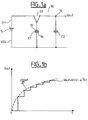
- FIG. 1a illustrates a representation of a basic circuit diagram of a charge pump circuit 10.
- This charge pump circuit 10 comprises a voltage supply 5, providing a voltage Vin, a unipolar switch with two contacts S1 and first and second capacitors C1, C2 .
- the switch S1 passes from its first position to its second position, the second position being indicated by dotted lines.
- the capacitors C1 and C2 are now connected in parallel between the output terminal 16 and the negative voltage terminal VSS and the two capacitors (C1, C2) are isolated from the voltage supply 5.
- the total charge which has summer stored by capacitors C1 and C2 at time t (n), that is to say Qt (n) is now shared between capacitors C1 and C2 and it follows that the voltage Vout increases from a value Vout (n) towards a value Vout (n + 1).
- FIG. 1b illustrates a graphic representation of the speed of variation of the programming voltage Vout as a function of time, that is to say dVout / dt. It should be noted that the initial height of variation of the jump in voltage Vout is much greater than the height of variation of the jump in voltage Vout towards the end of its increase.
- the VPP voltage is produced, from an existing HI-V voltage (outside or inside the integrated circuit), by a circuit comprising a capacitor supplied by a constant current source which is supplied by this voltage HI-V.
- a circuit comprising a capacitor supplied by a constant current source which is supplied by this voltage HI-V.
- Such a circuit suffers from the drawbacks of being analog and from the need to control the time when VPP reaches its nominal value, and to control the duration of a level value. This is also achieved by analog circuits which are difficult to adjust due to the dispersion of the characteristics.
- an object of the present invention is to generate a ramp voltage which is obtained from a given voltage.
- the given voltage can, but this is not necessary, have a value lower than the nominal ramp voltage.
- the means for generating the ramp voltage includes means for sampling the given voltage and means for regulating the ramp voltage to a desired value.
- the means for sampling the given voltage is connected, controlled and further directed so that the ramp voltage increases in a gradually controlled manner, the gradual increase in the ramp voltage being substantially linear.
- the subject of the invention is therefore a digital ramp generator characterized in that it comprises a controlled sampling circuit which receives an input voltage and produces a sampled voltage, an addition circuit for adding said sampled voltage to a generator output voltage (VPP) to provide a new voltage which is greater than said input voltage, and a transmission circuit, or voltage follower circuit, receiving said new voltage and said generator output voltage and providing a another generator output voltage greater than the previous generator output voltage.
- VPP generator output voltage
- FIG. 1a illustrates an already described representation of a diagram of a basic circuit of a charge pump circuit.
- FIG. 1b illustrates a graphical representation of the rate of variation of the output voltage Vout of FIG. 1a.
- Figure 2a illustrates a ramp generator digital according to the present invention.
- FIG. 2b illustrates the speed of variation of the programming voltage of FIG. 2a as a function of time.
- FIG. 2c illustrates the timing relationship of the control signals of the three switches as described in relation to FIGS. 2a and 2b.
- Figures 3a, 3b and 3c illustrate an example of a circuit diagram of the digital ramp generator of Figure 2a.
- Figure 4 shows the signals used to control the circuits of Figures 3a to 3c.
- Figure 5 shows a block diagram of a control signal generator which is used to produce the voltage levels of Figure 4.
- FIG. 2a is a representative illustration of a digital ramp generator according to the present invention.
- This digital ramp generator 20 comprises two unipolar switches with two contacts S20 and S22, a unipolar switch with a contact S24, three capacitors C20, C22, C24 and a voltage follower 22.
- a first contact of the switch S20 identified by the node 23 is connected to Vcc, its second contact is identified by the node 24 and its common node is identified by the node 25.
- the node 25 is connected to the node 23.
- the node 25 is connected to the node 24.
- a first contact of the switch S22 is identified by the node 26, its second contact is identified by the node 27 and its common node is identified by the node 28.
- the node 28 In a first position of the switch S22, the node 28 is connected to the node 26. In a second position, the node 28 is connected to the node 27.
- the node 23 is connected to a power input Vcc
- the node 26 is connected to a ground input, ie VSS.
- the capacitor C22 is connected between the node 24 and the reference voltage VSS.
- the node 24 provides a ramp voltage.
- the voltage follower 22 receives this ramp voltage on a first input and provides a VPP ramp output voltage on its output terminal 29.
- the output terminal 29 is connected to a second input of the voltage follower 22.
- the follower of voltage 22 could be an operational amplifier connected as a voltage follower. Schematically, the voltage follower 22 is supplied by a high input voltage HI-V.
- the switch 24 is connected in series between the nodes 27 and 29 and the capacitor C24 is connected between the node 27 and the voltage reference VSS.
- the capacitor C20 is connected between the nodes 25 and 28 of the switches S20 and S22, respectively.
- an unregulated programming supply voltage HI is regulated to its required value HI-V by means not shown.
- FIG. 2b illustrates the speed of variation of the programming voltage of FIG. 2a as a function of time.
- switches S20 and S22 are in their respective first position, as indicated by a solid line, and switch S24 is open: thus, the three capacitors C20, C22, C24 are all physically isolated from each other.
- the positive plate 25 of the capacitor C20 charges up to the voltage value Vcc, assuming that the voltage VSS is referenced with respect to ground via the switch S22.
- switches S20 and S22 switch, at the same time, or practically at the same time, from their first respective position to their second respective position, as indicated by dotted lines; switch S24 remains open.
- equation 2 remains true even during the following cycles. It will be noted that equation 2 does not contain a term VPP (t) on the right, unlike equation 1. The absence of term VPP (t) in the right member of equation 2 is at l he origin of the great improvement in the linearity of the slope of the voltage VPP, that is to say dVPP / dt.
- VPP [C20 / (C20 + C22)].
- A.Vcc.t where A is a constant which is proportional to the switching frequency of switches S20 and S22.
- the voltage VPP on the output terminal 29 of the voltage follower 22 follows or continues the voltage on its input terminal 24. Therefore, like the input terminal of the voltage follower voltage 22 is connected to node 24, the voltage VPP on the output terminal 29 of the voltage follower 22 is practically equal to the voltage given by equation 3.
- the switches S20 and S22 switch from their respective second position and return to their respective first position, the switch S24 remains open.
- the three capacitors, C20, C22, C24 are again all isolated from each other.
- the capacitor C20 again begins to charge towards the voltage value Vcc, it begins again to take a sample of the voltage Vcc.
- the switches S20 and S22 are in their first respective position, the positive plate 25 of the capacitor C20 is recharged at the voltage value Vcc.
- the level t2-t3 can be very short compared to the level t0-t1, t1-t2, or the next level t3-t4.
- the switches S20 and S22 always remain in their first respective position, the switch S24 closes and connects the output terminal 29 of the voltage follower 22 to the most positive plate 27 of the capacitor C24.
- the capacitor C24 is charged by the voltage VPP of the voltage follower present on the output terminal 29 of the voltage follower 22. That is to say that it is charged practically at the voltage value given by equation 3.
- the electrical charges come from the HI-V supply.
- the switch S24 opens and disconnects the output terminal 29 of the voltage follower 22 from the most positive plate 27 of the capacitor C24, which keeps practically his burden.
- the input sampling capacitor C20 always has a negative plate 28 referenced either to ground, or, by means of an output elevation capacitor C24, to the current value of the voltage of VPP output so that the input voltage Vcc is added to the current output voltage VPP.
- switches S20 and S22 switch from their respective second position and return to their first respective position and switch S24 remains open as described above for time t2.
- the switch S24 closes and connects the output terminal 29 of the voltage follower 22 to the positive plate 27 of the capacitor C24 as described above for time t3, and so on.
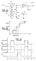
- Figure 2c illustrates the timing relationship of the respective control signals ⁇ 1, ⁇ 2 and ⁇ 3 of the respective switches S20, S22 and S24 as described in connection with Figures 2a and 2b.
- the duration of a cycle goes from time tl to time t5.
- FIG. 2c it is not compulsory to include the switch S24. It could in theory be replaced by a short circuit if the switches S20 and S22 were controlled so that the switch S20 is never in its first position when the switch S22 is in its second position (and vice versa). Although this leads to an unstable circuit in some cases, it could work.
- Figure 3a illustrates an example of a circuit diagram of the digital ramp generator of Figure 2a.
- This circuit diagram shows six N-type CMOS transistors MN1 to MN6, a diode D and the three capacitors C20, C22 and C24.
- transistor MN1 its source terminal represents node 23 and is preferably connected to a supply voltage VZ.
- the voltage VZ is produced by the circuit of FIG. 3b.
- the value of VZ is of the order of Vcc but in pulsed form.
- the drain terminal of MN1 represents node 25 and is connected to the positive plate of capacitor C20.
- transistor MN2 its drain terminal represents node 25 and its source terminal represents node 24, which is connected to the plate positive of capacitor C22.
- the transistors MN1 and MN2 are connected and controlled in such a way that they represent the switch S20 in FIG. 2a.
- the respective gate terminals of the transistors MN1 and MN2 are controlled by the respective control signals ⁇ 1 and N ⁇ 1.
- the signal N ⁇ 1 is the inverse signal of ⁇ 1.
- transistor MN3 its drain terminal represents the node 28 and is connected to the negative plate of the capacitor C20, its source terminal represents the node 26 and is connected to the negative voltage terminal VSS.
- transistor MN4 its source terminal represents node 28 and its drain terminal represents node 27, which is connected to the positive plate of capacitor C24.
- the transistors MN3 and MN4 are connected and controlled so that they represent the switch S22 in FIG. 2a.
- the respective gate terminals of the transistors MN3 and MN4 are controlled by the respective control signals ⁇ 2 and N ⁇ 2.
- the signal N ⁇ 2 is the inverse signal of ⁇ 2.
- the transistor MN5 is connected and controlled in such a way that it represents the voltage follower 22 of FIG. 2a.
- transistor MN5 its drain terminal is connected, via diode D, to node 25, that is to say the positive plate of capacitor C20.
- node 25 that is to say the positive plate of capacitor C20.
- Its gate terminal is connected to node 24, that is to say the positive plate of capacitor C22, and its source terminal represents node 29.
- Its drain terminal is connected to a HI-V node.
- the diode D is represented by a CMOS transistor of the N type connected in diode in the direct direction whose anode, which is connected to the node 25, is formed in connecting the gate and drain terminals together, the cathode of this diode, that is to say the source terminal, is connected to the drain terminal of the transistor MN5 and to the node HI-V. It is preferable to include this diode D insofar as it prevents any overvoltage from occurring at node 25, which can be produced by the elevation effect.
- the transistor MN6 is connected and controlled so that it represents the switch S24 in FIG. 2a. Referring to transistor MN6, its drain terminal is connected to the source terminal 29 of transistor MN5, its source terminal is connected to the positive plate 24 of capacitor C24 and its gate terminal is controlled by the control signal ⁇ 3 .
- control signals ⁇ 1, N ⁇ 1, ⁇ 2, N ⁇ 2 and ⁇ 3 are preferably obtained from circuits which are supplied from the high voltage HI-V, as described below.
- the transistors MN1 to MN6 are symmetrical CMOS transistors and that their respective drain and source terminals can be respectively interchanged. Furthermore, it is preferable that the transistors MN2 and MN5 are native N-type MOS transistors, that is to say transistors which have not been subject to gate threshold voltage adjustment (Vth ) and, consequently, have a low conduction threshold.
- Vth gate threshold voltage adjustment
- FIG. 3b represents a circuit preferably used to produce a voltage at a value VZ. Since identical electrical charges constitute the basic principle of a linear ramp signal, the sampling capacitor C20 should preferably be supplied with a constant voltage.
- the VZ power supply is produced by a Zener DZ diode, connected between a node HI-V voltage and a VSS voltage node, in series with a P type MP6 CMOS transistor. Furthermore, since such a circuit consumes current, it is preferable for it to be switched by a cyclic signal VE.
- the signal VE allows the conduction of the MP6-DZ circuit only when C20 must be charged: when the switches S20 and S22 switch to their first position.
- Conduction occurs for three microseconds every 16 microseconds.
- Conduction is obtained by means of a current mirror comprising the transistor MP6 in the branch of the diode DZ and a transistor MP5 in a branch further comprising a series of two MOS transistors of the N type MN12 and MN13.
- the transistor MN12 is used to condition the conduction of the diode DZ on the reception of signals VE on its gate.
- the gate of the transistor MP5 is connected to the gate of the transistor MP6 and to its own drain.
- the transistor MP5 acts as a current generator whose value is fixed by a constant voltage Vref appearing on the gate of the transistor MN13.
- the constant voltage Vref is itself produced by a conventional WILSON mirror circuit comprising CMOS transistors of the P type MP1 to MP4 and CMOS transistors of the N type MN10, MN11 and MN14.
- This WILSON mirror is itself switched by a signal VF which is applied to the gate of the copy transistor MP1 and MP2.
- VF is at VZ and the transistors MP1 and MP2 are blocked.
- VPP is required, VF is set to VSS.
- FIG. 3c represents a high voltage inverter circuit intended to generate the high voltage control signals ⁇ x and N ⁇ x.
- two circuits of this type are necessary to drive the switches S20 and S24 respectively.
- the high voltage inverter 400 shown comprises: a crossed stage 410; a cascode 420 stage; and a switching stage 430. It provides the complementary high voltage signals ⁇ x, N ⁇ x.
- the cross stage 410 is connected to the HI-V voltage and provides two complementary high-voltage output signals OUT and NOUT on its respective output terminals 440 and 450.
- the cross stage 410 comprises two crossed P type MOS transistors MP40 and MP41 whose sources are connected to the HI-V voltage.
- the gate of transistor MP40 is connected to drain 440 of transistor MP41 and the gate of transistor MP41 is connected to drain 450 of transistor MP40.
- L cascode stage 420 includes two MOS transistors of type P MP42 and MP43 whose source terminals are respectively connected to the drain terminals of transistors MP40 and MP41 and whose gate terminals are biased via terminal 480 by a voltage Vrefl reference.
- Vref1 is equal to HI-V minus around 5 volts.
- the drains of the MOS transistors MP40 and MP41 of stage 410 are thus polarized so as not to be at one voltage too low. This limits the switching current and thereby increases the efficiency since the circuit is supplied by the HI-V voltage source whose fan-out is low.
- Two respective input terminals of the switching stage 430 are connected to the respective output terminals 460 and 470 of the cascode stage 420.
- the switching stage 430 is controlled by means of a third input terminal 490, by an input control signal VC or VD (depending on the signals ⁇ 1 or ⁇ 2 to be produced) and is connected to the voltage source VSS.
- the voltage levels of the input control signals VC or VD are preferably obtained from the voltage source Vcc.
- the switching stage 430 comprises two N-type MOS transistors MN40 and MN41 and an inverter INV1, preferably a CMOS inverter.
- the drain terminals of the transistors MN40 and MN41 are respectively connected to the source terminals of the transistors MP42 and MP43.
- the control signals VC or VD are applied to the gate terminal of the transistor MN40 and to the input terminal of the inverter INV1.
- the gate terminal of the transistor MN41 is connected to the output terminal 495 of the inverter INV1.
- a high power pole of the inverter INV1 is connected to the voltage source VCC, while the low power pole of the inverter INV1 is connected to the voltage source VSS.
- the operation of the high-voltage inverter circuit 400 is symmetrical, only its operation in a high stable logic state, that is to say a voltage level of VCC, present on the gate terminal 490 of the transistor MN40 will be envisaged, since a person experienced in the technique can easily deduce the opposite case.
- the transistor MN40 is conductive while the transistor MN41 is not conductive.
- the transistor MN40 lowers the voltage on the drain terminal 470 of the transistor MP42 to a level approximately equal to VSS.
- the transistor MP42 (and in fact the transistor MP43) is switched by Vrefl via the terminal 480, it is conductive, it follows that the voltage of the node 450 is lowered to a level approximately equal to VPP-Vref1 + Vtp.
- the Vtp supplement is due to the fact that the boxes in which the P MP40 and MP43 transistors are manufactured are brought to HI-V.
- control signal ⁇ x is at a voltage level approximately equal to VPP
- control signal N ⁇ x is at a voltage level approximately equal to VSS.
- the signals ⁇ x and N ⁇ x are in phase opposition while the signals ⁇ x and VC or VD are in phase.
- control signal N ⁇ 2 can be the control signal ⁇ 1 and the control signal N ⁇ 1 can be the control signal ⁇ 2.
- these four control signals ⁇ 1, N ⁇ 1, ⁇ 2, N ⁇ 2 can be obtained from the same voltage level converter circuit; the control signal ⁇ 3 being obtained from another high voltage inverter.
- the control signals ⁇ 1, N ⁇ 1 and ⁇ 2, N ⁇ 2 can be obtained from different high voltage inverters.
- the transistor MN6 in FIG. 3 is controlled by the control signal ⁇ 2 (or N ⁇ 1) instead of ⁇ 3.
- FIG. 4 represents chronograms of the signals VC, VD, VE and VF presented above.
- VF is low when a VPP output is to be produced as a ramp.
- VE which triggers the conduction of DZ, is active at the end of an active pulse VD, which itself triggers the switches S20 and S22.
- VD active pulse
- VD active pulse
- FIG. 5 represents a block diagram of a control signal generator 500 which is used to generate the signals of FIG. 4.
- the generator 500 comprises an oscillator 510, a counter 520 and a decoder 530.
- the oscillator 510 drives the counter 520 and the decoder 530 receives from the counter 520 a plurality of input signals I1 to In and the decoder 530 delivers a plurality of control signals VC to VF which have the appropriate timing relationships.
- the decoder 530 and the counter 520 are known to persons skilled in the art.
- the operation of the digital ramp generator can be controlled by an ON / OFF signal which is received by the counter 520.
- the speed of variation of the programming voltage VPP that is to say dVPP / dt, will only depend on the ratio of the capacities C20 and C22, i.e. C20 / C22, which is an area ratio that can be controlled with precision.
- the digital ramp generator according to the invention is independent of all variations in process, temperature and supply voltage (VCC) and the programming voltage VPP at output 24 of the digital ramp generator is practically linear.
Landscapes
- Engineering & Computer Science (AREA)
- Power Engineering (AREA)
- Analogue/Digital Conversion (AREA)
- Dc-Dc Converters (AREA)
- Electronic Switches (AREA)
Applications Claiming Priority (2)
| Application Number | Priority Date | Filing Date | Title |
|---|---|---|---|
| FR9506498 | 1995-05-31 | ||
| FR9506498A FR2734941B1 (fr) | 1995-05-31 | 1995-05-31 | Generateur de rampe numerique. |
Publications (3)
| Publication Number | Publication Date |
|---|---|
| EP0745996A2 true EP0745996A2 (de) | 1996-12-04 |
| EP0745996A3 EP0745996A3 (de) | 1997-03-12 |
| EP0745996B1 EP0745996B1 (de) | 1999-04-07 |
Family
ID=9479569
Family Applications (1)
| Application Number | Title | Priority Date | Filing Date |
|---|---|---|---|
| EP96401155A Expired - Lifetime EP0745996B1 (de) | 1995-05-31 | 1996-05-29 | Digitaler Rampengenerator |
Country Status (4)
| Country | Link |
|---|---|
| US (1) | US5774390A (de) |
| EP (1) | EP0745996B1 (de) |
| DE (1) | DE69601976T2 (de) |
| FR (1) | FR2734941B1 (de) |
Cited By (2)
| Publication number | Priority date | Publication date | Assignee | Title |
|---|---|---|---|---|
| EP0862270A1 (de) * | 1997-02-28 | 1998-09-02 | STMicroelectronics S.r.l. | Adaptiver Treppenspannungserzeugerstromkreis |
| EP1017172A1 (de) * | 1998-12-29 | 2000-07-05 | STMicroelectronics S.r.l. | Mindestens eine spannungslineare Rampe mit geringer Steigung erzeugende integrierte Schaltung |
Families Citing this family (5)
| Publication number | Priority date | Publication date | Assignee | Title |
|---|---|---|---|---|
| FR2738386B1 (fr) * | 1995-09-05 | 1997-10-24 | Sgs Thomson Microelectronics | Procede et circuit de programmation et d'effacement d'une memoire |
| DE69922637D1 (de) | 1999-06-04 | 2005-01-20 | St Microelectronics Srl | CMOS Schalter zum Übertragen von hohen Spannungen, insbesondere für Zeilendekodierer in nichtflüchtigen Speichern mit geringem Verbrauch während des Schaltens |
| FI107478B (fi) | 1999-12-03 | 2001-08-15 | Nokia Networks Oy | Digitaalinen ramppigeneraattori, jossa on lähtötehon säädin |
| DE10227375A1 (de) * | 2002-06-20 | 2004-01-15 | Infineon Technologies Ag | Verfahren zur Erhöhung der Eingangsspannung einer integrierten Schaltung mittels einer zweistufigen Ladungspumpe sowie integrierte Schaltung |
| US7230561B2 (en) * | 2005-01-27 | 2007-06-12 | Micron Technology, Inc. | Programmable integrating ramp generator and method of operating the same |
Family Cites Families (1)
| Publication number | Priority date | Publication date | Assignee | Title |
|---|---|---|---|---|
| US5315547A (en) * | 1988-07-11 | 1994-05-24 | Hitachi, Ltd. | Nonvolatile semiconductor memory device with selective tow erasure |
-
1995
- 1995-05-31 FR FR9506498A patent/FR2734941B1/fr not_active Expired - Fee Related
-
1996
- 1996-05-29 DE DE69601976T patent/DE69601976T2/de not_active Expired - Fee Related
- 1996-05-29 EP EP96401155A patent/EP0745996B1/de not_active Expired - Lifetime
- 1996-05-30 US US08/652,710 patent/US5774390A/en not_active Expired - Lifetime
Cited By (4)
| Publication number | Priority date | Publication date | Assignee | Title |
|---|---|---|---|---|
| EP0862270A1 (de) * | 1997-02-28 | 1998-09-02 | STMicroelectronics S.r.l. | Adaptiver Treppenspannungserzeugerstromkreis |
| US5949666A (en) * | 1997-02-28 | 1999-09-07 | Sgs-Thomson Microelectronics S.R.L. | Staircase adaptive voltage generator circuit |
| EP1017172A1 (de) * | 1998-12-29 | 2000-07-05 | STMicroelectronics S.r.l. | Mindestens eine spannungslineare Rampe mit geringer Steigung erzeugende integrierte Schaltung |
| US6388505B1 (en) | 1998-12-29 | 2002-05-14 | Stmicroelectronics S.R.L. | Integrated circuit generating a voltage linear ramp having a low raise |
Also Published As
| Publication number | Publication date |
|---|---|
| FR2734941A1 (fr) | 1996-12-06 |
| EP0745996A3 (de) | 1997-03-12 |
| US5774390A (en) | 1998-06-30 |
| DE69601976T2 (de) | 1999-09-09 |
| EP0745996B1 (de) | 1999-04-07 |
| DE69601976D1 (de) | 1999-05-12 |
| FR2734941B1 (fr) | 1997-07-18 |
Similar Documents
| Publication | Publication Date | Title |
|---|---|---|
| FR2689340A1 (fr) | Circuit de pompage de charge pour un générateur de tension de substrat dans un dispositif de mémoire à semi-conducteur. | |
| EP2047475A2 (de) | Schaltung zur auslesung eines ladungszurückhaltungselements zur zeitmessung | |
| FR2690748A1 (fr) | Circuit de détection de seuil de tension à très faible consommation. | |
| EP2726905A2 (de) | Strahlungsdetektor mit einer schaltung zur einspeisung einer kalibrierten menge von gegenladungen | |
| EP0745996B1 (de) | Digitaler Rampengenerator | |
| EP0750244B1 (de) | Ladungspumpe-Generator-Schaltkreis für negative Spannung | |
| EP0323367B1 (de) | Einschalt-Rücksetzschaltung für eine integrierte Schaltung in MOS-Technik | |
| EP0902437B1 (de) | Hochspannungsgeneratorschaltung zum Programmieren oder Löschen eines Speichers | |
| EP3806162A1 (de) | Löschschaltung einer spad | |
| FR3068187A1 (fr) | Circuit a pompe de charges negative | |
| FR2886783A1 (fr) | Pompe a charge bi-directionnelle a haut rendement | |
| EP3032729A1 (de) | Gleichstrom-gleichstrom-wandler mit kaltstart | |
| FR2797119A1 (fr) | Dispositif de commande d'un commutateur haute tension de type translateur | |
| EP0379454B1 (de) | Von einer Vorrichtung mit zwei symmetrischen Ladungspumpen gesteuerte Leistungs-MOS-Transistorschaltung | |
| FR2490895A1 (fr) | Circuit d'entretien pour oscillateur a faible consommation de courant | |
| CA2328575C (fr) | Circuit de lecture de charges protege contre des surcharges provenant de charges de polarite non desiree | |
| EP1258975B1 (de) | Regelungsschaltung für Hochspannungsgenerator | |
| EP0076195B1 (de) | Anordnung zur Stromauslesung einer Ladungsquantität und Ladungsübertragungsfilter mit solch einer Anordnung | |
| FR2847717A1 (fr) | Circuit limiteur de tension, notamment pour pompe de charge | |
| FR2759507A1 (fr) | Pompe de charge dans une technologie a double caisson | |
| FR2758021A1 (fr) | Circuit elevateur de tension | |
| FR2529703A1 (fr) | Circuit dynamique generateur d'impulsions de source d'entree d'un dispositif a couplage de charge | |
| FR2677771A1 (fr) | Circuit de detection de niveau de polarisation inverse dans un dispositif de memoire a semiconducteurs. | |
| FR3103581A1 (fr) | Pompe de charge | |
| EP0690575B1 (de) | Vorrichtung zur Aktivierung einer Vorspannungsquelle |
Legal Events
| Date | Code | Title | Description |
|---|---|---|---|
| PUAI | Public reference made under article 153(3) epc to a published international application that has entered the european phase |
Free format text: ORIGINAL CODE: 0009012 |
|
| AK | Designated contracting states |
Kind code of ref document: A2 Designated state(s): DE FR GB IT |
|
| PUAL | Search report despatched |
Free format text: ORIGINAL CODE: 0009013 |
|
| AK | Designated contracting states |
Kind code of ref document: A3 Designated state(s): DE FR GB IT |
|
| 17P | Request for examination filed |
Effective date: 19970729 |
|
| 17Q | First examination report despatched |
Effective date: 19971013 |
|
| GRAG | Despatch of communication of intention to grant |
Free format text: ORIGINAL CODE: EPIDOS AGRA |
|
| GRAG | Despatch of communication of intention to grant |
Free format text: ORIGINAL CODE: EPIDOS AGRA |
|
| GRAH | Despatch of communication of intention to grant a patent |
Free format text: ORIGINAL CODE: EPIDOS IGRA |
|
| GRAH | Despatch of communication of intention to grant a patent |
Free format text: ORIGINAL CODE: EPIDOS IGRA |
|
| RAP3 | Party data changed (applicant data changed or rights of an application transferred) |
Owner name: STMICROELECTRONICS S.A. |
|
| GRAA | (expected) grant |
Free format text: ORIGINAL CODE: 0009210 |
|
| AK | Designated contracting states |
Kind code of ref document: B1 Designated state(s): DE FR GB IT |
|
| REF | Corresponds to: |
Ref document number: 69601976 Country of ref document: DE Date of ref document: 19990512 |
|
| GBT | Gb: translation of ep patent filed (gb section 77(6)(a)/1977) |
Effective date: 19990528 |
|
| PLBE | No opposition filed within time limit |
Free format text: ORIGINAL CODE: 0009261 |
|
| STAA | Information on the status of an ep patent application or granted ep patent |
Free format text: STATUS: NO OPPOSITION FILED WITHIN TIME LIMIT |
|
| 26N | No opposition filed | ||
| REG | Reference to a national code |
Ref country code: GB Ref legal event code: IF02 |
|
| PGFP | Annual fee paid to national office [announced via postgrant information from national office to epo] |
Ref country code: GB Payment date: 20040526 Year of fee payment: 9 |
|
| PGFP | Annual fee paid to national office [announced via postgrant information from national office to epo] |
Ref country code: DE Payment date: 20040610 Year of fee payment: 9 |
|
| PG25 | Lapsed in a contracting state [announced via postgrant information from national office to epo] |
Ref country code: IT Free format text: LAPSE BECAUSE OF NON-PAYMENT OF DUE FEES;WARNING: LAPSES OF ITALIAN PATENTS WITH EFFECTIVE DATE BEFORE 2007 MAY HAVE OCCURRED AT ANY TIME BEFORE 2007. THE CORRECT EFFECTIVE DATE MAY BE DIFFERENT FROM THE ONE RECORDED. Effective date: 20050529 Ref country code: GB Free format text: LAPSE BECAUSE OF NON-PAYMENT OF DUE FEES Effective date: 20050529 |
|
| PG25 | Lapsed in a contracting state [announced via postgrant information from national office to epo] |
Ref country code: DE Free format text: LAPSE BECAUSE OF NON-PAYMENT OF DUE FEES Effective date: 20051201 |
|
| GBPC | Gb: european patent ceased through non-payment of renewal fee |
Effective date: 20050529 |
|
| PGFP | Annual fee paid to national office [announced via postgrant information from national office to epo] |
Ref country code: FR Payment date: 20060825 Year of fee payment: 11 |
|
| REG | Reference to a national code |
Ref country code: FR Ref legal event code: ST Effective date: 20080131 |
|
| PG25 | Lapsed in a contracting state [announced via postgrant information from national office to epo] |
Ref country code: FR Free format text: LAPSE BECAUSE OF NON-PAYMENT OF DUE FEES Effective date: 20070531 |