EP0747505A2 - Appareillage et méthode avec régulation de température pour la déposition d'un matériau - Google Patents
Appareillage et méthode avec régulation de température pour la déposition d'un matériau Download PDFInfo
- Publication number
- EP0747505A2 EP0747505A2 EP96201480A EP96201480A EP0747505A2 EP 0747505 A2 EP0747505 A2 EP 0747505A2 EP 96201480 A EP96201480 A EP 96201480A EP 96201480 A EP96201480 A EP 96201480A EP 0747505 A2 EP0747505 A2 EP 0747505A2
- Authority
- EP
- European Patent Office
- Prior art keywords
- substrate
- cooling block
- gap
- depositing
- supporting
- Prior art date
- Legal status (The legal status is an assumption and is not a legal conclusion. Google has not performed a legal analysis and makes no representation as to the accuracy of the status listed.)
- Granted
Links
- 238000000151 deposition Methods 0.000 title claims abstract description 77
- 238000000034 method Methods 0.000 title claims abstract description 40
- 239000000126 substance Substances 0.000 title claims abstract description 21
- 239000000758 substrate Substances 0.000 claims abstract description 155
- 238000001816 cooling Methods 0.000 claims abstract description 83
- 230000008021 deposition Effects 0.000 claims abstract description 55
- 229910003460 diamond Inorganic materials 0.000 claims abstract description 26
- 239000010432 diamond Substances 0.000 claims abstract description 26
- 239000007789 gas Substances 0.000 claims description 26
- 239000001257 hydrogen Substances 0.000 claims description 18
- 229910052739 hydrogen Inorganic materials 0.000 claims description 18
- UFHFLCQGNIYNRP-UHFFFAOYSA-N Hydrogen Chemical compound [H][H] UFHFLCQGNIYNRP-UHFFFAOYSA-N 0.000 claims description 17
- VNWKTOKETHGBQD-UHFFFAOYSA-N methane Chemical compound C VNWKTOKETHGBQD-UHFFFAOYSA-N 0.000 description 8
- 230000004907 flux Effects 0.000 description 7
- 125000006850 spacer group Chemical group 0.000 description 7
- 150000002431 hydrogen Chemical class 0.000 description 5
- 239000000463 material Substances 0.000 description 5
- 238000002258 plasma jet deposition Methods 0.000 description 5
- 239000012530 fluid Substances 0.000 description 4
- OKTJSMMVPCPJKN-UHFFFAOYSA-N Carbon Chemical compound [C] OKTJSMMVPCPJKN-UHFFFAOYSA-N 0.000 description 3
- 230000008859 change Effects 0.000 description 3
- 239000002826 coolant Substances 0.000 description 3
- 238000010586 diagram Methods 0.000 description 3
- 239000000203 mixture Substances 0.000 description 3
- XKRFYHLGVUSROY-UHFFFAOYSA-N Argon Chemical compound [Ar] XKRFYHLGVUSROY-UHFFFAOYSA-N 0.000 description 2
- 239000003570 air Substances 0.000 description 2
- UBAZGMLMVVQSCD-UHFFFAOYSA-N carbon dioxide;molecular oxygen Chemical compound O=O.O=C=O UBAZGMLMVVQSCD-UHFFFAOYSA-N 0.000 description 2
- -1 for example Substances 0.000 description 2
- 229910002804 graphite Inorganic materials 0.000 description 2
- 239000010439 graphite Substances 0.000 description 2
- 239000001307 helium Substances 0.000 description 2
- 229910052734 helium Inorganic materials 0.000 description 2
- SWQJXJOGLNCZEY-UHFFFAOYSA-N helium atom Chemical compound [He] SWQJXJOGLNCZEY-UHFFFAOYSA-N 0.000 description 2
- 239000011810 insulating material Substances 0.000 description 2
- 238000005086 pumping Methods 0.000 description 2
- 239000004065 semiconductor Substances 0.000 description 2
- 239000007787 solid Substances 0.000 description 2
- XLYOFNOQVPJJNP-UHFFFAOYSA-N water Substances O XLYOFNOQVPJJNP-UHFFFAOYSA-N 0.000 description 2
- 239000004215 Carbon black (E152) Substances 0.000 description 1
- ZOKXTWBITQBERF-UHFFFAOYSA-N Molybdenum Chemical compound [Mo] ZOKXTWBITQBERF-UHFFFAOYSA-N 0.000 description 1
- 206010042618 Surgical procedure repeated Diseases 0.000 description 1
- 229910052786 argon Inorganic materials 0.000 description 1
- 229910052799 carbon Inorganic materials 0.000 description 1
- 239000000919 ceramic Substances 0.000 description 1
- 238000005229 chemical vapour deposition Methods 0.000 description 1
- 239000002131 composite material Substances 0.000 description 1
- 150000001875 compounds Chemical class 0.000 description 1
- 238000010276 construction Methods 0.000 description 1
- 239000012809 cooling fluid Substances 0.000 description 1
- 238000005137 deposition process Methods 0.000 description 1
- 229930195733 hydrocarbon Natural products 0.000 description 1
- 150000002430 hydrocarbons Chemical class 0.000 description 1
- 239000011261 inert gas Substances 0.000 description 1
- 150000002500 ions Chemical class 0.000 description 1
- 229910052750 molybdenum Inorganic materials 0.000 description 1
- 239000011733 molybdenum Substances 0.000 description 1
- 230000003287 optical effect Effects 0.000 description 1
- 238000013021 overheating Methods 0.000 description 1
- 238000005240 physical vapour deposition Methods 0.000 description 1
- 238000005268 plasma chemical vapour deposition Methods 0.000 description 1
- 230000005855 radiation Effects 0.000 description 1
- 229910052710 silicon Inorganic materials 0.000 description 1
- 239000010703 silicon Substances 0.000 description 1
- 150000003377 silicon compounds Chemical class 0.000 description 1
- 238000009987 spinning Methods 0.000 description 1
- 230000007704 transition Effects 0.000 description 1
- 210000000707 wrist Anatomy 0.000 description 1
Images


Classifications
-
- C—CHEMISTRY; METALLURGY
- C23—COATING METALLIC MATERIAL; COATING MATERIAL WITH METALLIC MATERIAL; CHEMICAL SURFACE TREATMENT; DIFFUSION TREATMENT OF METALLIC MATERIAL; COATING BY VACUUM EVAPORATION, BY SPUTTERING, BY ION IMPLANTATION OR BY CHEMICAL VAPOUR DEPOSITION, IN GENERAL; INHIBITING CORROSION OF METALLIC MATERIAL OR INCRUSTATION IN GENERAL
- C23C—COATING METALLIC MATERIAL; COATING MATERIAL WITH METALLIC MATERIAL; SURFACE TREATMENT OF METALLIC MATERIAL BY DIFFUSION INTO THE SURFACE, BY CHEMICAL CONVERSION OR SUBSTITUTION; COATING BY VACUUM EVAPORATION, BY SPUTTERING, BY ION IMPLANTATION OR BY CHEMICAL VAPOUR DEPOSITION, IN GENERAL
- C23C16/00—Chemical coating by decomposition of gaseous compounds, without leaving reaction products of surface material in the coating, i.e. chemical vapour deposition [CVD] processes
- C23C16/44—Chemical coating by decomposition of gaseous compounds, without leaving reaction products of surface material in the coating, i.e. chemical vapour deposition [CVD] processes characterised by the method of coating
- C23C16/46—Chemical coating by decomposition of gaseous compounds, without leaving reaction products of surface material in the coating, i.e. chemical vapour deposition [CVD] processes characterised by the method of coating characterised by the method used for heating the substrate
- C23C16/463—Cooling of the substrate
-
- C—CHEMISTRY; METALLURGY
- C23—COATING METALLIC MATERIAL; COATING MATERIAL WITH METALLIC MATERIAL; CHEMICAL SURFACE TREATMENT; DIFFUSION TREATMENT OF METALLIC MATERIAL; COATING BY VACUUM EVAPORATION, BY SPUTTERING, BY ION IMPLANTATION OR BY CHEMICAL VAPOUR DEPOSITION, IN GENERAL; INHIBITING CORROSION OF METALLIC MATERIAL OR INCRUSTATION IN GENERAL
- C23C—COATING METALLIC MATERIAL; COATING MATERIAL WITH METALLIC MATERIAL; SURFACE TREATMENT OF METALLIC MATERIAL BY DIFFUSION INTO THE SURFACE, BY CHEMICAL CONVERSION OR SUBSTITUTION; COATING BY VACUUM EVAPORATION, BY SPUTTERING, BY ION IMPLANTATION OR BY CHEMICAL VAPOUR DEPOSITION, IN GENERAL
- C23C16/00—Chemical coating by decomposition of gaseous compounds, without leaving reaction products of surface material in the coating, i.e. chemical vapour deposition [CVD] processes
- C23C16/44—Chemical coating by decomposition of gaseous compounds, without leaving reaction products of surface material in the coating, i.e. chemical vapour deposition [CVD] processes characterised by the method of coating
- C23C16/458—Chemical coating by decomposition of gaseous compounds, without leaving reaction products of surface material in the coating, i.e. chemical vapour deposition [CVD] processes characterised by the method of coating characterised by the method used for supporting substrates in the reaction chamber
- C23C16/4582—Rigid and flat substrates, e.g. plates or discs
- C23C16/4583—Rigid and flat substrates, e.g. plates or discs the substrate being supported substantially horizontally
- C23C16/4586—Elements in the interior of the support, e.g. electrodes, heating or cooling devices
-
- C—CHEMISTRY; METALLURGY
- C23—COATING METALLIC MATERIAL; COATING MATERIAL WITH METALLIC MATERIAL; CHEMICAL SURFACE TREATMENT; DIFFUSION TREATMENT OF METALLIC MATERIAL; COATING BY VACUUM EVAPORATION, BY SPUTTERING, BY ION IMPLANTATION OR BY CHEMICAL VAPOUR DEPOSITION, IN GENERAL; INHIBITING CORROSION OF METALLIC MATERIAL OR INCRUSTATION IN GENERAL
- C23C—COATING METALLIC MATERIAL; COATING MATERIAL WITH METALLIC MATERIAL; SURFACE TREATMENT OF METALLIC MATERIAL BY DIFFUSION INTO THE SURFACE, BY CHEMICAL CONVERSION OR SUBSTITUTION; COATING BY VACUUM EVAPORATION, BY SPUTTERING, BY ION IMPLANTATION OR BY CHEMICAL VAPOUR DEPOSITION, IN GENERAL
- C23C16/00—Chemical coating by decomposition of gaseous compounds, without leaving reaction products of surface material in the coating, i.e. chemical vapour deposition [CVD] processes
- C23C16/44—Chemical coating by decomposition of gaseous compounds, without leaving reaction products of surface material in the coating, i.e. chemical vapour deposition [CVD] processes characterised by the method of coating
- C23C16/46—Chemical coating by decomposition of gaseous compounds, without leaving reaction products of surface material in the coating, i.e. chemical vapour deposition [CVD] processes characterised by the method of coating characterised by the method used for heating the substrate
-
- C—CHEMISTRY; METALLURGY
- C23—COATING METALLIC MATERIAL; COATING MATERIAL WITH METALLIC MATERIAL; CHEMICAL SURFACE TREATMENT; DIFFUSION TREATMENT OF METALLIC MATERIAL; COATING BY VACUUM EVAPORATION, BY SPUTTERING, BY ION IMPLANTATION OR BY CHEMICAL VAPOUR DEPOSITION, IN GENERAL; INHIBITING CORROSION OF METALLIC MATERIAL OR INCRUSTATION IN GENERAL
- C23C—COATING METALLIC MATERIAL; COATING MATERIAL WITH METALLIC MATERIAL; SURFACE TREATMENT OF METALLIC MATERIAL BY DIFFUSION INTO THE SURFACE, BY CHEMICAL CONVERSION OR SUBSTITUTION; COATING BY VACUUM EVAPORATION, BY SPUTTERING, BY ION IMPLANTATION OR BY CHEMICAL VAPOUR DEPOSITION, IN GENERAL
- C23C16/00—Chemical coating by decomposition of gaseous compounds, without leaving reaction products of surface material in the coating, i.e. chemical vapour deposition [CVD] processes
- C23C16/44—Chemical coating by decomposition of gaseous compounds, without leaving reaction products of surface material in the coating, i.e. chemical vapour deposition [CVD] processes characterised by the method of coating
- C23C16/52—Controlling or regulating the coating process
Definitions
- This invention relates to temperature control during material deposition and, more particularly, to obtaining uniform and repeatable temperature conditions when depositing a substance on a substrate.
- the invention is especially applicable to deposition of diamond by plasma jet.
- a plasma of a hydrocarbon and hydrogen can be obtained using electrical arcing, and the resultant plasma directed toward a substrate, so that polycrystalline diamond film is deposited on the substrate.
- a spacer between the underside of the substrate and a cooling block (or cooled mandrel) that is used to cool the substrate which receives a high heat flux from the hot plasma beam.
- the spacer which may be, for example, a graphite disc, facilitates the temperature transition between the bottom of the substrate (which may be, for example, at a temperature in the range 500 to 1100 degrees C) and the top surface of the cooling block (which may be, for example, at a temperature in the range 10 to 500 degrees C).
- the substrate, spacer, and cooling block are held together by bolting or clamping, and the composite thermal conductivity through these components is quite sensitive to the relative surface contours of the components and to the pressure with which the surfaces are pressed together.
- Non-uniformity of contact and/or pressure can lead to substantial temperature differences at the deposition surface which, in turn, can degrade the uniformity and quality of the diamond film being deposited.
- contact and/or pressure changes when a new substrate is put in place the substrate temperature will be different during deposition. The resultant lack of repeatable deposition conditions can also tend to degrade the overall quality of the diamond film being produced.
- a technique for depositing a substance on a surface of a substrate including the following steps: providing a cooling block having a surface that is cooled by heat exchange; supporting the substrate from the cooling block so that the bottom surface of the substrate is spaced from the cooling block surface by a gap; providing a gas in the gap; and depositing said substance on the top surface of the substrate.
- reference to deposition on the top surface of the substrate includes deposition on the substrate itself, as well as deposition on any layers over the substrate.
- At least 30 percent of the gas in the gap is hydrogen, and the size of the gap is in the range .01 centimeters to .30 centimeters.
- at least 80 percent of the bottom surface of the substrate is spaced from and opposes the cooling block by the gap standoff.
- the technique hereof is particularly advantageous for deposition of diamond film by CVD plasma deposition in a deposition chamber containing at least 30 percent hydrogen.
- the deposition chamber environment will be mostly hydrogen gas.
- the majority of the heat flowing from the substrate passes by thermal conduction across the gas gap.
- uniform and repeatable temperature conditions at the substrate deposition surface are more easily attainable, since there is no longer reliance on providing uniform and repeatable surface contact and pressure between a substrate, a solid spacer, and a cooling block.
- the technique hereof also greatly facilitates operation with a mechanical (or robot) arm within the chamber without the need for breaking vacuum to secure a new substrate in place, since the substrate can be positioned without the requirement for precise clamping or bolting pressure. In some configurations, no bolting or clamping is even necessary.
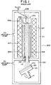
- Figure 1 is a schematic diagram, partially in block form, of a prior art apparatus in which the improvements of the invention can be utilized.
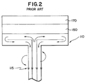
- Figure 2 is a simplified cross-sectional diagram which illustrates a prior art rotating mandrel assembly with heat exchange.
- Figure 3 is a cross-section of a model of a substrate and a cooling block separated by a gap.
- Figure 4 shows graphs of thermal conductivity as a function of temperature for hydrogen, helium, oxygen, carbon dioxide, and air.
- Figure 5 shows a cross-section of an arrangement of cooling block, substrate, and gas gap in accordance with an embodiment of the invention.
- Figures 6 and 7 show a further embodiment of the invention wherein a substrate holder is employed in spaced relation to the cooling block, and the cross-section of Figure 6 is a section taken through a plane represented by the arrows 6-6 in Figure 7.
- Figure 8 is top view of a further embodiment of the invention.
- Figure 9 is a cross-sectional partially broken away view which illustrates a further feature of the invention.
- Figure 10 is a cross-sectional view of a further embodiment of the invention.
- Figure 11 is a cross-sectional view of a further embodiment of the invention.
- Figures 12 and 13 show a further embodiment of the invention wherein a substrate holder is employed in space relation to a cooling block, and the cross-section of Figure 12 is a section taken through a plane represented by the arrows 12-12 in Figure 13.
- Figure 14 is a cross-sectional view of a further feature wherein injected gas is utilized.
- Figure 15 is a simplified diagram which shows the use of a robot arm in a deposition chamber.
- a deposition chamber 100 is the lower section of a plasma jet CVD deposition system 200, evacuated by one or more vacuum pumping systems (not shown).
- the system 200 is contained within a vacuum housing 211 and includes an arc-forming section 215 which comprises a cylindrical holder 294, a rod-like cathode 292, and an injector 295 mounted adjacent to the cathode so as to permit injected fluid to pass over the cathode.
- a cylindrical anode is provided at 291.
- the input fluid may be, for example, a mixture of hydrogen and methane. The methane could alternatively be fed in downstream.
- the anode 291 and cathode 292 are energized by a source of electrical power (not shown), for example a DC potential.
- Cylindrical magnets, designated by reference numeral 217 are utilized to help control the plasma generation.
- a nozzle, represented at 115, can be used to control beam size, within limitations.
- Optional cooling coils 234, in which a coolant can be circulated, can be located within the magnets.
- a mixture of hydrogen and methane is fed into the injector 295, and a plasma is obtained in front of the arc forming section and directed toward the deposition region at which a substrate is located.
- synthetic polycrystalline diamond can be formed from the described plasma, as the carbon in the methane is selectively deposited as diamond, and the graphite which forms is dissipated by combination with the hydrogen facilitating gas.
- suitable types of deposition equipment including, for example, other types of CVD deposition equipment, or physical vapor deposition equipment, can be used in conjunction with the features of the invention to be described.
- a mandrel 110 is rotatable on a shaft 111, and has a spacer 120 and a substrate 170 mounted thereon (by means not shown, bolting or clamping being typical).
- the mandrel 110 is a cooling block that can be cooled by any suitable means, for example by using a heat exchange fluid (e.g. water) that is circulated through the block or through another component in thermal contact with the block.
- a heat exchange fluid e.g. water
- the cooling block can be tilted with respect to the direction of the plasma jet, as disclosed in U.S. Patent No. 5,342,660, and a suitable motor (not shown) can be used for rotating the shaft, as is also disclosed in U.S. Patent No. 5,342,660.
- the rotational drive will conventionally be above the rotary union.
- the disclosed embodiments hereof can operate on a cooling block which is rotatable, as shown, or which is stationary.
- equation (2) can be used to compute the gap width that will handle the heat flux at the specified operating temperature differential.
- Figure 4 shows the thermal conductivity of hydrogen helium, oxygen, carbon dioxide, and air as a function of temperature. The curve values are approximately applicable over a range of operating pressures between .05 atmospheres and 10 atmospheres.
- the substrate back surface temperature is 700 degrees C and the cooling block surface temperature is 100 degrees C.
- the average temperature in the gap is about 400 degrees C and, at this temperature, Figure 4 shows that the thermal conductivity of hydrogen is about .0033 Watts/cm-°C.
- the CVD arc jet plasma deposition operates with a heat flux of 50 Watts/cm 2 , a substrate back surface temperature at 1000 degrees C, and a cooling block surface temperature of 125 degrees C.
- the cooling block 520 has a two-tiered annular shoulder 521 for supporting a disc-shaped substrate 510 above the cooling block top surface 525.
- the substrate can be any suitable material, for example, silicon.
- the structure 521 can be integral with the cooling block, or a separate unit as in some of the embodiments below.
- the cooling block 520 and its two-tiered annular support is similar to that of Figure 5.
- a disc-shaped substrate holder 610 is utilized.
- the substrate holder can be formed of any suitable material, for example, molybdenum.
- the substrate holder can hold substrates of any desired shape.
- the substrate holder has recesses that receive and hold cutting tool inserts 611, which are shown in a top view in Figure 7. Operation is similar to that previously described, with the gas gap providing the desired heat conduction path between the substrate holder and the cooling block at the desired operating temperatures to handle the heat flux into the substrates and substrate holder.
- a suitable substrate holder may be substituted for an illustrated substrate, or vice versa.
- Figure 8 shows, in a top view, that only three small sections of the two-tiered annular ridge 521 of the Figure 5 or Figure 6 embodiment need be utilized to hold the substrate.
- the three annular ridge sections, 521A, 521B, and 521C act as a frame that contacts the substrate or substrate holder over less area, to minimize thermal conduction from the substrate to the cooling block through the solid structure.
- the shoulder of each ridge can be provided with a pin 528 and pad 529, formed, for example, of a thermally insulating material such as a ceramic.
- the length of the pins 528 which are seated in receiving holes, can be used to adjust the gap standoff.
- the ridge for supporting the substrate or substrate holder is shown as part of the cooling block.
- the ridge or frame can be a separate piece or pieces.
- the ridge (or ridge sections) is on a ring 1021 that fits on the matching surface of cylindrical cooling block 1020.
- the ring or frame can be a two piece construction that holds and secures the substrate with screws 1140. The frame again fits on the cooling block 1020, as shown.
- FIGs 12 and 13 illustrate a further embodiment wherein the cooling block 1220 has three holes equidistant from the center thereof which receive respective pins 1201, 1202 and 1203.
- the distance of each pin from the center of the cylindrical cooling block corresponds to the radius of an annular groove 1214 in the bottom of a substrate holder 1210, so that when the substrate holder is placed over the cooling block, the pins engage the groove and define the offset of gap 1250.
- Different pin sizes can be used to obtain different gaps, and the pins can be formed of an insulating material to minimize thermal conduction through the pins.
- the annular rim shown at 1211 facilitates gripping of the substrate holder with a mechanical arm. If necessary or desirable, the substrate holder can be bolted or clamped in place by means not shown.
- the cooling block 1420 (or an attachment thereto, which is considered part of the cooling block for purposes hereof) can include inlet passages such as 1431 and 1432, and outlet passages 1435.
- a substrate or substrate holder 1410 is mounted as before.
- a gas can be injected into the inlet passages 1431 and 1432 and exhausted through the outlet passages 1435.
- a first gas such as hydrogen
- argon which has a much lower conductivity than hydrogen
- passages 1432 can be injected in a controlled manner into passages 1432 to control thermal conductivity of the gap 1410 as a function of radial position.
- a spatial variation of the gap thermal conductivity may also be established by varying the thickness of the gap as a function of radial position.
- Figure 15 generally represents a CVD plasma deposition chamber 1560 which may be of the type previously described, and which employs the gas gap feature hereof.
- the deposition chamber also includes a mechanical arm 1565 (sometimes called a robot arm) that can be controlled from outside the deposition chamber manually, automatically, or semi-automatically, to change substrates or substrate holders without the need for opening the chamber, so that appropriate pressure conditions need not be reestablished from scratch each time a new substrate is put in place.
- a mechanical arm 1565 sometimes called a robot arm
- the chamber can be initially provided with a supply of substrates or substrate holders (represented at 1510A) and, after deposition on a substrate (or substrates in a substrate holder) on the cooling block 1220, the robot arm 1565 can be operated to remove the substrate (or substrate holder) from the cooling block 1220, place it aside in the chamber (e.g. at 1510B), take another substrate (or substrate holder with substrates in place), and place it on the cooling block 1220. Deposition can then be implemented, and the substrate moving procedure repeated. If desired, each substrate in the supply can be pre-mounted in a ring structure as in Figure 11, so that the robot arm will handle the ring structure rather than the substrate itself.
- the robot arm 1565 can be of known type, which is articulated with an elbow 1566 and wrist 1567, and which engages and releases workpieces with a fork 1568.
- the robot arm, the supply of substrates, and/or other items can be in one or more auxiliary chambers, which can be considered as part of the main chamber for purposes hereof.
- a so-called "load lock" and/or any suitable valving arrangement can be used, as is known in the robotics art.
Landscapes
- Chemical & Material Sciences (AREA)
- General Chemical & Material Sciences (AREA)
- Chemical Kinetics & Catalysis (AREA)
- Engineering & Computer Science (AREA)
- Materials Engineering (AREA)
- Mechanical Engineering (AREA)
- Metallurgy (AREA)
- Organic Chemistry (AREA)
- Chemical Vapour Deposition (AREA)
- Crystals, And After-Treatments Of Crystals (AREA)
Applications Claiming Priority (2)
| Application Number | Priority Date | Filing Date | Title |
|---|---|---|---|
| US08/480,580 US5679404A (en) | 1995-06-07 | 1995-06-07 | Method for depositing a substance with temperature control |
| US480580 | 1995-06-07 |
Publications (3)
| Publication Number | Publication Date |
|---|---|
| EP0747505A2 true EP0747505A2 (fr) | 1996-12-11 |
| EP0747505A3 EP0747505A3 (fr) | 1998-03-11 |
| EP0747505B1 EP0747505B1 (fr) | 2003-09-17 |
Family
ID=23908514
Family Applications (1)
| Application Number | Title | Priority Date | Filing Date |
|---|---|---|---|
| EP96201480A Expired - Lifetime EP0747505B1 (fr) | 1995-06-07 | 1996-05-29 | Méthode avec régulation de température pour la déposition d'un matériau |
Country Status (5)
| Country | Link |
|---|---|
| US (2) | US5679404A (fr) |
| EP (1) | EP0747505B1 (fr) |
| JP (1) | JPH0925195A (fr) |
| CA (1) | CA2177645C (fr) |
| DE (1) | DE69629980T2 (fr) |
Cited By (2)
| Publication number | Priority date | Publication date | Assignee | Title |
|---|---|---|---|---|
| DE19718518A1 (de) * | 1997-05-02 | 1998-11-05 | Daimler Benz Ag | Verfahren und Vorrichtung zur Abscheidung von Diamant auf einem Substrat |
| WO2006120449A1 (fr) * | 2005-05-11 | 2006-11-16 | Surrey Nanosystems Limited | Procedes de production de nanostructures et appareil associe |
Families Citing this family (32)
| Publication number | Priority date | Publication date | Assignee | Title |
|---|---|---|---|---|
| US5679404A (en) * | 1995-06-07 | 1997-10-21 | Saint-Gobain/Norton Industrial Ceramics Corporation | Method for depositing a substance with temperature control |
| US6294025B1 (en) * | 1996-11-01 | 2001-09-25 | THEVA DüNNSCHICHTTECHNIK GMBH | Device for producing oxidic thin films |
| DE19718618C2 (de) * | 1997-05-02 | 1999-12-02 | Daimler Chrysler Ag | Komposit-Struktur mit einem mehrere mikroelektronische Bauteile und eine Diamantschicht aufweisenden Wachstums-Substrat sowie Verfahren zur Herstellung der Komposit-Struktur |
| US6328096B1 (en) * | 1997-12-31 | 2001-12-11 | Temptronic Corporation | Workpiece chuck |
| US6318957B1 (en) * | 1998-07-10 | 2001-11-20 | Asm America, Inc. | Method for handling of wafers with minimal contact |
| DE69935084T2 (de) * | 1998-07-31 | 2007-11-15 | Saint-Gobain Abrasives, Inc., Worcester | Drehende Abrichtrolle enthaltende abschleifende Einsätze |
| JP4260307B2 (ja) * | 1999-09-28 | 2009-04-30 | 芝浦メカトロニクス株式会社 | 気相成長装置 |
| CA2424029C (fr) | 2000-09-29 | 2008-01-29 | Cordis Corporation | Dispositifs medicaux enrobes |
| US20060222756A1 (en) * | 2000-09-29 | 2006-10-05 | Cordis Corporation | Medical devices, drug coatings and methods of maintaining the drug coatings thereon |
| DE10052724B4 (de) * | 2000-10-24 | 2012-08-02 | Pac Tech-Packaging Technologies Gmbh | Behandlungseinrichtung für Wafer |
| TW463326B (en) * | 2000-11-09 | 2001-11-11 | United Microelectronics Corp | Manufacturing method and structure of dynamic random access memory |
| TWI272689B (en) | 2001-02-16 | 2007-02-01 | Tokyo Electron Ltd | Method and apparatus for transferring heat from a substrate to a chuck |
| DE10149588B4 (de) * | 2001-10-08 | 2017-09-07 | Oerlikon Trading Ag, Trübbach | Verfahren zur Diamantbeschichtung von Substraten |
| JP3868324B2 (ja) * | 2002-04-15 | 2007-01-17 | 三菱電機株式会社 | シリコン窒化膜の成膜方法、成膜装置、及び半導体装置の製造方法 |
| JP3908112B2 (ja) * | 2002-07-29 | 2007-04-25 | Sumco Techxiv株式会社 | サセプタ、エピタキシャルウェーハ製造装置及びエピタキシャルウェーハ製造方法 |
| US7491234B2 (en) * | 2002-12-03 | 2009-02-17 | Boston Scientific Scimed, Inc. | Medical devices for delivery of therapeutic agents |
| US8555921B2 (en) | 2002-12-18 | 2013-10-15 | Vapor Technologies Inc. | Faucet component with coating |
| US7866343B2 (en) | 2002-12-18 | 2011-01-11 | Masco Corporation Of Indiana | Faucet |
| US7866342B2 (en) | 2002-12-18 | 2011-01-11 | Vapor Technologies, Inc. | Valve component for faucet |
| US6904935B2 (en) | 2002-12-18 | 2005-06-14 | Masco Corporation Of Indiana | Valve component with multiple surface layers |
| US8220489B2 (en) | 2002-12-18 | 2012-07-17 | Vapor Technologies Inc. | Faucet with wear-resistant valve component |
| US20040206304A1 (en) * | 2003-04-15 | 2004-10-21 | Menear John Edgar | Pressurized chuck for controlling backside wafer contamination |
| US9498563B2 (en) * | 2004-04-23 | 2016-11-22 | Boston Scientific Scimed, Inc. | Medical articles having therapeutic-agent-containing regions formed from coalesced polymer particles |
| US20070026205A1 (en) | 2005-08-01 | 2007-02-01 | Vapor Technologies Inc. | Article having patterned decorative coating |
| DE102006018514A1 (de) * | 2006-04-21 | 2007-10-25 | Aixtron Ag | Vorrichtung und Verfahren zur Steuerung der Oberflächentemperatur eines Substrates in einer Prozesskammer |
| GB201021913D0 (en) | 2010-12-23 | 2011-02-02 | Element Six Ltd | Microwave plasma reactors and substrates for synthetic diamond manufacture |
| CN102651331A (zh) * | 2011-06-14 | 2012-08-29 | 京东方科技集团股份有限公司 | 基板托盘及柔性电子器件制造方法 |
| US20140293291A1 (en) * | 2013-04-01 | 2014-10-02 | Kla-Tencor Corporation | Wafer Shape and Thickness Measurement System Utilizing Shearing Interferometers |
| DE102014104218A1 (de) * | 2014-03-26 | 2015-10-01 | Aixtron Se | CVD-Reaktor mit Vorlaufzonen-Temperaturregelung |
| CN215757604U (zh) * | 2021-01-25 | 2022-02-08 | 苏州晶湛半导体有限公司 | 石墨盘 |
| CN114334612B (zh) * | 2022-03-14 | 2022-06-28 | 广州粤芯半导体技术有限公司 | 半导体器件及其制造方法 |
| DE102024130537A1 (de) * | 2024-10-21 | 2026-04-23 | Condias Gmbh | Mit Diamant beschichtetes AIN-Substrat und Verfahren zum Herstellen |
Family Cites Families (53)
| Publication number | Priority date | Publication date | Assignee | Title |
|---|---|---|---|---|
| US3845739A (en) * | 1972-04-17 | 1974-11-05 | Xerox Corp | System for vapor deposition of thin films |
| CA1159012A (fr) * | 1980-05-02 | 1983-12-20 | Seitaro Matsuo | Dispositif de deposition de plasma |
| US4471003A (en) * | 1980-11-25 | 1984-09-11 | Cann Gordon L | Magnetoplasmadynamic apparatus and process for the separation and deposition of materials |
| US4487162A (en) * | 1980-11-25 | 1984-12-11 | Cann Gordon L | Magnetoplasmadynamic apparatus for the separation and deposition of materials |
| US4505947A (en) * | 1982-07-14 | 1985-03-19 | The Standard Oil Company (Ohio) | Method for the deposition of coatings upon substrates utilizing a high pressure, non-local thermal equilibrium arc plasma |
| JPS5921026A (ja) * | 1982-07-28 | 1984-02-02 | Hitachi Ltd | 半導体製造装置 |
| JPS5943861A (ja) * | 1982-09-03 | 1984-03-12 | Ulvac Corp | ル−バ−式化学的蒸着装置 |
| US4691662A (en) * | 1983-02-28 | 1987-09-08 | Michigan State University | Dual plasma microwave apparatus and method for treating a surface |
| US4507588A (en) * | 1983-02-28 | 1985-03-26 | Board Of Trustees Operating Michigan State University | Ion generating apparatus and method for the use thereof |
| US4585668A (en) * | 1983-02-28 | 1986-04-29 | Michigan State University | Method for treating a surface with a microwave or UHF plasma and improved apparatus |
| US4457259A (en) * | 1983-03-14 | 1984-07-03 | Rca Corporation | Apparatus for spraying a liquid on a spinning surface |
| US4527620A (en) * | 1984-05-02 | 1985-07-09 | Varian Associates, Inc. | Apparatus for controlling thermal transfer in a cyclic vacuum processing system |
| DE3422718A1 (de) * | 1984-06-19 | 1986-01-09 | Plasmainvent AG, Zug | Vakuum-plasma-beschichtungsanlage |
| US4630566A (en) * | 1984-08-16 | 1986-12-23 | Board Of Trustees Operating Michigan State University | Microwave or UHF plasma improved apparatus |
| US4728863A (en) * | 1985-12-04 | 1988-03-01 | Wertheimer Michael R | Apparatus and method for plasma treatment of substrates |
| JPH0772351B2 (ja) * | 1986-12-01 | 1995-08-02 | 株式会社日立製作所 | 金属薄膜選択成長方法 |
| JP2783796B2 (ja) * | 1987-05-22 | 1998-08-06 | キヤノン株式会社 | 堆積膜形成装置及びプラズマ処理装置 |
| JPH0193129A (ja) * | 1987-10-02 | 1989-04-12 | Mitsubishi Electric Corp | 化学気相成長装置 |
| JPH01242141A (ja) * | 1988-03-23 | 1989-09-27 | Hitachi Ltd | 高気圧マイクロ波プラズマ反応装置 |
| US4999320A (en) * | 1988-03-31 | 1991-03-12 | Texas Instruments Incorporated | Method for suppressing ionization avalanches in a helium wafer cooling assembly |
| JPH0757039B2 (ja) * | 1988-05-09 | 1995-06-14 | 株式会社ケンウッド | 音響用振動板及びその製造法 |
| US4949783A (en) * | 1988-05-18 | 1990-08-21 | Veeco Instruments, Inc. | Substrate transport and cooling apparatus and method for same |
| US5108779A (en) * | 1988-05-26 | 1992-04-28 | General Electric Company | Diamond crystal growth process |
| JPH01312008A (ja) * | 1988-06-11 | 1989-12-15 | Nkk Corp | 金属間化合物合金材の製造方法 |
| JPH0260103A (ja) * | 1988-08-26 | 1990-02-28 | Uchiya Thermostat Kk | 溶射技術を用いた抵抗体の製造方法 |
| JPH02167891A (ja) * | 1988-12-20 | 1990-06-28 | Citizen Watch Co Ltd | ダイヤモンド膜気相合成装置 |
| US5340401A (en) * | 1989-01-06 | 1994-08-23 | Celestech Inc. | Diamond deposition cell |
| US5104634A (en) * | 1989-04-20 | 1992-04-14 | Hercules Incorporated | Process for forming diamond coating using a silent discharge plasma jet process |
| US5094878A (en) * | 1989-06-21 | 1992-03-10 | Nippon Soken, Inc. | Process for forming diamond film |
| JPH0780718B2 (ja) * | 1989-08-04 | 1995-08-30 | トヨタ自動車株式会社 | ダイヤモンドの合成方法および合成装置 |
| JPH0687463B2 (ja) * | 1989-08-24 | 1994-11-02 | 株式会社東芝 | 半導体気相成長装置 |
| US5488774A (en) * | 1990-01-24 | 1996-02-06 | Janowski; Leonard J. | Cutting edges |
| US5132105A (en) * | 1990-02-02 | 1992-07-21 | Quantametrics, Inc. | Materials with diamond-like properties and method and means for manufacturing them |
| KR940011708B1 (ko) * | 1990-04-09 | 1994-12-23 | 니찌덴 아네루바 가부시끼가이샤 | 기판온도제어기구 |
| KR0165898B1 (ko) * | 1990-07-02 | 1999-02-01 | 미다 가쓰시게 | 진공처리방법 및 장치 |
| DE69127609T2 (de) * | 1990-07-18 | 1998-01-22 | Sumitomo Electric Industries | Vorrichtung und verfahren zur herstellung von diamanten |
| US5221403A (en) * | 1990-07-20 | 1993-06-22 | Tokyo Electron Limited | Support table for plate-like body and processing apparatus using the table |
| US5204145A (en) * | 1991-03-04 | 1993-04-20 | General Electric Company | Apparatus for producing diamonds by chemical vapor deposition and articles produced therefrom |
| ZA921208B (en) * | 1991-03-04 | 1993-02-24 | Gen Electric | Apparatus for producing diamonds by chemical vapor deposition and articles produced therefrom |
| US5342660A (en) * | 1991-05-10 | 1994-08-30 | Celestech, Inc. | Method for plasma jet deposition |
| US5204144A (en) * | 1991-05-10 | 1993-04-20 | Celestech, Inc. | Method for plasma deposition on apertured substrates |
| US5226383A (en) * | 1992-03-12 | 1993-07-13 | Bell Communications Research, Inc. | Gas foil rotating substrate holder |
| US5803977A (en) * | 1992-09-30 | 1998-09-08 | Applied Materials, Inc. | Apparatus for full wafer deposition |
| US5567267A (en) * | 1992-11-20 | 1996-10-22 | Tokyo Electron Limited | Method of controlling temperature of susceptor |
| JPH06244095A (ja) * | 1993-02-12 | 1994-09-02 | Dainippon Screen Mfg Co Ltd | 基板冷却装置 |
| DE4305750C2 (de) * | 1993-02-25 | 2002-03-21 | Unaxis Deutschland Holding | Vorrichtung zum Halten von flachen, kreisscheibenförmigen Substraten in der Vakuumkammer einer Beschichtungs- oder Ätzanlage |
| US5738165A (en) * | 1993-05-07 | 1998-04-14 | Nikon Corporation | Substrate holding apparatus |
| US5318801A (en) * | 1993-05-18 | 1994-06-07 | United States Of America As Represented By The Secretary Of The Navy | Substrate temperature control apparatus and technique for CVD reactors |
| TW277139B (fr) * | 1993-09-16 | 1996-06-01 | Hitachi Seisakusyo Kk | |
| US5595241A (en) * | 1994-10-07 | 1997-01-21 | Sony Corporation | Wafer heating chuck with dual zone backplane heating and segmented clamping member |
| JP4079992B2 (ja) * | 1994-10-17 | 2008-04-23 | バリアン・セミコンダクター・エクイップメント・アソシエイツ・インコーポレイテッド | 導電性被処理体を載置部材に締め付けるための装置及び静電クランピング方法 |
| US5551983A (en) * | 1994-11-01 | 1996-09-03 | Celestech, Inc. | Method and apparatus for depositing a substance with temperature control |
| US5679404A (en) * | 1995-06-07 | 1997-10-21 | Saint-Gobain/Norton Industrial Ceramics Corporation | Method for depositing a substance with temperature control |
-
1995
- 1995-06-07 US US08/480,580 patent/US5679404A/en not_active Expired - Fee Related
-
1996
- 1996-05-29 DE DE69629980T patent/DE69629980T2/de not_active Expired - Fee Related
- 1996-05-29 EP EP96201480A patent/EP0747505B1/fr not_active Expired - Lifetime
- 1996-05-29 CA CA002177645A patent/CA2177645C/fr not_active Expired - Fee Related
- 1996-06-07 JP JP8146131A patent/JPH0925195A/ja active Pending
-
1997
- 1997-05-27 US US08/863,763 patent/US6099652A/en not_active Expired - Fee Related
Cited By (6)
| Publication number | Priority date | Publication date | Assignee | Title |
|---|---|---|---|---|
| DE19718518A1 (de) * | 1997-05-02 | 1998-11-05 | Daimler Benz Ag | Verfahren und Vorrichtung zur Abscheidung von Diamant auf einem Substrat |
| DE19718518C2 (de) * | 1997-05-02 | 1999-11-04 | Daimler Chrysler Ag | Verfahren und Vorrichtung zur Abscheidung von Diamant auf einem Substrat und Verwendung |
| WO2006120449A1 (fr) * | 2005-05-11 | 2006-11-16 | Surrey Nanosystems Limited | Procedes de production de nanostructures et appareil associe |
| CN101213321B (zh) * | 2005-05-11 | 2010-12-08 | 萨里纳米系统有限公司 | 纳米结构体的制造方法和设备 |
| KR101368457B1 (ko) * | 2005-05-11 | 2014-03-12 | 서레이 나노시스템즈 리미티드 | 나노스트럭쳐 제조 방법 및 장치 |
| US9334167B2 (en) | 2005-05-11 | 2016-05-10 | Surrey Nanosystems Limited | Nanostructure production methods and apparatus |
Also Published As
| Publication number | Publication date |
|---|---|
| JPH0925195A (ja) | 1997-01-28 |
| CA2177645C (fr) | 2000-10-03 |
| EP0747505A3 (fr) | 1998-03-11 |
| DE69629980D1 (de) | 2003-10-23 |
| US6099652A (en) | 2000-08-08 |
| CA2177645A1 (fr) | 1996-12-08 |
| DE69629980T2 (de) | 2004-07-29 |
| US5679404A (en) | 1997-10-21 |
| EP0747505B1 (fr) | 2003-09-17 |
Similar Documents
| Publication | Publication Date | Title |
|---|---|---|
| US5679404A (en) | Method for depositing a substance with temperature control | |
| US5551983A (en) | Method and apparatus for depositing a substance with temperature control | |
| US5342660A (en) | Method for plasma jet deposition | |
| US5383971A (en) | Differential pressure CVD chuck | |
| US5935338A (en) | Chemical vapor deposition chamber | |
| EP0467390B1 (fr) | Plaque-support pour objet en forme de plaquette et dispositif de traitement utilisant cette plaque-support | |
| US5534072A (en) | Integrated module multi-chamber CVD processing system and its method for processing subtrates | |
| CA2138292C (fr) | Module de traitement a suscepteur tournant a galette de semiconducteur pour le depot de tungstene en phase vapeur | |
| US5753092A (en) | Cylindrical carriage sputtering system | |
| EP0646285B1 (fr) | Procede et appareil de traitement de tranches de semi-conducteurs a regulation du flux thermique et gazeux | |
| US6197121B1 (en) | Chemical vapor deposition apparatus | |
| US10051693B2 (en) | Apparatus and method for heating semiconductor wafers via microwaves | |
| KR20100016083A (ko) | 반도체 재료 프로세싱 장치용 저-입자 성능을 갖는 샤워헤드 전극 및 샤워헤드 전극 어셈블리 | |
| US20100151680A1 (en) | Substrate carrier with enhanced temperature uniformity | |
| JP2001512789A (ja) | ミニ・バッチ式プロセス・チャンバ | |
| US4651674A (en) | Apparatus for vapor deposition | |
| JP4471848B2 (ja) | 基板保持装置 | |
| EP0583374B1 (fr) | Procede et appareil de deposition par jet de plasma | |
| JPH0857753A (ja) | ダイヤモンドの加工方法および加工装置 | |
| JP3865841B2 (ja) | 電子ビーム蒸着装置 | |
| JP3081669B2 (ja) | 処理装置 | |
| WO2025155610A1 (fr) | Régulateur thermique pour le chauffage de substrats dans un outil de traitement | |
| CA2204164A1 (fr) | Procede et appareil permettant de deposer une substance dans des conditions de temperature regulee | |
| WO1996013623A1 (fr) | Procede et appareil permettant de deposer une substance dans des conditions de temperature regulee | |
| JPH03228320A (ja) | 薄膜形成装置 |
Legal Events
| Date | Code | Title | Description |
|---|---|---|---|
| PUAI | Public reference made under article 153(3) epc to a published international application that has entered the european phase |
Free format text: ORIGINAL CODE: 0009012 |
|
| AK | Designated contracting states |
Kind code of ref document: A2 Designated state(s): DE FR GB |
|
| PUAL | Search report despatched |
Free format text: ORIGINAL CODE: 0009013 |
|
| AK | Designated contracting states |
Kind code of ref document: A3 Designated state(s): DE FR GB |
|
| 17P | Request for examination filed |
Effective date: 19980911 |
|
| 17Q | First examination report despatched |
Effective date: 19981012 |
|
| RAP1 | Party data changed (applicant data changed or rights of an application transferred) |
Owner name: SAINT-GOBAIN INDUSTRIAL CERAMICS, INC. |
|
| GRAH | Despatch of communication of intention to grant a patent |
Free format text: ORIGINAL CODE: EPIDOS IGRA |
|
| RTI1 | Title (correction) |
Free format text: METHOD FOR DEPOSITING A SUBSTANCE WITH TEMPERATURE CONTROL |
|
| GRAS | Grant fee paid |
Free format text: ORIGINAL CODE: EPIDOSNIGR3 |
|
| GRAA | (expected) grant |
Free format text: ORIGINAL CODE: 0009210 |
|
| AK | Designated contracting states |
Kind code of ref document: B1 Designated state(s): DE FR GB |
|
| REG | Reference to a national code |
Ref country code: GB Ref legal event code: FG4D |
|
| REF | Corresponds to: |
Ref document number: 69629980 Country of ref document: DE Date of ref document: 20031023 Kind code of ref document: P |
|
| PGFP | Annual fee paid to national office [announced via postgrant information from national office to epo] |
Ref country code: FR Payment date: 20040519 Year of fee payment: 9 |
|
| PGFP | Annual fee paid to national office [announced via postgrant information from national office to epo] |
Ref country code: GB Payment date: 20040526 Year of fee payment: 9 |
|
| PGFP | Annual fee paid to national office [announced via postgrant information from national office to epo] |
Ref country code: DE Payment date: 20040630 Year of fee payment: 9 |
|
| ET | Fr: translation filed | ||
| PLBE | No opposition filed within time limit |
Free format text: ORIGINAL CODE: 0009261 |
|
| STAA | Information on the status of an ep patent application or granted ep patent |
Free format text: STATUS: NO OPPOSITION FILED WITHIN TIME LIMIT |
|
| 26N | No opposition filed |
Effective date: 20040618 |
|
| PG25 | Lapsed in a contracting state [announced via postgrant information from national office to epo] |
Ref country code: GB Free format text: LAPSE BECAUSE OF NON-PAYMENT OF DUE FEES Effective date: 20050529 |
|
| PG25 | Lapsed in a contracting state [announced via postgrant information from national office to epo] |
Ref country code: DE Free format text: LAPSE BECAUSE OF NON-PAYMENT OF DUE FEES Effective date: 20051201 |
|
| GBPC | Gb: european patent ceased through non-payment of renewal fee |
Effective date: 20050529 |
|
| PG25 | Lapsed in a contracting state [announced via postgrant information from national office to epo] |
Ref country code: FR Free format text: LAPSE BECAUSE OF NON-PAYMENT OF DUE FEES Effective date: 20060131 |
|
| REG | Reference to a national code |
Ref country code: FR Ref legal event code: ST Effective date: 20060131 |