EP0747860B1 - Méthode et système d'allocation de mémoire à des données de topographie de texture - Google Patents
Méthode et système d'allocation de mémoire à des données de topographie de texture Download PDFInfo
- Publication number
- EP0747860B1 EP0747860B1 EP96107383A EP96107383A EP0747860B1 EP 0747860 B1 EP0747860 B1 EP 0747860B1 EP 96107383 A EP96107383 A EP 96107383A EP 96107383 A EP96107383 A EP 96107383A EP 0747860 B1 EP0747860 B1 EP 0747860B1
- Authority
- EP
- European Patent Office
- Prior art keywords
- texture
- map
- cache
- data
- texel
- Prior art date
- Legal status (The legal status is an assumption and is not a legal conclusion. Google has not performed a legal analysis and makes no representation as to the accuracy of the status listed.)
- Expired - Lifetime
Links
Images


Classifications
-
- G—PHYSICS
- G06—COMPUTING OR CALCULATING; COUNTING
- G06F—ELECTRIC DIGITAL DATA PROCESSING
- G06F12/00—Accessing, addressing or allocating within memory systems or architectures
- G06F12/02—Addressing or allocation; Relocation
- G06F12/08—Addressing or allocation; Relocation in hierarchically structured memory systems, e.g. virtual memory systems
- G06F12/0802—Addressing of a memory level in which the access to the desired data or data block requires associative addressing means, e.g. caches
- G06F12/0844—Multiple simultaneous or quasi-simultaneous cache accessing
- G06F12/0846—Cache with multiple tag or data arrays being simultaneously accessible
-
- G—PHYSICS
- G06—COMPUTING OR CALCULATING; COUNTING
- G06F—ELECTRIC DIGITAL DATA PROCESSING
- G06F12/00—Accessing, addressing or allocating within memory systems or architectures
- G06F12/02—Addressing or allocation; Relocation
- G06F12/06—Addressing a physical block of locations, e.g. base addressing, module addressing, memory dedication
- G06F12/0607—Interleaved addressing
-
- G—PHYSICS
- G06—COMPUTING OR CALCULATING; COUNTING
- G06F—ELECTRIC DIGITAL DATA PROCESSING
- G06F12/00—Accessing, addressing or allocating within memory systems or architectures
- G06F12/02—Addressing or allocation; Relocation
- G06F12/08—Addressing or allocation; Relocation in hierarchically structured memory systems, e.g. virtual memory systems
- G06F12/0802—Addressing of a memory level in which the access to the desired data or data block requires associative addressing means, e.g. caches
- G06F12/0875—Addressing of a memory level in which the access to the desired data or data block requires associative addressing means, e.g. caches with dedicated cache, e.g. instruction or stack
-
- G—PHYSICS
- G06—COMPUTING OR CALCULATING; COUNTING
- G06T—IMAGE DATA PROCESSING OR GENERATION, IN GENERAL
- G06T15/00—Three-dimensional [3D] image rendering
- G06T15/04—Texture mapping
Definitions
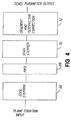
- the parameter interpolator circuit 64 shown in more detail in Fig. 4, includes an edge stepper 66, a FIFO ("first-in, first-out") buffer 68, a span stepper 70 and a gradient and perspective correction circuit 72, all connected in series.
- the edge stepper starts at the x,y pixel coordinate of one of the triangle vertices, and utilizing the triangle plane equation, steps the edges of the triangle to determine the pixel coordinates that define the triangle edges. For each pixel coordinate, texture map S and T coordinates are determined, based on the S,T values of the triangle vertices, to identify which texels in the texture map correspond to each display screen pixel coordinate.
- Each S and T coordinate for a display screen pixel may have an integer portion and a fractional portion if the pixel does not map directly (in one-to-one correspondence) to a single texel in one of the series of MIP maps for the texture.
- each display screen pixel when mapped to the texture map, may lie between multiple texels in one of the series of MIP maps for the texture, and furthermore, may lie between adjacent (in size) MIP maps in the series.
- the capability of allowing a pixel to map to a location in a texture map that is beyond its boundary provides flexibility in the manner in which textures can be mapped to object primitives. For example, it may be desirable to map a texture to an object in a repeating fashion, such that the texture is mapped to multiple portions of the object. For example, if a texture is defined having S,T coordinates ranging from [0, 0] inclusive through (10, 10) non-inclusive, a user could specify certain portions of the object to map to S,T coordinates [10, 10] inclusive through (20, 20) non-inclusive.
- the texture data (i.e., the MIP maps) is divided into texel blocks of data that each includes 256x256 texels.
- the cache memory can store as many as sixty-four blocks of data at one time. Each block has an associated block tag that uniquely identifies the block.
- the cache includes a cache directory 78 that stores the block tags that correspond to the blocks of data currently stored in the cache. As described in greater detail below, each block tag includes a texture identifier (texture ID) that identifies the particular texture that the block of data represents, a map number that identifies the particular MIP map within the texture's series of maps that the block of data represents, and high-order S and T coordinates that identify the location of the block of data within the particular map.
- the physical location of the block tag within the cache directory represents the location of the corresponding block of data within the cache memory.
- the tiler/boundary checker 72 During rendering, the tiler/boundary checker 72 generates a read cache tag for the block of texture data that maps to the pixel to be rendered.
- the manner in which the tags are generated is explained in more detail below.
- the tags are 23-bit fields that include eight bits representing the texture ID of the texture data, a bit used in determining the map number of the texture data, and the seven high-order S and T coordinates of the texture data.
- the cache directory 78 compares the read cache tag provided from the tiler/boundary with the block tags stored in the directory to determine whether the block of texture data to be used in rendering is in the cache memory.
- the cache directory 78 When the read cache tag does not match any of the block tags stored in the cache directory 78, a miss occurs and the cache directory 78 generates an interrupt control signal over line 94 (Fig. 2) to the distributor chip 30 on the front end board, which generates an interrupt over line 95 to the host computer 15.
- the processor 19 of the host computer executes a service routine, discussed in more detail below, which reads the missed block tag from the cache directory and downloads the corresponding block of texture data into the cache memory in a manner that bypasses the 3-D primitive pipeline in the front end board 10 and the texture mapping chip 46.
- the texture data downloaded from the main memory is provided over bus 24, through the texel port 92 (Fig. 3) to the texel cache access circuit 82, which writes the data to the SDRAMs that form the cache memory.
- the texture mapping chip waits for the new texture data to be downloaded before proceeding with processing the primitive on which the miss occurred.
- the stages of the pipeline that follow the cache read continue to process those primitives received prior to the miss primitive.
- the stages of the pipeline that precede the cache read also continue to process primitives unless and until the pipeline fills up behind the cache read operation while awaiting the downloading of the new texture data.
- the frame buffer board is provided with a deeper primitive pipeline than the texture mapping board, so that the texture mapping pipeline should not be delayed by waiting for the frame buffer pipeline to become available.
- the capability is provided to turn off texture mapping. This is accomplished by software operating on the processor 19 of the host computer to set a register in both the texture mapping board 12 and the frame buffer board 14. When set to turn off texture mapping, these registers respectively inhibit the texture mapping chip 46 from providing texture data to the frame buffer board 14, and instruct the frame buffer board to proceed with rendering primitives without waiting for texture data from the texture mapping board.
- texels from one MIP map may be accessed from the cache memory to determine the resultant texture data for the pixel.
- the texels read from the cache are provided over bus 86 (Fig 3) to the texel interpolator 76, which interpolates the multiple texels to compute resultant texel data for each pixel.
- the interpolation can vary depending upon a mode established for the system.
- the resultant texel data When a point sampling interpolation mode is established, the resultant texel data equals the single texel that is closest to the location defined by the pixel's S,T coordinates in the texture map.
- the resultant texel data is respectively a weighted average of the four or eight closest texels in the one or two closest maps. The weight given to each of the multiple texels is determined based upon the value of the gradient and the factional components of the S and T coordinates provided to the texel interpolator 76 from the tiler/boundary checker.
- the resultant texel data for the display screen pixels is sequentially provided over bus 88 to a frame buffer interface FIFO buffer 90.
- the frame buffer interface FIFO buffer 90 can store up to sixty four resultant texels.
- Each resultant texel is a 32-bit word including eight bits to represent each of R,G,B and ⁇ .
- the ⁇ byte indicates to the frame buffer board 14 (Fig. 2) the manner in which the R,G,B values of the resultant texture data should be combined with the R,G,B values of the object data generated by the frame buffer board in computing final display screen R,G,B values for any pixel that maps to the texel.
- the frame buffer interface FIFO buffer outputs T0-T4 are provided to the frame buffer board 14 (Fig. 2) over bus 28.
- the frame buffer board combines the R,G,B values of the resultant texel data with the object R,G,B values in the manner specified by ⁇ to generate final R,G,B values for each display screen pixel.
- Fig. 5 is a block diagram of a cache memory implementation according to one illustrative embodiment of the present invention, coupled to portions of the texture mapping chip including the texel port 92, texture interpolator 76, cache directory 78 and the texel cache access circuit 82.
- the cache memory 48 includes four interleaves 204A, 204B, 204C and 204D.
- Each interleave includes two SDRAM chips (not shown) that can be accessed simultaneously, with each providing eights bits of data during a read cycle. Therefore, each interleave provides sixteen bits of texel data during a single read cycle.
- the cache can be implemented in eight separate interleaves, with eight separate controllers so that when trilinear interpolation is employed, the eight texels can be accessed simultaneously from the cache in a single read operation.
- Each SDRAM chip in the cache memory is divided internally into two equally-sized banks that can simultaneously maintain separate active pages (i.e., groups of memory locations having a common row address).
- active pages i.e., groups of memory locations having a common row address
- the two SDRAMs in each interleave can be simultaneously accessed and together provide sixteen bits of data, with one of the SDRAMs providing data bits [15:08] and the other providing data bits [07:00].
- two consecutive read cycles of a single burst yield a full 32-bit texel of data from each interleave, with a separate 8-bit word representing each of the R, G, B and ⁇ values for the texel.
- the RAS, CAS, and WE lines are used to address and write data to the SDRAM chip in a conventional manner.
- the clock enable signal CKE signal is deasserted, the internal clock is suspended.
- the SDRAMs respond to this signal by holding data intact, rendering both banks idle.
- the data input/output mask DQM signal functions as an output enable during a read cycle, and an input data mask during a write cycle.
- the data from the separate banks can be accessed in consecutive read cycles without penalty. While the method of the present invention of data storage allocation for improving SDRAM performance has been shown and described with respect to the storage of texture mapping data, it should be understood that the method of the present invention is not so limited. Particularly, the method is applicable to allocate any type of data in which multiple consecutive read cycles access data from different memory locations.
- Fig. 8 is a more detailed block diagram of a portion of the texture mapping chip that includes the boundary checker 72, the cache directory 78, the cache access circuit 82, the cache memory 48 and the texel interpolator 76.
- the texel cache access unit 82 includes four cache access command FIFOs 206A, 206B, 206C and 206D.
- the cache access command FIFOs 206A-D store cache access commands respectively received from the boundary checker over 16-bit buses 84A, 84B, 84C and 84D.
- the cache access command FIFOs 206A-D respectively correspond to the controllers 200A-D shown in Fig. 6.
- each of the four interleaves of the cache memory can be accessed simultaneously through separate cache access paths.
- texel access control words are provided over buses 208A, 208B, 208C and 208D to the cache memory 48.
- Four texels are accessed simultaneously from the four interleaves during two back-to-back 16-bit read cycles.
- the four texels are respectively provided over buses 210A, 210B, 210C and 210D to one of the texel data A FIFOs (214A0 or 214A1), one of the texel data B FIFOs (214B0 or 214B), one of the texel data C FIFOs (214C0 or 214C1) and one of the texel data D FIFOs (214D0 or 214D1).
- the pair of texel data FIFOs i.e., zero and one
- corresponding to each interleave A-D are loaded in alternating fashion.
- a first texel read from interleave A is stored in texel data FIFO 214A0
- a second texel read from interleave A is stored in FIFO 214A1
- a third texel from interleave A is stored in FIFO 214A0, etc.
- This alternating scheme is employed for reasons that are discussed below.
- Each of the texel data FIFOs is thirty-two bits wide, and eight stages deep.
- the eight FIFOs 214 store eight pipelined stages, each stage including the eight texels used to determine resultant texel data during trilinear interpolation.
- Buses 210A, 210B, 210C and 210D are sixteen bits wide.
- Each SDRAM pair in each interleave provides sixteen bits of data during each read cycle. During each burst, the first sixteen bits are provided from each SDRAM pair into a first 16-bit register (not shown) and the next sixteen bits are provided from each SDRAM pair into a second 16-bit register (also not shown).
- the data from both registers is provided onto the corresponding 32-bit bus 212A, 212B, 212C or 212D.
- the texel interpolator 76 accesses the FIFOs to read the next stage of eight texels, and interpolates those texels in the manner described above.
- the resultant texel data is then provided over bus 28 to the frame buffer board 14 (Fig. 2) where it is used in the rendering the display screen pixel in the manner discussed above.
- the resultant texel data for any pixel is interpolated from four texels in one MIP map and four texels in an adjacent MIP map.
- Adjacent display screen pixels are generally rendered in succession. Often, adjacent display screen pixels will map to adjacent locations in a texture MIP map.
- it is common that some common texel data may be used in interpolating resultant texel data for consecutively rendered primitives.
- the cache when common texel data is accessed multiple times within a number of closely spaced read cycles, the cache is only accessed for the first read, saving cache read cycles for each successive read. The most recently read texels are stored within the texel data FIFOs. Thus, subsequent accesses to those texels are made from the FIFOs rather than the cache. This reduces the number of cache accesses required, thereby increasing system bandwidth.
- a cache access command is not provided to the corresponding cache access FIFO 206A, B, C or D. Instead, a command is sent to the texel interpolator to indicate that the texel data is stored in the most recently written location of the corresponding texel data FIFO 214A, B, C or D.
- a texel cache access command is provided to the corresponding texel cache access command FIFO to read that texel data from the cache memory 48.
- interleaves A-D for any pixel currently in the pipeline position for which a cache access must be considered.
- common texel data for consecutive pixels may exist for interleave A but not for interleaves B-D.
- texel data will be read from interleaves B-D for the second of the consecutive pixels in the pipeline position for accessing texel data from the cache, but the texel data from interleave A for that second pixel will be read from the same location of one of the texel data FIFOs 214A0 or 214A1.
- the present scheme provides bandwidth savings when texels are re-read from the texel data FIFOs for multiple pixels without accessing the cache..
- the texel interpolator 76 includes a texel interpolator command FIFO 216 that receives 53-bit commands from the boundary checker 72 over 53-bit bus 218.
- the texel interpolator command FIFO can store up to sixteen commands that indicate to the interpolator which texel data FIFO locations contain the texel data to be used in interpolating the resultant texel data during each cycle.
- the interpolator commands also indicate the mode of interpolation (i.e., point sampling, bilinear or trilinear), and include the gradient and fractional values of the S and T coordinates, which specify the manner in which each texel should be weighted in the interpolation.
- the commands include data indicating from which texel data FIFOs 214A0, A1, B0, B1, C0, C1, D0, or D1 each of the four (bilinear) or eight (trilinear) texels are to be read, and whether the texel data is new or old.
- Texel data is new when it is different from the texel data stored in the most recently written to location of either texel data FIFO of that path. When new, a cache read is required.
- Texel data is old when it is the same as that stored in the most recently written location of either texel data FIFO. When old, a cache read is not required.
- the FIFO read pointer When the texel data is new, the FIFO read pointer must be moved to a next location within the FIFO, whereas when the texel data is old, the same data is read from the same FIFO location and the read pointer need not be moved.
- Fig. 9 shows multiple texels of an upper MIP map and multiple texels of a lower (smaller in size) MIP map.
- the texels are labeled An, Bn, Cn and Dn (wherein n represents an integer) in accordance with the labeling scheme previously described with respect to Fig. 7.
- Seven pixels to be rendered are labeled P0, P1, ... P6. As shown, the pixels to be rendered do not map directly to the texels of the MIP maps.
- trilinear interpolation is performed such that four texels from the upper map and four texels from the lower map are to be accessed and interpolated for each pixel.
- the stride direction is the direction of rendering and corresponds to the numeric numbering of the pixels.
- Pixel P0 maps to texels A0, B0, C0 and D0 in the upper map and texels A0, B0, C0 and D0 in the lower map, so these eight texels are interpolated to generate the resultant texel data for pixel P0.
- the address of texel A0 in the upper map i.e., uA0
- uA0 the address of texel A0 in the upper map
- the write pointer of cache access command FIFO 206A is moved by one location, and the address of texel A0 in the lower map (i.e., lA0) is written to that FIFO next location, along with an address indicating that texel data FIFO 214A1 should be written with the texel data read from the cache at that address.
- the texel data FIFOs 0 and 1 are alternated for the reasons discussed above.
- the cache access command FIFOs 206B-D are updated in a similar manner relating to texels B0, C0 and D0 in the upper and lower maps.
- texels A1 in the upper and lower maps respectively stored at addresses uA1 and lA1, need to be interpolated. Since texels A1 in the upper and lower maps are new texels and do not correspond to texels from the previous pixel P0, they will be accessed from the cache. Thus, the texel addresses for these texels are added to the next two locations of the cache access command FIFO 206A, along with the corresponding addresses respectively indicating that the texel data read from those addresses is to be stored in texel data FIFOs 214A0 and 214A1.
- Fig. 10 represents the cache access command FIFO 206A after having been updated with this information.
- the cache memory will be accessed to retrieve the texel data for both.
- the first command is read from the cache access command FIFO 206A, causing the texel data at address uA0 to be read from the cache memory and written to the first location of the texel data FIFO 214A0.
- the next command is read from the cache access command FIFO and texel data at address lA0 is accessed from the cache and written to the first location of the texel data FIFO 214A1.
- next command then is read from the cache access command FIFO and texel data at address uA1 is accessed from the cache and written to the next location in the texel data FIFO 214A0.
- the fourth command is read from the cache access command FIFO and the texel data at address lA1 is accessed from the cache and written to the next location of the texel data FIFO 214A1
- texels at addresses uA1 and lA1 need to be interpolated. Because these texels were accessed for previously rendered pixel P1, they are respectively stored in the most recently written entries in texel data FIFOs 214A0 and 214A1. Thus, no new cache access commands for those texels are provided to the cache access command FIFO 206A. Rather, after the resultant texel data for pixel P1 is interpolated, the texel data stored at addresses uA1 and lA1 can respectively be accessed by the texel interpolator from the most recently read locations of the texel data FIFOs 214A0 and 214A1, without having to access the cache. Reading data directly from a FIFO buffer is less time consuming than accessing data from a cache memory. Therefore, the FIFO buffers of the present invention that reduce cache accesses increase system bandwidth.
- the texel data FIFOs 214 corresponding to each of interleaves A-D includes separately controlled FIFOs zero and one.
- the FIFOs are divided in this manner to efficiently implement trilinear interpolation.
- the texel data FIFOs 214 each provides access to its most recently read entry by maintaining its read pointer to point to the same entry for consecutive reads.
- the separate FIFOs can perform consecutive reads within a single map, allowing the read pointer to point to the same texel data in consecutive accesses to the FIFO.
- commands also are written to the texel interpolator command FIFO 216.
- the command to access the texel at address uA0 is provided to the cache access command FIFO for pixel P0
- the command New0 is provided to the first location of the texel interpolator command FIFO 216.
- the command New0 indicates to the texel interpolator that the next texel data from interleave A will be accessed from the cache and provided to the texel data FIFO 214A0, indicating that in order to read the texel data from the FIFO, the texel interpolator should move the FIFO read pointer by one location from the location most recently read.
- the command New1 is provided to the next location of the texel interpolator command FIFO.
- the command New1 indicates to the texel interpolator that the next texel data from interleave A is also new and should be read from texel data interpolator 214A1.
- the commands New0 and New1 are respectively written to the next two locations of the texel interpolator command FIFO 216.
- the commands written to the next two locations of the texel interpolator command FIFO 216 are Old0 and Old1, respectively indicating to the texel interpolator that the next texel data should be re-read from the most recently read locations of the texel data FIFOs 214A0 and 214A1.
- the Old0 and Old1 commands indicate that in order to read the next texel data from the FIFOs, the texel interpolator should not move the FIFO read pointer from the location most recently read.
- Fig. 9 lists three tables: the first table indicating the texels that need to be interpolated for each of the pixels, the second table listing the separate texel data values that need to be stored in the texel data FIFOs A0, B0, C0 and D0; and the third table listing the separate texel data values that need to be stored in the texel data FIFOs A1, B1, C1 and D1.
- the blank spaces indicate shared texel data previously read from the cache that need not be again read from the cache, and that instead can be accessed from FIFOs.
- this chart indicates, when resultant texel data for multiple pixels is interpolated, a large number of cache accesses can be saved by the FIFO scheme of the present invention, resulting in an increase in system bandwidth.
- Fig. 11 is a block diagram of a circuit used by the texture mapping chip to determine whether, in each interleave, texel data to be read for a pixel was read for the most recently rendered pixel. This circuit is used to determine whether to write a new command to one of the cache access command FIFOs to cause new data to be read from the cache or to write a command to the texel interpolator command FIFO indicating that the texel data is old and should be read from one of the texel data FIFOs.
- Fig. 11 shows only a single circuit that corresponds to interleave A. However, similar circuits are also provided for interleaves B, C and D. The circuit is located within the optimizer element of the tiler/boundary checker.
- the optimizer From the interpolated S,T value received by the tiler/boundary checker for each texel to be interpolated, the optimizer provides a texel address (including the block tag and texel address) on bus 220A.
- the address of the most recently processed texels assigned to texel data FIFOs 214A0 and 214A1 are respectively stored in address registers 222A0 and 222A1.
- the current texel address is respectively compared with the texel addresses stored in registers 222A0 and 222A1 by comparators 224A1 and 224A1.
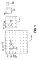
- Fig. 1 shows a series of square texture MIP maps that includes a base map 100 of 8x8 texels. From the base map, each successive map is filtered in size to a smallest size map 108 (i.e., including only one texel). The smallest size map 108 is assigned a map number of zero, and the map number for each successively larger map is incremented by one so that the base map 100 in this example has a map number of three. The map number is used in determining the block tag for each block of texture data in a manner that is described below.
- a map number of ten corresponds to a map of 1024x1024 texels
- a map number of nine represents a 512x512 texel map
- a map number of eight represents a 256x256 texel map
- the texture base map is not square, then a map number often corresponds to a map having a larger dimension of 1024 texels. While this discussion assumes a square texture base map, rectangular maps also are possible. If rectangular, the map number is determined by the number of texels of the longer dimension of the map. For example, a rectangular map having a map number of ten has a longer dimension with 1024 texels. It also should be understood that other map numbering schemes can alternatively be used.
- a square 1024x1024 texel map that has a map number often requires ten bits of S coordinates S[9:0] and ten bits of T coordinates T[9:0] to uniquely identify the location of each texel within the map.
- a map having a map number of nine requires nine bits of both S and T coordinates to identify the location of each texel
- a map having a map number of eight requires eight bits of both S and T coordinates to identify the location of each texel, and so on.
- the S and T coordinates that uniquely identify the location of a texel in a MIP map that correspond to any pixel are interpolated in the manner described above.
- texture data is stored in the main memory 17 of the host computer 15 (Fig. 2) in blocks of 256x256 texels.
- a read cache tag identifying the block of texture data that missed in the cache is read by the host computer, and that block of texture data is then downloaded to the cache memory 48 of the texture mapping board.
- sixty-four blocks of texture data can be stored in the cache memory at any one time. These sixty-four blocks of texture data can include data from multiple MIP maps of one or more textures. Each block has an associated block tag that uniquely identifies it. MIP maps having a map number of nine or larger include greater than 256x256 texels, and therefore are stored in multiple blocks. The high-order S,T coordinates for any map that is stored in multiple blocks are included in the block tag for the blocks of data that store the map.
- MIP maps having a map number of nine have one dimension equal to 512 texels and, if square, are 512x512 texels in size.
- the map is divided into four blocks of 256x256 texels (assuming a square texture map). Therefore, the block tag for each of those blocks includes one high-order S coordinate bit and one high-order T coordinate bit (i.e., S[8] and T[8]) that identify the location of the block within the map.
- MIP maps having a map number often are 1024x1024 texels in size, and are divided into sixteen blocks of data. Therefore, the block tags for each of those blocks includes two high-order S coordinate bits and two high-order T coordinate bits (i.e., S[9:8] and T[9:8]) that identify the location of the block within the map.
- the texture MIP maps are subdivided and stored in memory so that the same portions of adjacent MIP maps are stored in opposite SDRAM banks.
- multiple maps smaller than 256x256 texels can be stored in a single block of cache memory.
- Fig. 12 shows a set of texture MIP maps for a particular texture including the surface image:
- each MIP map in the series of MIP maps for a texture is divided into four quadrants that are of equal size for a square texture map.
- the base map has a map number of nine, and is divided into quadrants 9Q1 (including image L), 9Q2 (including image A), 9Q3 (including image 9) and 9Q4 (including image 5).
- map number eight is divided into quadrants 8Q1, 8Q2, 8Q3, 8Q4, respectively including images L, A, 9 and 5.
- map number seven is divided into quadrants 7Q1, 7Q2, 7Q3, 7Q4 respectively including images L, A, 9 and 5.
- the smaller maps are similarly subdivided into quadrants.
- Two quadrants of each MIP map are stored in one bank of the SDRAMs that form the cache, while the other two quadrants are stored in the opposite bank.
- the texture data allocation scheme of the invention for textures having a base map with a number greater than or equal to eight (being greater than or equal to 256x256 texels in size), the memory locations within the blocks of memory space for all of the quadrants of all of the MIP maps of that texture are predefined. For example, quadrants 9Q1 and 9Q4 of map number nine are stored in separate blocks within cache bank one, and quadrants 9Q2 and 9Q3 are stored within separate blocks of cache bank zero, as shown in Fig. 13. The corresponding quadrants of adjacent MIP maps are stored in blocks within opposite banks.
- quadrants 8Q1 and 8Q4 which respectively include the box filtered texture data of quadrants 9Q1 and 9Q4, are stored in the same block within cache bank zero.
- Fig. 13 is not drawn to scale with respect to Fig. 12. It should be understood that the map quadrants of Fig. 12 are the same size as those of Fig. 13 as they are identical.
- each quadrant of map number nine occupies a complete block of 256x256 texels, whereas the quadrants of map number eight each occupies only 1/4 of a block. Therefore, quadrants 8Q2 and 8Q3 together occupy 1/2 of the same block and quadrants 8Q1 and 8Q4 occupy 1/2 of another block within the opposite bank.
- quadrants 8Q2 and 8Q3 together occupy 1/2 of the same block and quadrants 8Q1 and 8Q4 occupy 1/2 of another block within the opposite bank.
- the unoccupied locations within each of those blocks is occupied by appropriate quadrants of maps having a map number of seven or less. Therefore, all of the maps having numbers zero to eight together occupy two blocks, each of the two blocks being in a separate bank.
- the locations of the quadrants for the maps having map numbers of eight or less are predefined in the manner shown in Fig. 13.
- the upper right quadrant 8Q2 and lower left quadrant 8Q3 maintain the same physical relationship and respectively occupy the upper right and lower left quadrants of a first block
- the upper left quadrant 8Q1 and lower right quadrant 8Q4 also maintain the same physical relationship and respectively occupy the upper left and lower right quadrants of a second block that is in a different bank from the first block.
- quadrants 7Q1 and 7Q4 maintain the same physical relationship and respectively occupy the upper left quadrant of the first block
- quadrants 7Q2 and 7Q3 maintain the same physical relationship and respectively occupy the upper right quadrant of the second block.
- a pixel maps to a position in the texture map that is between four texels in one MIP map and four texels in an adjacent MIP map then all eight texels are accessed from the cache.
- the texels accessed from both MIP maps include common texture data, with the data from the smaller map being a filtered version of the data from the larger map.
- adjacent pixels will frequently map to the same two MIP maps for the texture, requiring that reads to the cache continuously switch between the cache blocks that store the two maps.
- re-paging penalties are not incurred when cache reads switch between the two MIP maps during consecutive read cycles. This provides for efficient implementation of trilinear interpolation.
- a texture when a texture includes a base map having a map number of eight or greater, the allocation of the MIP maps among the blocks for that texture is predefined in accordance with the described illustrative embodiment of the invention. This is so because two quadrants of a map having a map number eight occupy certain predefined locations of a first block within one of the banks, and the other two quadrants of the map having a map number eight occupy certain opposite predefined locations within another block of the opposite bank, as discussed above and shown in Fig. 13.
- multiple locations within the two blocks of memory are available to store the maps, and are selected by the host computer.
- a sub-texture identification is assigned in a manner described below to identify the location of each map within the shared block.
- Fig. 13 shows the manner in which a second series of MIP maps from a different texture (i.e., a checkerboard pattern) is allocated among the memory blocks.
- the MIP maps of this second texture are subdivided and stored in separate blocks of data in the same manner as the first texture.
- the organization of Fig. 13 shows the MIP maps of the different textures as being organized in separate blocks, it should be understood that texture data from two different textures can be stored within the same block.
- the cache memory can store up to sixty-four blocks of texture mapping data, with each block including 256x256 texels.
- the cache memory is divided into two banks, with blocks 0-31 lying in bank zero, and blocks 32-63 lying in bank one.
- the cache directory includes up to sixty-four block tag entries that correspond to the blocks in the cache.
- the physical location of each block tag within the cache directory identifies the physical location of the corresponding block of texture data within the cache memory.
- a block index is generated from the block tag that indicates the location of the block.
- the cache address for any texel in the cache is formed from the block index for the block, and the texel address within the block.
- the texel address includes the low-order interpolated S,T coordinates for the texel, and may also include bits from the sub-texture ID as discussed below.
- Fig. 14 shows an example of a texture MIP map having a map number of nine that is subdivided into quadrants.
- the MIP map is 512x512 texels in size; and therefore, each quadrant is 256x256 texels in size and corresponds to a single block of memory.
- a simple scheme is implemented by the host computer to determine the bank in the cache to which each quadrant of the MIP map should be assigned.
- the results of a logical exclusive OR operation on the values of the most significant bits of the S and T coordinates for the quadrant dictate the SDRAM bank in the cache to which the quadrant is assigned.
- nine S coordinate bits S[8:0] and nine T coordinate bits T[8:0] specify the location of each texel within the map.
- the quadrant boundaries are established at the halfway point of the map in both the S and T dimensions, represented by the most significant S and T coordinate bits S[8] and T[8]. Therefore, to determine the cache banks for each of the four quadrants of a MIP map having a map number of nine, an exclusive OR operation is performed for each quadrant on the values of its corresponding most significant S and T coordinate bits S[8] and T[8].
- the cache bank for each quadrant is determined by an exclusive OR operation on the corresponding values of its most significant S and T coordinate bits S[9] and T[9].
- the result of the exclusive OR operation is inverted so that common data from adjacent maps are stored in different banks.
- the blocks labeled block1-block4 correspond respectively to the upper left quadrant, the upper right quadrant, the lower left quadrant and the lower right quadrant of the 512x512 texel map.
- bits S[8], T[8] are respectively equal to [0,0], [1,0], [0,1] and [1,1]. Therefore, for blockl the result of the XOR operation S[8] XOR T[8] equals zero. Because the map has an odd map number (i.e., nine), the inverse of this result (equaling one) is used to indicate that blockl is to be stored in bank one of the cache.
- the inverse of the result of the XOR operation S[8] XOR T[8] equals zero, indicating that block2 is to be stored in bank zero in the cache.
- the inverse of the result of the XOR operation S[8] XOR T[8] respectively equals one and zero indicating that block3 is to be stored in bank one and block4 is to be stored in bank zero.
- the map would be split into sixteen blocks of 256x256 texels each, because the map is 1024x1024 texels in size.
- the results of S[9] XOR T[9] would indicate the bank number for that particular block. Note that the result of the XOR operations for each block of the map having a map number often are not inverted as they were for the adjacent map having a map number nine, so that the corresponding quadrants in the two maps are stored in different cache banks.
- the block tag for blocks of texture data that represent the map may include at least one high-order S coordinate bit and one high-order T coordinate bit that indicates the location of the block within the particular MIP map.
- S coordinate bit and one T coordinate bit For a 512x512 texel MIP map having a map number of nine, only one S coordinate bit and one T coordinate bit would be required in the block tag to indicate the location of each block within the MIP map.
- 1024x1024 texel MIP map having a map number of ten and including sixteen blocks of data two S coordinate bits and two T coordinate bits would be required in the block tag to indicate the location of each block within the MIP map.
- no S and T bits are required in the block tag.
- each block of data can be further subdivided into sixteen sub-blocks of 64x64 texels.
- Each sub-block of texture data includes a sub-texture ID that identifies the location of the particular sub-block within the block.
- the sub-texture ID includes two S bits S[1:0] and two T bits T[1:0].
- Multiple sub-textures from one or more MIP maps of one or more textures can be stored in a single block.
- Fig. 15 illustrates block1 and block2, respectively assigned to banks zero and one of the cache, each sub-divided into sixteen sub-textures of 64x64 texels in size.
- the sub-textures of each block are labeled ST0-ST15, and are identified by a sub-texture ID that includes two S coordinate bits and two T coordinate bits.
- the sub-textures have consistent labeling but mirror locations within the two cache banks to be consistent with the memory allocation scheme described above.
- the size of the sub-textures of 64x64 texels is selected to be exemplary and can be altered. For example, a smaller sub-texture would enable more textures to be packed within the same blocks. It should be understood that the sub-texture ID would need to include more bits as the size of the sub-texture is decreased.
- the texture ID, sub-texture ID and 8-bit word representing the size of the base map for that texture associated with those texels is provided through the 3-D pipeline to the tiler/boundary checker which temporarily stores the data in a 20-bit register (not shown).
- the tiler/boundary checker which temporarily stores the data in a 20-bit register (not shown).
- the new data is provided to the tiler/boundary checker and stored in the register.
- the sub-texture ID may be used as part of the texel address, as explained below.
- Whether the texel address includes S,T coordinate bits of a sub-texture ID depends on the size of the map being addressed and the size of the base map of that texture. If the map being addressed has a map size of seven or smaller and its corresponding base map is also of size seven or smaller, then certain upper address bits of the texel address include bits from the sub-texture ID to address the location of the sub-texture within the block, as explained in detail below. As explained above, when the base map has a map number of eight or greater, the locations of all of the MIP map quadrants for that texture within their respective blocks of data are predefined.
- the texture address for each map includes sub-texture ID bits. For example, if four different maps having map numbers of seven from four different textures are allocated among different sub-textures within a block, and the map number for the base map of each texture is seven, then one S coordinate bit and one T coordinate bit from the sub-texture ID would be part of the texel address to distinguish between the textures.
- the routine by which the tiler/boundary checker computes the texel address is described below with reference to Fig. 17.
- texture MIP map data is downloaded one block at a time.
- a sub-texture ID can be included in the block tag so that sub-textures could be downloaded from the main memory.
- the sizes of the blocks and sub-textures described in this embodiment are intended solely to be exemplary and can be altered to suit any application.
- the cache directory includes a block tag for each of its sixty-four entries, and identifies a corresponding block index for each entry.
- the block index identifies the physical location in the cache where the beginning of the corresponding block of texture data is stored.
- the block tag is a 23-bit identifier that uniquely identifies each block of texture data in the manner shown in Fig. 16.
- the texture mapping hardware supports an 8-bit texture ID that uniquely identifies a texture. Additionally, for texture data from different textures stored within the same block, an additional 4-bit sub-texture ID is supported by the hardware to identify the textures.
- the texture mapping hardware of the present invention supports 2 12 or four thousand ninety-six unique textures that can be active at any one time.
- each texture is represented by a series of MIP maps, and in one embodiment of the invention, each of the MIP maps is provided with a map number indicating its position in the series of MIP maps.
- any texel of data is identified not only by the texture ID, sub-texture ID, and size of the base map for that texture, but also by the map number of the MIP map to which it corresponds.
- the texel is uniquely identified within the MIP map by its S and T coordinates (i.e., its interpolated S,T value).
- the above-described parameters that uniquely identify a texel are used to generate the 23-bit block tag.
- the hardware used to generate the S and T coordinates is limited to fifteen bits. Therefore, for this embodiment, the largest texture map supported by the hardware has a 15-bit S field [14:0] and a 15-bit T field [14:0], resulting in a maximum texture map that is 32Kx32K texels in size.
- each block of texel data includes 256x256 texels.
- the low-order S and T bits i.e., T[7:0] and S[7:0]
- T[7:0] and S[7:0] are used to identify a particular texel within a block of texel data.
- the high-order S and T bits are used in the block tag to identify a particular block of texel data.
- each MIP map is assigned a map number uniquely identifying it within the series of maps for its corresponding texture. Irrespective of the number of MIP maps in the series of maps for a texture, the smallest MIP map in the series (i.e., one texel in size) is assigned to be map number zero. Since the largest series of MIP maps for a 32Kx32K texture includes sixteen MIP maps, the largest map number supported is fifteen.
- Block tag [14] corresponds to a map bit that in conjunction with the values in the high-order T coordinate field, enables the identification of the map number. It should be understood that maps smaller than the maximum 32Kx32K do not employ the full S and T address fields, such that the smaller the map, the more high-order S and T address bits that are unused. As shown in Fig.
- the block tag bit corresponding to the least significant unused T coordinate bit is set to logical "0"
- the block tag bits corresponding to the remaining high-order T coordinate bits and the map bit are set to logical "1”.
- the map bit is set to logical "0".
- Block tag bit [07] represents in which of the two blocks each one-half portion of the maps having map numbers of eight and less is stored.
- the block tag bit [07] has a value of "0" for the one-half (two quadrants) of that map (that is stored in the bank zero block) and has a value of "1" for the other one-half (two quadrants) of that map (that is stored in the bank one block). It should be understood that because all of the maps from a particular texture having a map number of eight or less are stored within two blocks, then only one block tag bit is used to identify those two blocks. The particular map number for each of the maps having a number eight and lower therefore is not stored as part of the block tag field.
- the value of block tag bit [07] for each quadrant of each of the maps having a map number of eight or less is computed based on the scheme for determining the bank in which the quadrant should be stored.
- This scheme includes the logical exclusive OR operation of the values of the MSB bits for each quadrant of even numbered maps and the inverse of the operation for each quadrant of odd numbered maps.
- the block tag bits [6:0] that correspond to the high-order S address bits are set to logical "0" for small maps when the S address bits are unused, so that if any of these bits is detected as a logical "1" in conjunction with a map number indicating that they should be equal to a logical "0", it can be used to indicate that there is no valid data included in the cache directory entry.
- each MIP map quadrant the results of a logical exclusive OR (XOR) operation on the values of the most significant S and T coordinates for the quadrant dictate the SDRAM bank in the cache to which the quadrant is assigned.
- the bank number is equal to this XOR operation for maps having an even map number, and is equal to the logical inverse of the XOR operation for maps having an odd map number. This is shown in the right-hand column of the table of Fig. 23, wherein the symbol " ⁇ " indicates an XOR operation, and the symbol "! indicates a logical inverse.
- each quadrant consumes at least one full block of data, and each block is stored in the bank dictated by the XOR operation shown in the last column of the table of Fig. 16.
- the block tag bit [07] represents in which of the bank zero block or bank one block the half map is stored. The value of that bit [07] is computed based on the XOR operation described. For example, for a map having a map number eight, for each quadrant of the map, the block tag bit [07] would equal S[7] XOR T[7]. For each quadrant of a map having a map number seven, the block tag bit [07] would equal the inverse of S[6] XOR T[6].
- the block tag bit [07] is similarly computed for each quadrant of smaller maps with the result of the XOR operation being inverted for odd numbered maps only. It should be appreciated from the foregoing that because two quadrants of each map (having a map number of eight or less) are stored in the same block, those two quadrants of each map would have the same block tag bit [07].
- the cache directory When a hit occurs between interpolated S,T coordinates (addressing a texel to be accessed) and one of the 23-bit block tags in the cache directory, the cache directory generates a block index indentifying the physical location in the cache memory where the cache block containing that texel is stored.
- the texel address is a 16-bit word including bits S[7:0] and T[7:0] that indicates the location of the texel to be accessed within the 256x256 texel block.
- the texel address is computed from the interpolated S,T coordinates, the map number of the map to be accessed, the texture and sub-texture IDs, and the base map size of the texture, in accordance with a routine discussed below with reference to Fig. 17.
- the LSB S bit and LSB T bit of the texel address are decoded to determine the appropriate interleave in which the texel is stored.
- the remaining fourteen bits of the texel address in conjunction with the six block index bits serve as the cache address (with the six bits of the block index being the six MSBs of the cache address) provided to the SDRAM pair within the decoded interleave of the cache.
- the tiler/boundary checker element 72 receives from the parameter interpolator 64 the interpolated S,T value of the texel to be accessed as well as a 4-bit word that represents the map number of the map from which the texel should be accessed.
- Each of the interpolated S and T coordinate values received from the parameter interpolator includes sixteen integer bits and eight fractional bits.
- the 4-bit word representing the map number includes maps ranging from map number zero (one texel in size) to map number fifteen (32kx32k texels in size) and is computed from the gradient, as described above.
- a comparison of the interpolated S,T value with the block tag entries in the cache directory then is performed. If a hit occurs with one of the block tags, then the block index is generated.
- the texel address is computed in accordance with the routine described below with reference to the flowchart of Fig. 17.
- the texel address is computed by the tiler/boundary checker based on the texture ID, sub-texture ID, map number, base map number and interpolated S,T coordinates of the texel.
- the tiler boundary checker has all of this information. For each unique texel to be accessed, the tiler/boundary checker receives from the parameter interpolator the interpolated S,T coordinates (including sixteen integer and eight fractional bits for each of S and T) as well as a 4-bit word representing the map number from which the texel is to be accessed.
- a command including the 8-bit texture ID, the 4-bit sub-texture ID and an 8-bit word representing the size of the base map for that texture.
- the 8-bit word that represents the size of the base map includes four S bits and four T bits which correspond to the map numbering scheme of the invention and respectively define the size of the S dimension and T dimension of the base map.
- each of the 4-bit S and T words can have a value ranging from zero (which corresponds to a dimension of one texel) to fifteen (which corresponds to a dimension of 32k texels).
- the twenty bits of data including the texture ID, the sub-texture ID and base map number are temporarily stored in a 20-bit register (not shown) within the tiler/boundary checker until replaced with new and different data for a subsequent texel to be accessed from the cache. With this information, the tiler/boundary checker computes the texel address for each texel.
- each bit of the texel address for any texel of such a texture can be computed in accordance with this known predefined allocation scheme.
- the routine implemented by the tiler/boundary checker to compute the texel address is illustrated by the flowchart of Fig. 17.
- the routine requires one cycle to complete.
- the routine may be implemented by a set of logic gates (not shown) that form the boundary checker portion of the texture mapping chip. It should be appreciated by those skilled in the art how to implement the logic gates to perform the routine outlined by the Fig. 17 flowchart.
- the routine can be written in a software simulation language such as Verilog, and then converted into a logic gate circuit by a synthesis tool such as SynopsysTM operating on a general purpose processor.
- the routine alternatively can be written in software and performed by a processor.
- the routine starts at step 250 where the texel address bits S[7:0], T[7:0] are preset to be equal to the interpolated S,T coordinate bits S[7:0], T[7:0]. Each of the bits of the texel address will remain at the value to which it is preset (equal to the corresponding S or T coordinate) in this step unless reset later in the routine. Then the routine proceeds to step 252 where it is determined whether the particular map within which the texel being interpolated is stored has a map number of greater than or equal to eight. If so, then the routine ends for such a texel and the bit values for the texel address remain as preset equal to the interpolated S,T coordinates.
- step 254 it is determined whether the texel is stored in bank number one or bank number zero. As described above, it is known whether the texel is stored in bank number one or bank number zero by examining the value of block tag bit [07].
- step 268 it is determined whether the base map has a map number equal to seven. If so, then the routine proceeds to step 270 where it is determined whether the texel is stored in bank zero or one.
- texel address bit S[7] equals the inverse of the subtexture ID bit S[1] and texel address bit T[7] equals subtexture ID bit T[1] and, for maps having map numbers zero to six, texel address bits S[7:6] equal the inverse of subtexture ID bit S[1] and 1, respectively, and texel address bit T[7] equals subtexture ID bit T[1].
- the routine then ends for such a texel.
- step 274 If the texel is stored in bank zero, then the routine proceeds to step 274 where, for a map having a map number seven, texel address bit S[7] equals subtexture ID bit S[1] and texel address bit T[7] equals subtexture ID bit T[1] and, for maps having map numbers zero to six, texel address bits S[7:6] equal subtexture ID bit S[1] and 0, respectively, and texel address bit T[7] equals subtexture ID bit T[1]. The routine then ends for such a texel.
- step 260 If the base map of the texture does not have a map number greater than or equal to eight (determined in step 260), nor a map number equal to seven (determined in step 268), then it is of course known that the base map of the texture has a map number less than or equal to six and the routine proceeds to step 276 where it is determined whether the texel is stored in bank zero or bank one. If the texel is stored in bank one, then the routine proceeds to step 278 where the texel address bits S[7:6] are set equal the inverse of the subtexture ID bits S[1:0] and texel address bits T[7:6] are set equal the subtexture ID bits T[1:0]. The routine then is complete for such a texel.
- step 280 the routine proceeds to step 280 where the texel address bits S[7:6] equal the subtexture ID bits S[1:0] and texel address bits T[7:6] equal the subtexture ID bits T[1:0]. The routine is then complete for such a texel.
- a primitive A to be rendered may map to a texture A
- a primitive B may map to a texture B.
- One possibility would be for the host computer to organize texture A into a plurality of blocks of texture data, and then organize texture B into different sub-textures within the same blocks as texture A.
- the host computer would download the blocks of texture data including textures A and B into the cache memory before rendering primitives A and B.
- the host can organize texture A into a plurality of blocks of texture data, and then download the blocks including texture A into the cache memory.
- the host computer could then organize texture B in the main memory within different sub-textures in the same blocks as texture A.
- the host computer would issue a command to halt the operation of the texture mapping chip 46 (Fig. 2), and would download the newly organized blocks of texture data (including textures A and B in the same blocks) to the cache memory of the texture mapping system.
- the HALT condition were not implemented and the newly organized data from the main memory were not downloaded into the cache memory of the texture mapping system, false texture mapping data could be accessed during the rendering of primitive B.
- one feature of the present invention enables a MIP map for a new texture to be downloaded to the local memory in the texture mapping hardware through a data path that is separate from the pipeline for handling 3-D primitive data.
- the texture mapping board 12 (Fig. 2) and the texture mapping chip 46 (Fig. 3) each has separate ports for respectively receiving 3-D primitive data and texture data.
- the 3-D primitive data is received from the concentrator chip 36 via bus 18, whereas the texture data is received from the 2-D geometry accelerator chip 34 via bus 24.
- the 3-D primitive pipeline through the front end board 10 and the texture mapping chip 46 need not be flushed, thereby providing increased bandwidth when compared with conventional texture mapping systems which require a flushing of the 3-D primitive pipeline whenever new texture data is downloaded to the local memory in the texture mapping hardware.
- the separate data path for downloading texture data that bypasses the 3-D primitive pipeline is particularly beneficial in connection with the above-described embodiment of the present invention wherein the local memory on the texture mapping board 12 is implemented as a cache.
- the local memory on the texture mapping board 12 is implemented as a cache.
- the texture mapping board 12 is provided with two texture mapping chips 46A and 46B, and two cache memories 48A and 48B.
- both cache memories 48 maintain the same texture data at all times, because both of the two texture mapping chips typically operate simultaneously on primitives using the same texture data. Therefore, by updating both caches anytime a miss is received from one, this embodiment of the present invention conserves system bandwidth by ensuring that the same texture data need not be downloaded in separate operations to the two caches.
- each cache memory is updated only with texture data downloaded from the host computer, and is not written locally from the texture mapping hardware. Therefore, consistency between the two cache memories is maintained by ensuring that whenever texture data is downloaded from the host computer in response to a miss from one of the caches, both caches are updated with the new texture data.
- both texture mapping chips 46 are halted so that both cache memories can be updated with the downloaded texture data.
- each texture mapping chip is responsive to the generation of a cache miss signal from any of the texture mapping chips to halt operation.
- the present invention supports simultaneous cache misses from the two texture mapping chips 46 to different cache blocks, and responds by downloading both new blocks of texture data to both caches in response to the misses.
- the bypassing of the3-D primitive pipeline is accomplished by employing the 2-D primitive pipeline through the 2-D geometry accelerator chip 34 to download texture data.
- the data path for downloading texture data to the texture mapping chip 46 can be implemented in a number of alternative ways while still bypassing the 3-D primitive pipeline.
- a dedicated data path can be provided from the host computer to the texture mapping board.
- the host computer of the graphics system of the present invention may employ an operating system, such as UNIX, that can have multiple processes operating simultaneously, and that provides some scheme for allowing a process to lock certain system resources, such that a process cannot be interrupted when locked.
- an operating system such as UNIX
- UNIX an operating system
- a process that uses certain hardware resources can ensure that the process will not be swapped out until it unlocks those resources.
- two types of locks are provided for use by processes, i.e., fast lock and slow lock.
- a fast lock is employed, a process being swapped in checks the appropriate hardware resources to determine whether it was the last process to use those resources. If it was, then the process simply continues without restoring the state of the hardware resources. However, if the process was not the last one to use the resources, then a slow lock is requested, which results in the restoration of the hardware resources to the state they were in when the process was last swapped out. It should be understood that a number alternative techniques can be employed to achieve the same results.
- Some processes perform both 3-D and 2-D operations, and may switch between 3-D primitives and 2-D primitives without giving up the slow lock. Such processes also implement a scheme for ensuring that the 3-D pipeline is empty before downloading 2-D primitive data to the hardware, and similarly ensuring that the 2-D pipeline is empty before downloading 3-D primitive data. To accomplish this result, register status bits may be provided that indicate whether each of the 2-D and 3-D primitive pipelines is empty. Any process that employs both 2-D and 3-D primitive data reads this status register to ensure that the pipelines are empty before switching between 2-D and 3-D primitive data.
- the illustrative embodiment of the invention disclosed in the figures includes a local memory on the texture mapping board that is implemented as a cache, the invention is not so limited.
- the texture mapping system can alternatively be implemented so that the local memory on the texture mapping board is not a cache, and other techniques are employed to ensure that each block of texture mapping data needed to render a primitive is downloaded, through a path separate from the 3-D primitive pipeline, before the primitive is rendered, so that the texture mapping data is available from the local memory when the primitive is rendered.
- the scheme of the present invention for generating an interrupt to a host computer to update blocks of data in a local memory can be used with many other applications, and is not limited to use in a texture mapping hardware system.
- This scheme is useful in any data processing system that includes a host computer with a main memory that stores blocks of data to be processed, and data processing hardware having a local memory that stores blocks of data being processed.
- the first set of registers includes two 32-bit most recently used registers MRU0 and MRU1 (collectively MRU), which respectively correspond to banks zero and one of the cache 48. Each bit in these registers corresponds to one of the thirty-two cache blocks contained within its corresponding cache bank. Each time a hit occurs to a block in the cache, the corresponding bit in MRU0 or MRU1 is set so that the most recently used registers accumulate hits for the cache.
- step 306 the method deasserts the bits in BLOCKS_TO_USE that correspond to the bits asserted in either MRU or CU.
- a logical OR of the MRUs and CUs is used to determine which bits in BLOCKS_TO_USE are deasserted.
- step 308 a determination is made as to whether any bits are asserted in BLOCKS_TO_USE, and when at least one is, the method proceeds to step 310, wherein a determination is made as to whether the number of asserted bits in BLOCKS_TO_USE is below a predetermined threshold. This step is performed to assist in the maintenance of a history of cache block usage over multiple cache misses, and to ensure the proper handling of future cache miss interrupts in the manner discussed below.
- the method proceeds to step 312, wherein all of the bits in the MRUs are deasserted.
- the pipe tag register stores the last block tag that was indexed by the pipeline in the texture mapping chip.
- the pipe tag register stores the block tag 370 that missed in the cache.
- the caches in each are maintained to have identical entries. Therefore, texture data downloaded from the host computer in response to a cache miss from one of the texture mapping chips is written to the caches in both chips.
- the method proceeds to step 410 wherein the cache address register in Loki0 and Loki1 (if Loki1 exists) is written with the block index determined during step 408.
- the directory tag register is written with the block tag of the block of texture data to be downloaded to the texture cache in response to the cache miss
- the texture data is written to the texel data register. In this manner, the method responds to the cache miss by downloading the block of texture data missed in the cache and writing this block of data to the cache.
- the method will determine at step 416 whether Loki1 has interrupted, and if it has not, will also proceed directly to step 418 wherein the halt bit will be deasserted in both texture mapping chips, allowing them to proceed with processing primitives. However, when it is determined at step 416 that Loki1 has interrupted in response to a cache miss, the method proceeds through steps 420-424 to process the interrupt in the same manner as was discussed in connection with steps 406-414 for handling the interrupt from Loki0. The method then proceeds to step 418 wherein the halt bits in both texture mapping chips are deasserted.
- both chips can generate a cache miss interrupt simultaneously for the same block tag, or for different block tags.
- the interrupt will be processed in steps 400-414. Therefore, in step 416, the method will not detect an interrupt from Loki1, because the interrupt from Loki1 will be cleared by the writing of the missed block tag to the directory tag register of both Lokis in step 412.
- the method shown in Fig. 20 is capable of responding to an interrupt from either texture mapping chip individually, or from both simultaneously.
- the cache system of the present invention includes both a mini-directory (Fig. 21) and a main directory (Fig. 22).
- the mini-directory is fully associative and includes the five most recently read cache block tags, as well as a corresponding block index for each.
- the mini-directory 500 includes five entries that are respectively output from the mini-directory over outputs 501-505, each of which is coupled to four groups of tag comparators 507-510.
- Each group of tag comparators 507-510 includes five 23-bit comparators (not shown), and corresponds to one of the four cache read tags performed in a single read operation when performing bilinear or trilinear interpolation.
- the fully associative nature of the mini-directory is implemented with twenty 23-bit comparators, equal to the number of tags simultaneously read, multiplied by the number of entries in the mini-directory.
- Each group of tag comparators 507-510 compares its corresponding cache read tag against the five block tags stored in the mini directory, and produces a hit output indicating whether the tag matches one of the mini-directory entries, and when it does, also outputs a block index indicating the location in the cache wherein the corresponding block of texel data is stored.
- the comparators include comparator 526 that compares the UL tag against the UR tag, comparator 527 that compares the UL and LL tags, comparator 528 that compares the UL and LR tags, comparator 529 that compares the UR and LL tags, comparator 530 that compares the UR and LR tags, and comparator 532 that compares the LL and LR tags.
- comparators 526-532 can be performed in parallel with other comparisons so as to not incur any performance penalty. For example, these comparisons can be performed during the cycle when the cache read tags are compared to the mini-directory, or during the cycle when a first cache read tag that missed in the mini-directory is compared to the main directory. When it is determined that at least two cache read tags do not hit the main directory and are equal, the outputs of comparators 526-532 are used to indicate that the main directory need only be accessed once for these at least two cache read tags. In this manner, multiple cycles need not be incurred in accessing the main directory for tags that are identical, thereby minimizing the impact on system bandwidth when two or more cache read tags miss the mini-directory.
- the mini-directory stores five block tags to ensure that even if four unique cache tags for a currently processed set of read tags is resident in the mini-cache, at least one tag accessed in the previous set of read tags will remain in the mini-directory. Thus, even when switching between two sets of four unique cache tags during trilinear interpolation, at least one of the read cache tags for each set will remain in the mini-directory so that four cache tags will not need to be compared against the main directory in a serial fashion.
- consecutive reads to the cache will read a first set of four texels in one map, and a second set of four texels in another.
- adjacent texels within each of two maps will each be accessed every other cycle, and two or more of the texels will generally be located within a single cache block. Therefore, if only one or two unique tags appear in each set of four cache read tags, a large number of pixels can be rendered with each cache read tag hitting the mini-directory 500. If only one cache read tag in each set of four misses the mini-directory, no performance penalty is incurred because that tag can be compared against the main directory while the next set of four read tags is being compared to the mini-directory.
- the performance penalty incurred to achieve this hardware savings is application dependent, based on the behavior of the sequence of tags accessed in consecutive read operations. If no more than one tag in each read set misses the mini-directory, no penalty is incurred as the missed tag can be compared against the main directory in parallel with the next set of read tags being compared against the mini-directory.
- comparators 526-530 that are used to reduce performance penalties when two or more cache read tags miss in mini-directory, six are used because four read tags are accessed simultaneously.
- the number of comparators employed to compare each cache read tag against the others is dependent upon the number N of read tags accessed simultaneously, and is equal to a summation of integers from one through N-1.
- each of registers 550-553 is also coupled to a control circuit 559 that receives the outputs of the mini-directory tag comparators 542-546.
- each of registers 550-553 is also loaded with data identifying whether its corresponding tag (i.e., UL, UR, LL, LR) matched one of the mini-directory entries, and if so, which entry was matched.
- a sixth comparator 541 is used to compare the four read tags (UL, UR, LL and LR) against the tag that missed in the mini-directory in the previous cycle and is being compared against the main directory. If more than one unique tag in the set of four cache read tags (UL, UR, LL and LR) misses the mini-directory, the pipeline through the cache directory is halted because multiple comparisons will occur with the main directory. However, if only one unique tag misses the mini-directory, the pipeline continues in the following manner so that the cache directory receives a new set of four cache read tags each cycle.
- the read tags that were compared against the mini-directory in the previous cycle are stored in registers 550-553.
- the outputs of these registers are coupled to a four-to-one multiplexer 555, which selects one of those registers at a time to be compared against the main directory, and to be loaded into the mini-directory at the end of the cycle so that the mini-directory is updated with the most recently received read cache tags.
- the output of multiplexer 555 is also coupled to the sixth comparator 541, so that the cache read tag that missed the mini-directory in the preceding cycle is compared against each of the new set of read tags UL, UR, LL and LR.
- comparator 541 ensures that the mini-directory compares each set of four cache read tags received by the cache directory against the five most recently received read tags.
- the set of six comparators 526-532 discussed above in connection with Fig. 23 is shown as a single comparator block in Fig. 24 for convenience.
- the outputs of these comparators, as well as the outputs of comparators 541-546, each is provided to control circuit 559, which performs several functions.
- the control circuit 559 determines which entry in the mini-directory is to be replaced with the new read cache tag.
- the control circuit 559 does not replace any entry that was hit by one of the four newly received read cache tags being compared against the mini-directory, or the last read cache tag compared against the main directory, and assigns these entries a highest priority for being maintained in the mini-directory.
- the control circuit 559 stores state information regarding which mini-directory entries where hit by the preceding set of four read tags, and assigns them the next highest priority for being maintained in the mini-directory. The remaining entries are assigned a lower priority.
- the five mini-directory entries are labeled one through five.
- the entry to be replaced is selected from the lowest priority group by first identifying the highest number entry that is not in the group, and then selecting for replacement the next highest number entry that is in the group.
- the scheme wraps around so that entry one is treated as the next highest number entry.
- the control circuit 559 cycles through the mini-directory entries each time one must be replaced, and controls the loading of the selected mini-directory tag register 501T-505T.
- the control circuit 559 also decodes the outputs of comparators 541-546 to generate data for each of the four read tags (UL, UR, LL and LR) indicating whether the read tag matched an entry in the mini-directory, and if so, which entry was matched. This data is stored in the corresponding register 550-553 for each of the read tags UL, UR, LL and LR. For example, if the read tag UL matched mini-directory Entry3, the data decoded by the control circuit 559 would be stored in the UL register 550 to indicate that read tag matched mini-directory Entry3.
- each of the registers 550-553 that stores that read tag is loaded with data indicating that the block index for the corresponding texture data is not in the mini-directory.
- the output of one of registers 550-553 that stores the missed tag is compared against the main directory 520, and the block index for the read tag is loaded from the main directory into a register 561 that stores the main directory block index.
- the data indicating that the block index does not correspond to any entry in the mini-directory is also stored in the register 561 from input 562 that is provided from the output of multiplexer 555.
- the cache memory includes four interleaves A-D so that four texels can be accessed simultaneously.
- the set of four texel read tags UL, UR, LL and LR can correspond in any manner to interleaves A-D.
- the data stored in registers 550-553 that identifies which mini-directory entry stores the block index corresponding to each of texels UL, UR, LL and LR is passed through a barrel shifter 563, which is controlled to correlate each of texels UL, UR, LL and LR to its corresponding interleave A-D.
- interleave index control registers 565-568 which respectively correspond to interleaves A-D, and which each identifies the mini-directory entry, if any, that stores the block index for the interleave.
- the main directory 520 is only accessed once to provide the block index for that read tag. This process is also controlled by control circuit 559, which uses the outputs of comparators 526-532 to identify whether any two of the four read tags match. If two or more of the set of four read tags miss the mini-directory but include the same cache tag, each of the corresponding registers 550-553 is set by control circuit 559 to indicate that the block index is not included in any mini-directory entry. Thus, when the data corresponding to those read tags is passed into interleave index registers 565-568, each will select the main directory block index control register 561 to be passed through its corresponding interleave index multiplexer 571.
- the control circuit 559 also sets a directory control register 573 that controls which of read tag registers 550-553 is to be compared against the main directory.
- the register 573 controls the multiplexer 555 to select one of the registers 550-553 to be compared against the main directory at a time. If more than one of the read tags UL, UR, LL, LR misses the mini-directory but share a common tag, the control register 573 is set to indicate that only one of the registers should be compared against the main directory. In this manner, the main directory is accessed only once when the set of four read cache tags includes only a single unique tag that misses the mini-directory.
- the missed tags are processed serially.
- the control circuit 559 determines which entry in the mini-directory is to be replaced by a first missed read tag, and the corresponding register 550-553 is loaded with data indicating that its block index will be stored in that mini-directory entry.
- the main directory block index register 561 is updated with the data indicating which mini-directory index register 501I-505I is to be replaced.
- the corresponding block index is loaded from the register 561 into the register 501I-505I that corresponds to the mini-directory entry selected for replacement.
- Each of the subsequently processed unique tags that missed the mini-directory is handled in the same manner until the last miss tag to be processed, which can be a second miss tag if only two unique tags missed the mini-directory, or can be a third or fourth miss tag.
- the last miss tag processed through the cache directory is handled as if it were the sole unique tag in the set of read tags to miss the mini-directory.
- the directory deasserts the signal indicating that it is busy so that it can receive a new set of read tags.
- the control circuit 559 loads its corresponding register 550-553 with data indicating that the block index for the tag is not stored in any mini-directory entry. This can be done during the first cycle wherein all the read tags are compared against the mini-directory, or in parallel with the processing of the other miss tags.
- the data in registers 550-553 is passed through the barrel shifter 563 and loaded into interleave control registers 565-568, and the block index for the miss tag is loaded from the main directory into the main directory block index register 561.
- the outputs of the interleave index control registers 565-568 are used to control their corresponding interleave index multiplexers 571, so that the index for the last processed miss tag is provided from the main directory block index register 561, and the block index for each of the other read tags in the set is provided from its corresponding mini-directory index register 501I-505I. It should be understood that by accessing the block index for the last processed miss tag from the main directory block index register 561, a cycle is saved by not waiting for the block index for this tag to be loaded into its mini-directory index register.
Landscapes
- Engineering & Computer Science (AREA)
- Theoretical Computer Science (AREA)
- Physics & Mathematics (AREA)
- General Physics & Mathematics (AREA)
- General Engineering & Computer Science (AREA)
- Computer Graphics (AREA)
- Image Generation (AREA)
- Memory System Of A Hierarchy Structure (AREA)
Claims (10)
- Procédé pour allouer des données de texture (S, T) entre au moins une première (BANK0) et une deuxième (BANK1) zone d'une mémoire accessible séparément dans un système d'infographie à mappage de texture, lesdites données de texture comprenant au moins une série de cartes MIP de texture (figure 12 : MAP9, MAP8, MAP7) représentant une texture, dans lequel chaque carte d'une série est une version filtrée d'une carte adjacente, de manière à fournir des cartes successives de taille réduite et lesdites zones de mémoire pouvant être allouées par blocs d'emplacements de texels, le procédé comprenant les étapes consistant à :diviser chaque carte en au moins deux parties de carte (figure 13 : 8Q1, 8Q4 ; 8Q2, 8Q3) ; etallouer les parties de carte de chaque carte dans lesdits blocs de telle sorte qu'une partie (8Q1, 8Q4) d'une carte soit mémorisée dans un bloc à l'intérieur de la première zone de mémoire (BANK0) et l'autre partie (8Q2, 8Q3) soit mémorisée dans un bloc à l'intérieur de la deuxième zone de mémoire (BANK1) de façon que les parties ayant des données de texture communes par rapport aux cartes adjacentes soient mémorisées dans des blocs de zones de mémoire différentes.
- Procédé selon la revendication 1, dans lequel lesdites zones de mémoire peuvent être allouées en blocs de tailles égales d'emplacements de texels.
- Procédé selon la revendication 1, dans lequel l'étape de division comprend l'étape consistant à diviser chaque carte en quadrants (Q1, Q2, Q3, Q4).
- Procédé selon la revendication 1, comprenant en outre l'étape consistant à :affecter une marque de bloc à chaque bloc pour identifier une carte particulière mémorisée dans le bloc, une partie de la carte mémorisée dans le bloc et une texture de la carte mémorisée dans le bloc.
- Procédé selon la revendication 1, comportant en outre les étapes consistant à :subdiviser chaque bloc en une pluralité de texture secondaire et allouer les textures secondaires (ST0-St15) à l'intérieur des espaces inutilisés des blocs (block1 - block4).
- Mémoire (48, 48A, 48B) pour enregistrer des données de texture (S, T) dans un système d'infographie de mappage de texture, les données de texture comprenant au moins une série de cartes MIP de texture (figure 12 : MAP5, MAP9), chacune de ces séries représentant une texture, où chaque carte d'une série est une version filtrée d'une carte adjacente, de façon que chaque série comprenne des cartes successives de taille réduite, la mémoire comprenant :une pluralité de zones accessibles séparément (figure 13 : BANK1, BANK0) comprenant chacune au moins un bloc d'emplacements de texels et comportant, mémorisées dans celui-ci, des données de texture d'une carte de l'au moins une série de cartes, où chaque carte est divisée en au moins deux parties (8Q1, 8Q4 ; 8Q2, 8Q3) qui sont mémorisées dans des blocs de zones mémoire différents, de façon que les parties (9Q1, 8Q1, 7Q1, ...) de cartes adjacentes avec des données de texture commune (L) soient mémorisées dans des blocs de zones mémoire différents (BANK1, BANK0).
- Mémoire selon la revendication 6, dans laquelle la mémoire comporte au moins une SDRAM (figure 5 : SDRAMA-SRAMD).
- Mémoire selon la revendication 7 dans laquelle les première et deuxième zones comportent respectivement les premier (BANK0) et deuxième (BANK1) bancs de l'au moins une SDRAM (SD1-SDn).
- Mémoire selon la revendication 6 dans laquelle lesdits blocs de chaque dite zone mémoire sont de taille égale.
- Mémoire selon la revendication 6 dans laquelle lesdites parties sont des quadrants (Q1, Q2, Q3, Q4) de chaque carte.
Applications Claiming Priority (2)
| Application Number | Priority Date | Filing Date | Title |
|---|---|---|---|
| US08/469,975 US5801708A (en) | 1995-06-06 | 1995-06-06 | MIP map texture storage by dividing and allocating among multiple blocks |
| US469975 | 1995-06-06 |
Publications (3)
| Publication Number | Publication Date |
|---|---|
| EP0747860A2 EP0747860A2 (fr) | 1996-12-11 |
| EP0747860A3 EP0747860A3 (fr) | 1999-09-01 |
| EP0747860B1 true EP0747860B1 (fr) | 2003-05-02 |
Family
ID=23865782
Family Applications (1)
| Application Number | Title | Priority Date | Filing Date |
|---|---|---|---|
| EP96107383A Expired - Lifetime EP0747860B1 (fr) | 1995-06-06 | 1996-05-09 | Méthode et système d'allocation de mémoire à des données de topographie de texture |
Country Status (4)
| Country | Link |
|---|---|
| US (1) | US5801708A (fr) |
| EP (1) | EP0747860B1 (fr) |
| JP (1) | JPH08329256A (fr) |
| DE (1) | DE69627751T2 (fr) |
Families Citing this family (28)
| Publication number | Priority date | Publication date | Assignee | Title |
|---|---|---|---|---|
| US5886705A (en) * | 1996-05-17 | 1999-03-23 | Seiko Epson Corporation | Texture memory organization based on data locality |
| JP3104643B2 (ja) * | 1997-05-07 | 2000-10-30 | 株式会社セガ・エンタープライゼス | 画像処理装置及び画像処理方法 |
| US6304268B1 (en) * | 1997-06-26 | 2001-10-16 | S3 Graphics Co., Ltd. | Trilinear texture filtering of two levels of detail based on a single level of detail |
| US6002410A (en) * | 1997-08-25 | 1999-12-14 | Chromatic Research, Inc. | Reconfigurable texture cache |
| US6130680A (en) * | 1997-12-01 | 2000-10-10 | Intel Corporation | Method and apparatus for multi-level demand caching of textures in a graphics display device |
| US6239808B1 (en) * | 1998-04-03 | 2001-05-29 | Nvidia Corporation | Method and apparatus for determining texture values of graphical images |
| US7518616B1 (en) * | 1998-07-17 | 2009-04-14 | 3Dlabs, Inc. Ltd. | Graphics processor with texture memory allocation system |
| US6246422B1 (en) * | 1998-09-01 | 2001-06-12 | Sun Microsystems, Inc. | Efficient method for storing texture maps in multi-bank memory |
| WO2000041137A1 (fr) * | 1998-12-31 | 2000-07-13 | Silicon Graphics, Inc. | Procede, systeme et produit de programme informatique de decoupe de texture generale |
| US6389587B1 (en) * | 1999-02-04 | 2002-05-14 | Sun Microsystems, Inc. | User interface for developing and executing data flow programs and methods, apparatus, and articles of manufacture for optimizing the execution of data flow programs |
| US6362828B1 (en) * | 1999-06-24 | 2002-03-26 | Microsoft Corporation | Method and system for dynamic texture replication on a distributed memory graphics architecture |
| US6724396B1 (en) * | 2000-06-01 | 2004-04-20 | Hewlett-Packard Development Company, L.P. | Graphics data storage in a linearly allocated multi-banked memory |
| US20030023958A1 (en) * | 2001-07-17 | 2003-01-30 | Patel Mukesh K. | Intermediate language accelerator chip |
| US7302111B2 (en) * | 2001-09-12 | 2007-11-27 | Micronic Laser Systems A.B. | Graphics engine for high precision lithography |
| US6762769B2 (en) * | 2002-01-23 | 2004-07-13 | Microsoft Corporation | System and method for real-time texture synthesis using patch-based sampling |
| US9081681B1 (en) | 2003-12-19 | 2015-07-14 | Nvidia Corporation | Method and system for implementing compressed normal maps |
| US8078656B1 (en) | 2004-11-16 | 2011-12-13 | Nvidia Corporation | Data decompression with extra precision |
| US7928988B1 (en) * | 2004-11-19 | 2011-04-19 | Nvidia Corporation | Method and system for texture block swapping memory management |
| US7916149B1 (en) | 2005-01-04 | 2011-03-29 | Nvidia Corporation | Block linear memory ordering of texture data |
| US7646389B1 (en) | 2005-05-18 | 2010-01-12 | Nvidia Corporation | Divergent and non-divergent texture fetches |
| WO2008055381A1 (fr) * | 2006-11-08 | 2008-05-15 | Intel Corporation | Opérations de réduction en pipeline par processeur graphique |
| US7605822B1 (en) * | 2006-12-04 | 2009-10-20 | Nvidia Corporation | Method and system for performing texture mapping across adjacent texture maps |
| US8022960B2 (en) | 2007-02-22 | 2011-09-20 | Qualcomm Incorporated | Dynamic configurable texture cache for multi-texturing |
| KR101522985B1 (ko) * | 2008-10-31 | 2015-05-27 | 삼성전자주식회사 | 영상처리 장치 및 방법 |
| US8610732B2 (en) * | 2008-12-11 | 2013-12-17 | Nvidia Corporation | System and method for video memory usage for general system application |
| KR101788245B1 (ko) * | 2011-02-25 | 2017-11-16 | 삼성전자주식회사 | 다중 포트 캐시 메모리 장치 및 그 구동 방법 |
| GB2526598B (en) * | 2014-05-29 | 2018-11-28 | Imagination Tech Ltd | Allocation of primitives to primitive blocks |
| CN112417570A (zh) * | 2020-12-03 | 2021-02-26 | 杭州群核信息技术有限公司 | 一种连纹砖铺贴设计方法、系统和计算机设备 |
Family Cites Families (14)
| Publication number | Priority date | Publication date | Assignee | Title |
|---|---|---|---|---|
| US4692880A (en) * | 1985-11-15 | 1987-09-08 | General Electric Company | Memory efficient cell texturing for advanced video object generator |
| JP2612260B2 (ja) * | 1986-09-24 | 1997-05-21 | ダイキン工業株式会社 | テクスチヤマツピング装置 |
| US4935879A (en) * | 1987-08-05 | 1990-06-19 | Daikin Industries, Ltd. | Texture mapping apparatus and method |
| US4945495A (en) * | 1987-10-21 | 1990-07-31 | Daikin Industries, Ltd. | Image memory write control apparatus and texture mapping apparatus |
| US5097427A (en) * | 1988-07-06 | 1992-03-17 | Hewlett-Packard Company | Texture mapping for computer graphics display controller system |
| GB2240015A (en) * | 1990-01-15 | 1991-07-17 | Philips Electronic Associated | Texture memory addressing |
| US5224208A (en) * | 1990-03-16 | 1993-06-29 | Hewlett-Packard Company | Gradient calculation for texture mapping |
| US5222205A (en) * | 1990-03-16 | 1993-06-22 | Hewlett-Packard Company | Method for generating addresses to textured graphics primitives stored in rip maps |
| GB2267203B (en) * | 1992-05-15 | 1997-03-19 | Fujitsu Ltd | Three-dimensional graphics drawing apparatus, and a memory apparatus to be used in texture mapping |
| GB2270243B (en) * | 1992-08-26 | 1996-02-28 | Namco Ltd | Image synthesizing system |
| US5537224A (en) * | 1992-11-24 | 1996-07-16 | Sony Corporation | Texture mapping image processing method and apparatus |
| US5548709A (en) * | 1994-03-07 | 1996-08-20 | Silicon Graphics, Inc. | Apparatus and method for integrating texture memory and interpolation logic in a computer system |
| US5450130A (en) * | 1994-03-30 | 1995-09-12 | Radius Inc. | Method and system for cell based image data compression |
| US5461712A (en) * | 1994-04-18 | 1995-10-24 | International Business Machines Corporation | Quadrant-based two-dimensional memory manager |
-
1995
- 1995-06-06 US US08/469,975 patent/US5801708A/en not_active Expired - Lifetime
-
1996
- 1996-05-09 DE DE69627751T patent/DE69627751T2/de not_active Expired - Fee Related
- 1996-05-09 EP EP96107383A patent/EP0747860B1/fr not_active Expired - Lifetime
- 1996-05-20 JP JP8124409A patent/JPH08329256A/ja active Pending
Also Published As
| Publication number | Publication date |
|---|---|
| DE69627751T2 (de) | 2003-10-30 |
| JPH08329256A (ja) | 1996-12-13 |
| EP0747860A3 (fr) | 1999-09-01 |
| DE69627751D1 (de) | 2003-06-05 |
| EP0747860A2 (fr) | 1996-12-11 |
| US5801708A (en) | 1998-09-01 |
Similar Documents
| Publication | Publication Date | Title |
|---|---|---|
| EP0747825B1 (fr) | Système et procédé d'affectation de données de SDRAM | |
| US5751292A (en) | Texture mapping method and system | |
| EP0747857B1 (fr) | Chargement de données de texture en court-circuitant les circuits 3D | |
| EP0747858B1 (fr) | Antémémoire pour données de texture | |
| EP0747860B1 (fr) | Méthode et système d'allocation de mémoire à des données de topographie de texture | |
| EP0747859B1 (fr) | Schéma d'interruption pour actualiser une mémoire locale | |
| US6636225B2 (en) | Managing texture mapping data in a computer graphics system | |
| EP0749100B1 (fr) | Programme d'interruption par un cache pour allouer de l'espace de mémoire virtuelle à des tables de topographie de texture | |
| US6288730B1 (en) | Method and apparatus for generating texture | |
| US7050063B1 (en) | 3-D rendering texture caching scheme | |
| US6002410A (en) | Reconfigurable texture cache | |
| US5760780A (en) | Computer graphics system using caching of pixel Z values to improve rendering performance | |
| EP0747826B1 (fr) | Système d'antémémoire à comparaison simultanée d'étiquettes | |
| US20020171657A1 (en) | External dirty tag bits for 3D-RAM SRAM | |
| EP0803859A2 (fr) | Système et méthode optimisant les exigences de mémorisation pour un canal de distribution à N voies |
Legal Events
| Date | Code | Title | Description |
|---|---|---|---|
| PUAI | Public reference made under article 153(3) epc to a published international application that has entered the european phase |
Free format text: ORIGINAL CODE: 0009012 |
|
| AK | Designated contracting states |
Kind code of ref document: A2 Designated state(s): DE FR GB |
|
| PUAL | Search report despatched |
Free format text: ORIGINAL CODE: 0009013 |
|
| AK | Designated contracting states |
Kind code of ref document: A3 Designated state(s): DE FR GB |
|
| 17P | Request for examination filed |
Effective date: 19991130 |
|
| RAP1 | Party data changed (applicant data changed or rights of an application transferred) |
Owner name: HEWLETT-PACKARD COMPANY, A DELAWARE CORPORATION |
|
| 17Q | First examination report despatched |
Effective date: 20020408 |
|
| GRAH | Despatch of communication of intention to grant a patent |
Free format text: ORIGINAL CODE: EPIDOS IGRA |
|
| GRAH | Despatch of communication of intention to grant a patent |
Free format text: ORIGINAL CODE: EPIDOS IGRA |
|
| GRAA | (expected) grant |
Free format text: ORIGINAL CODE: 0009210 |
|
| AK | Designated contracting states |
Designated state(s): DE FR GB |
|
| REG | Reference to a national code |
Ref country code: GB Ref legal event code: FG4D |
|
| REF | Corresponds to: |
Ref document number: 69627751 Country of ref document: DE Date of ref document: 20030605 Kind code of ref document: P |
|
| ET | Fr: translation filed | ||
| PLBE | No opposition filed within time limit |
Free format text: ORIGINAL CODE: 0009261 |
|
| STAA | Information on the status of an ep patent application or granted ep patent |
Free format text: STATUS: NO OPPOSITION FILED WITHIN TIME LIMIT |
|
| 26N | No opposition filed |
Effective date: 20040203 |
|
| PGFP | Annual fee paid to national office [announced via postgrant information from national office to epo] |
Ref country code: DE Payment date: 20070702 Year of fee payment: 12 |
|
| PG25 | Lapsed in a contracting state [announced via postgrant information from national office to epo] |
Ref country code: DE Free format text: LAPSE BECAUSE OF NON-PAYMENT OF DUE FEES Effective date: 20081202 |
|
| REG | Reference to a national code |
Ref country code: GB Ref legal event code: 732E Free format text: REGISTERED BETWEEN 20120329 AND 20120404 |
|
| PGFP | Annual fee paid to national office [announced via postgrant information from national office to epo] |
Ref country code: GB Payment date: 20130424 Year of fee payment: 18 |
|
| PGFP | Annual fee paid to national office [announced via postgrant information from national office to epo] |
Ref country code: FR Payment date: 20130626 Year of fee payment: 18 |
|
| GBPC | Gb: european patent ceased through non-payment of renewal fee |
Effective date: 20140509 |
|
| REG | Reference to a national code |
Ref country code: FR Ref legal event code: ST Effective date: 20150130 |
|
| PG25 | Lapsed in a contracting state [announced via postgrant information from national office to epo] |
Ref country code: GB Free format text: LAPSE BECAUSE OF NON-PAYMENT OF DUE FEES Effective date: 20140509 Ref country code: FR Free format text: LAPSE BECAUSE OF NON-PAYMENT OF DUE FEES Effective date: 20140602 |