EP0747875A1 - Steuerverfahren für eine flache Anzeigetafel - Google Patents
Steuerverfahren für eine flache Anzeigetafel Download PDFInfo
- Publication number
- EP0747875A1 EP0747875A1 EP96410067A EP96410067A EP0747875A1 EP 0747875 A1 EP0747875 A1 EP 0747875A1 EP 96410067 A EP96410067 A EP 96410067A EP 96410067 A EP96410067 A EP 96410067A EP 0747875 A1 EP0747875 A1 EP 0747875A1
- Authority
- EP
- European Patent Office
- Prior art keywords
- polarized
- anode
- screen
- color
- phases
- Prior art date
- Legal status (The legal status is an assumption and is not a legal conclusion. Google has not performed a legal analysis and makes no representation as to the accuracy of the status listed.)
- Granted
Links
- 238000000034 method Methods 0.000 title claims description 15
- 230000008929 regeneration Effects 0.000 claims abstract description 28
- 238000011069 regeneration method Methods 0.000 claims abstract description 28
- 238000005136 cathodoluminescence Methods 0.000 claims description 3
- 230000001172 regenerating effect Effects 0.000 abstract 2
- 230000003252 repetitive effect Effects 0.000 abstract 1
- OAICVXFJPJFONN-UHFFFAOYSA-N Phosphorus Chemical compound [P] OAICVXFJPJFONN-UHFFFAOYSA-N 0.000 description 15
- 230000015556 catabolic process Effects 0.000 description 6
- 239000004020 conductor Substances 0.000 description 6
- 239000003086 colorant Substances 0.000 description 3
- 230000010287 polarization Effects 0.000 description 3
- 239000000758 substrate Substances 0.000 description 3
- 230000015572 biosynthetic process Effects 0.000 description 2
- 239000011521 glass Substances 0.000 description 2
- 238000009413 insulation Methods 0.000 description 2
- 239000000463 material Substances 0.000 description 2
- 238000012986 modification Methods 0.000 description 2
- 230000004048 modification Effects 0.000 description 2
- 108010076504 Protein Sorting Signals Proteins 0.000 description 1
- 238000000429 assembly Methods 0.000 description 1
- 230000000712 assembly Effects 0.000 description 1
- 230000005684 electric field Effects 0.000 description 1
- 230000008030 elimination Effects 0.000 description 1
- 238000003379 elimination reaction Methods 0.000 description 1
- 238000002474 experimental method Methods 0.000 description 1
- 238000000605 extraction Methods 0.000 description 1
- AMGQUBHHOARCQH-UHFFFAOYSA-N indium;oxotin Chemical compound [In].[Sn]=O AMGQUBHHOARCQH-UHFFFAOYSA-N 0.000 description 1
- 239000012212 insulator Substances 0.000 description 1
- 238000004020 luminiscence type Methods 0.000 description 1
- 238000010248 power generation Methods 0.000 description 1
Images


Classifications
-
- G—PHYSICS
- G09—EDUCATION; CRYPTOGRAPHY; DISPLAY; ADVERTISING; SEALS
- G09G—ARRANGEMENTS OR CIRCUITS FOR CONTROL OF INDICATING DEVICES USING STATIC MEANS TO PRESENT VARIABLE INFORMATION
- G09G3/00—Control arrangements or circuits, of interest only in connection with visual indicators other than cathode-ray tubes
- G09G3/20—Control arrangements or circuits, of interest only in connection with visual indicators other than cathode-ray tubes for presentation of an assembly of a number of characters, e.g. a page, by composing the assembly by combination of individual elements arranged in a matrix no fixed position being assigned to or needed to be assigned to the individual characters or partial characters
- G09G3/22—Control arrangements or circuits, of interest only in connection with visual indicators other than cathode-ray tubes for presentation of an assembly of a number of characters, e.g. a page, by composing the assembly by combination of individual elements arranged in a matrix no fixed position being assigned to or needed to be assigned to the individual characters or partial characters using controlled light sources
-
- G—PHYSICS
- G09—EDUCATION; CRYPTOGRAPHY; DISPLAY; ADVERTISING; SEALS
- G09G—ARRANGEMENTS OR CIRCUITS FOR CONTROL OF INDICATING DEVICES USING STATIC MEANS TO PRESENT VARIABLE INFORMATION
- G09G2310/00—Command of the display device
- G09G2310/02—Addressing, scanning or driving the display screen or processing steps related thereto
- G09G2310/0235—Field-sequential colour display
Definitions
- the present invention relates to flat display screens, and more particularly to so-called cathodoluminescence screens, the anode of which carries luminescent elements separated from each other by insulating zones and capable of being excited by electronic bombardment.
- This electronic bombardment requires that the luminescent elements are polarized and can come from microtips, from layers with low extraction potential or from a thermionic source.
- microtip color screens To simplify the present description, below only the microtip color screens will be considered, but it will be noted that the invention relates generally to the various types of screens mentioned above and the like.
- Figure 1 shows the structure of a color microtip flat screen.
- Such a microtip screen essentially consists of a cathode 1 with microtips 2 and a grid 3 provided with holes 4 corresponding to the locations of the microtips 2.
- the cathode 1 is placed opposite a cathodoluminescent anode 5 including a substrate of glass 6 constitutes the screen surface.
- microtip screen The operating principle and a particular embodiment of a microtip screen are described, in particular, in American patent number 4,940,916 of the French Atomic Energy Commission.
- the cathode 1 is organized in columns and consists, on a glass substrate 10, of cathode conductors organized in meshes from a conductive layer.
- the microtips 2 are produced on a resistive layer 11 deposited on the cathode conductors and are arranged inside the meshes defined by the cathode conductors.
- Figure 1 partially shows the interior of a mesh and the cathode conductors do not appear in this figure.
- the cathode 1 is associated with the grid 3 which is organized in lines. The intersection of a line of the grid 3 and a column of the cathode 1 defines a pixel.
- This device uses the electric field created between the cathode 1 and the grid 3 so that electrons are extracted from the microtips 2. These electrons are then attracted by phosphor elements 7 from the anode 5 if these are suitably polarized.
- the anode 5 is provided with alternating bands of phosphor elements 7r, 7g, 7b each corresponding to a color (Red, Green, Blue). The strips are separated from each other by an insulator 8.
- the phosphor elements 7 are deposited on electrodes 9, consisting of corresponding strips of a transparent conductive layer such as indium tin oxide (ITO) .
- ITO indium tin oxide
- the sets of red, green and blue bands are alternately polarized with respect to the cathode 1, so that the electrons extracted from the microtips 2 of a pixel of the cathode / grid are alternately directed towards the phosphor elements 7 opposite each other. colours.
- the command to select the phosphor 7 (the phosphor 7g in FIG. 1) which must be bombarded by the electrons coming from the microtips 2 of the cathode 1 requires commanding, selectively the polarization of the phosphor elements 7 of the anode 5, color by color.
- FIG. 2 schematically illustrates a conventional color screen anode structure. This figure partially shows, in elevation on the phosphor side, an anode 5 produced according to known techniques.
- the strips 9 of anode electrodes, deposited on the substrate 6, are interconnected outside the useful surface of the screen, by color of phosphor elements 7, to be connected to a control system (not shown).
- Two interconnection tracks 12 and 13, respectively anode electrodes 9g and 9b, are produced for two of the three colors of phosphor elements (for example 7g and 7b).
- An insulation layer 14 (shown in dashed lines in FIG. 2) is deposited on the interconnection track 13.
- a third interconnection track 15 is connected, by means of conductors 16 deposited on the insulation layer 14, to the anode electrode strips 9r intended for the phosphor elements 7r of the third color.
- the rows of the grid 3 are sequentially polarized at a potential of the order of 80 V while the strips of phosphor elements (for example 7g in FIG. 1) to be excited are polarized under a voltage of the order of 400V, the other bands (for example 7r and 7b in FIG. 1) being at a low or zero potential.
- the columns of cathode 1 are brought to respective potentials between a maximum emission potential and a non-emission potential (for example 0 and 30 V). We thus fix the brightness of a color component of all the pixels of a line.
- the choice of the values of the polarization potentials is linked to the characteristics of the phosphor elements 8 and of the microtips 10. Conventionally, below a potential difference of 50 V between the cathode and the grid, there is no electronic emission and the maximum emission used corresponds to a potential difference of 80 V.
- the conventional control mode of such a color screen consists in forming several images per second, for example 50 to 60 images per second, that is to say that there is a duration of approximately 20 milliseconds for form each image. This duration is called frame duration.
- the lines L1 ... Li-1, Li, Li + 1 ... Ln are sequentially brought to a high potential so that all the pixels of the corresponding line are likely to be excited at a given time.
- the column conductors of the cathodes are placed at potentials capable of giving the corresponding pixels the desired light intensity.
- a drawback of this type of flat screen appears when, in at least one area of an image, it is desired to display for a relatively long period, ranging from a few seconds to a few minutes, a uniform color corresponding to one of the three colors.
- the corresponding area of the screen is polarized for only one sub-frame out of three.
- the color drift will be called here color drift. In practice, this means that at least one of the bands of phosphor material adjacent to the polarized bands begins to exhibit luminescence.
- the present invention provides a new solution to the aforementioned problem of color drift.
- Another object of the present invention is to provide such a method which also solves the breakdown problems in color screens or monochrome screens.
- the present invention provides a method for controlling a cathodoluminescence screen consisting in providing regeneration phases during which at least part of the anodes is at low potential and the corresponding cathodes are polarized in an emission state. .
- the screen is a color microtip screen
- the regeneration phases are interspersed between operating phases and, during these regeneration phases, all the anodes are at low potential and the microtips and the grids are polarized in an emission state.
- the screen is a color microtip screen
- each anode is divided into at least two separately addressable portions
- the regeneration phases are carried out on a first portion while an image is in progress of formation on another portion and, during a regeneration phase, a first portion of anode is at low potential and the microtips and the grids opposite are polarized in an emission state.
- said regeneration phase is interposed between each frame.
- said regeneration phase has a duration less than that of a color subframe.
- the grid lines are polarized sequentially, the cathode columns being polarized at a high emission potential.
- the grids are sequentially polarized and overlapped.
- the screen is a monochrome screen.
- An advantage of the present invention is that, during the regeneration phases, the anodes are at low potential and do not attract electrons. The corresponding luminescent elements are therefore not excited and, consequently, the regenerated areas of the screen remain dark and do not influence the image.
- Another advantage of the invention is that, since anode-cathode breakdowns are avoided, the anode-cathode voltage can be increased compared to conventional designs. This results in an increase in the brightness of the screen.
- the invention basically provides for inserting regeneration phases in an image display process.
- all the anode bands are set to a low potential (of non-attraction of electrons) and the grids (lines) and the points (cathode columns) are polarized under conditions capable of producing a high, but not necessarily maximum, generation of electrons.
- These regeneration phases can be provided between successive frames, between successive subframes, or periodically after a certain number of frames.
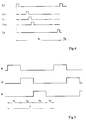
- FIG. 5 illustrates a preferred variant of the first embodiment for controlling a microtip color screen anode according to the present invention.
- a frame duration T provision is made for periods of color sub-frames Tr, Tg, Tb during which each of the bands of a color, red, green, blue, is sequentially polarized.
- a dead time Td is provided corresponding to an abovementioned regeneration phase. During this time Td, none of the three sets of anode bands are polarized.
- the cathode-grid assemblies are polarized to produce an emission of electrons.
- the period T of FIG. 5 can be identical to the period T of FIG. 3, in which case the durations of each of the sub-frames Tr, Tg, Tb will be reduced.
- the duration Td is preferably less than the duration of each of the color subframe periods so as not to significantly affect the brightness of the screen, if the anode-cathode voltage is not increased.
- the grid lines are preferably scanned as indicated above, the cathode lines remaining polarized at a high emission potential.
- This scanning can be carried out in a conventional manner as indicated in FIG. 4, each grid being sequentially polarized at its high potential.
- An advantage of the first embodiment of the present invention is that the desired result is obtained without modifying the structural characteristics of a device for controlling a microtip screen. You just have to modify the programming of the lines, columns decoding circuits and groups of anode bands. It will also be noted that the scanning can be carried out very quickly and that the dead time can be brief compared to the duration of the color frames and subframes.
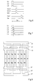
- FIG 8 illustrates a second embodiment of the present invention.
- the structure of the anode strips is changed so that each anode strip is divided into at least two addressable (polarizable) portions independently.
- Each anode strip is divided into two portions 9b-9b ', 9r-9r', 9g-9g '.
- the portions 9b, 9r and 9g are respectively connected to interconnection lines 12, 13 and 15.
- the portions 9b ', 9r' and 9g ' are respectively connected to interconnection lines 12', 13 'and 15'.
- the upper half (one color) of the anode is polarized and then we pass to the lower half to obtain the desired color subframe. While one half of the screen is addressed for display, a regeneration is carried out on the second half of the screen as described in relation to the first embodiment of the invention.
- An advantage of the second embodiment of the present invention is that the desired result is obtained without dead time at the cost of a simple structural modification.
- the invention also applies to luminescent screens whose anode potential is normally fixed. In such screens, it is also possible to provide a regeneration phase.
- the present invention is susceptible of various variants and modifications which will appear to those skilled in the art.
- the invention has been described in relation to a color screen to reduce the color drift, it also has the advantage of reducing anode-cathode or anode-grid breakdowns.
- it also applies to monochrome screens in which a dead time will be provided between displays of frames, for example after each frame.
- a monochrome screen in which the frame duration is 10 ms, the anode voltage of 250 to 300 V, and the brightness of 300 to 400 cd / m 2 , it is not possible to increase the anode voltage without having breakdowns.
- a regeneration step of, for example, 0.3 ms is provided at the end of each frame. The inventors have noted that the anode voltage could then be increased to 600 V without any breakdown occurring. As a result, the brightness has been increased to around 1000 cd / m 2 .
Landscapes
- Engineering & Computer Science (AREA)
- Physics & Mathematics (AREA)
- Computer Hardware Design (AREA)
- General Physics & Mathematics (AREA)
- Theoretical Computer Science (AREA)
- Control Of Indicators Other Than Cathode Ray Tubes (AREA)
Applications Claiming Priority (2)
| Application Number | Priority Date | Filing Date | Title |
|---|---|---|---|
| FR9507017 | 1995-06-08 | ||
| FR9507017A FR2735266B1 (fr) | 1995-06-08 | 1995-06-08 | Procede de commande d'ecran plat de visualisation |
Publications (2)
| Publication Number | Publication Date |
|---|---|
| EP0747875A1 true EP0747875A1 (de) | 1996-12-11 |
| EP0747875B1 EP0747875B1 (de) | 2006-10-04 |
Family
ID=9479937
Family Applications (1)
| Application Number | Title | Priority Date | Filing Date |
|---|---|---|---|
| EP96410067A Expired - Lifetime EP0747875B1 (de) | 1995-06-08 | 1996-06-04 | Steuerverfahren für eine flache Anzeigetafel |
Country Status (5)
| Country | Link |
|---|---|
| US (1) | US5872551A (de) |
| EP (1) | EP0747875B1 (de) |
| JP (1) | JP3985279B2 (de) |
| DE (1) | DE69636587T2 (de) |
| FR (1) | FR2735266B1 (de) |
Cited By (3)
| Publication number | Priority date | Publication date | Assignee | Title |
|---|---|---|---|---|
| FR2790861A1 (fr) * | 1999-01-29 | 2000-09-15 | Futaba Denshi Kogyo Kk | Dispositif d'attaque pour dispositif luminescent a emission par effet de champ |
| WO2001009870A1 (en) * | 1999-08-02 | 2001-02-08 | Motorola Inc. | Method for improving life of a field emission display |
| FR2804243A1 (fr) * | 2000-01-25 | 2001-07-27 | Pixtech Sa | Regeneration d'anodes d'ecran plat de visualisation |
Families Citing this family (2)
| Publication number | Priority date | Publication date | Assignee | Title |
|---|---|---|---|---|
| US6621475B1 (en) * | 1996-02-23 | 2003-09-16 | Canon Kabushiki Kaisha | Electron generating apparatus, image forming apparatus, method of manufacturing the same and method of adjusting characteristics thereof |
| FR2800510B1 (fr) | 1999-10-28 | 2001-11-23 | Commissariat Energie Atomique | Procede de commande de structure comportant une source d'electrons a effet de champ |
Citations (1)
| Publication number | Priority date | Publication date | Assignee | Title |
|---|---|---|---|---|
| DE4112078A1 (de) * | 1990-04-12 | 1991-10-17 | Futaba Denshi Kogyo Kk | Anzeigevorrichtung |
Family Cites Families (7)
| Publication number | Priority date | Publication date | Assignee | Title |
|---|---|---|---|---|
| JPS52123829A (en) * | 1976-04-12 | 1977-10-18 | Sony Corp | Color television receiver |
| US4366504A (en) * | 1977-10-07 | 1982-12-28 | Sharp Kabushiki Kaisha | Thin-film EL image display panel |
| JPS57162692U (de) * | 1981-04-03 | 1982-10-13 | ||
| FR2623013A1 (fr) * | 1987-11-06 | 1989-05-12 | Commissariat Energie Atomique | Source d'electrons a cathodes emissives a micropointes et dispositif de visualisation par cathodoluminescence excitee par emission de champ,utilisant cette source |
| US5172108A (en) * | 1988-02-15 | 1992-12-15 | Nec Corporation | Multilevel image display method and system |
| US5229691A (en) * | 1991-02-25 | 1993-07-20 | Panocorp Display Systems | Electronic fluorescent display |
| US5532712A (en) * | 1993-04-13 | 1996-07-02 | Kabushiki Kaisha Komatsu Seisakusho | Drive circuit for use with transmissive scattered liquid crystal display device |
-
1995
- 1995-06-08 FR FR9507017A patent/FR2735266B1/fr not_active Expired - Fee Related
-
1996
- 1996-06-04 DE DE69636587T patent/DE69636587T2/de not_active Expired - Lifetime
- 1996-06-04 EP EP96410067A patent/EP0747875B1/de not_active Expired - Lifetime
- 1996-06-06 US US08/660,710 patent/US5872551A/en not_active Expired - Lifetime
- 1996-06-07 JP JP16668396A patent/JP3985279B2/ja not_active Expired - Fee Related
Patent Citations (1)
| Publication number | Priority date | Publication date | Assignee | Title |
|---|---|---|---|---|
| DE4112078A1 (de) * | 1990-04-12 | 1991-10-17 | Futaba Denshi Kogyo Kk | Anzeigevorrichtung |
Cited By (4)
| Publication number | Priority date | Publication date | Assignee | Title |
|---|---|---|---|---|
| FR2790861A1 (fr) * | 1999-01-29 | 2000-09-15 | Futaba Denshi Kogyo Kk | Dispositif d'attaque pour dispositif luminescent a emission par effet de champ |
| WO2001009870A1 (en) * | 1999-08-02 | 2001-02-08 | Motorola Inc. | Method for improving life of a field emission display |
| FR2804243A1 (fr) * | 2000-01-25 | 2001-07-27 | Pixtech Sa | Regeneration d'anodes d'ecran plat de visualisation |
| EP1120772A1 (de) * | 2000-01-25 | 2001-08-01 | Pixtech S.A. | Regenerierung der Anoden einer flachen Anzeigetafel |
Also Published As
| Publication number | Publication date |
|---|---|
| FR2735266A1 (fr) | 1996-12-13 |
| FR2735266B1 (fr) | 1997-08-22 |
| EP0747875B1 (de) | 2006-10-04 |
| JP3985279B2 (ja) | 2007-10-03 |
| DE69636587D1 (de) | 2006-11-16 |
| US5872551A (en) | 1999-02-16 |
| DE69636587T2 (de) | 2007-07-05 |
| JPH0922270A (ja) | 1997-01-21 |
Similar Documents
| Publication | Publication Date | Title |
|---|---|---|
| EP0349425B1 (de) | Dreifarben-Leuchtschirm mit Mikrospitzen-Kathoden | |
| EP0356313B1 (de) | Verfahren zur sehr schnellen Ansteuerung einer wechselspannungsbetriebenen Plasmaanzeigetafel mit koplanarer Unterstützung durch halbselektive Adressierung und selektive Adressierung | |
| FR2709375A1 (fr) | Dispositif d'affichage d'images et circuit de commande associé. | |
| FR2721436A1 (fr) | Dispositif à affichage fluorescent et son procédé de commande. | |
| FR2787909A1 (fr) | Unite de chargement a plasma a nombre d'elements d'image pouvant etre excites de facon simultanee reduit de moitie | |
| EP0597772B1 (de) | Multiplexbetriebener Matrixbildschirm und Steuerverfahren dafür | |
| EP0349426B1 (de) | Mikrospitzen-Fluoreszenzbildschirm mit einer geringen Anzahl von Adressierungsschaltkreisen und Adressierungsverfahren von diesem Bildschirm | |
| EP0279746B1 (de) | Plasmapaneel mit vier Elektroden pro Elementarbildpunkt und Verfahren zur Steuerung eines solchen Plasmapaneeles | |
| EP0747875B1 (de) | Steuerverfahren für eine flache Anzeigetafel | |
| EP1814136B1 (de) | Ionenpumpen eines Flachbildschirms mit Mikropunkten | |
| EP0817232B1 (de) | Verfahren zur Regenerierung von Mikrospitzen einer flachen Anzeigetafel | |
| EP0734043B1 (de) | Doppel-Gate-Flaches Bildschirm | |
| FR2714209A1 (fr) | Dispositif d'affichage. | |
| EP0649162B1 (de) | Flaches Kaltkathodeanzeigegerät mit geschalteter Anode | |
| EP0337833A1 (de) | Punkt für Punkt Ansteuermethode für einen Plasma-Anzeiger | |
| EP0877407A1 (de) | Anode eines flachen Bildschirms | |
| EP1147538B1 (de) | Verfahren zur steuerung einer struktur mit einer elektronen-feldemissionsquelle | |
| FR2800512A1 (fr) | Ecran plat de visualisation a grille de protection | |
| EP0844642A1 (de) | Flaches Bildschirm mit fokussierenden Gittern | |
| EP1120772A1 (de) | Regenerierung der Anoden einer flachen Anzeigetafel | |
| FR2704967A1 (fr) | Ecran plat à micropointes à anode doublement commutée. | |
| FR2790861A1 (fr) | Dispositif d'attaque pour dispositif luminescent a emission par effet de champ | |
| FR2760283A1 (fr) | Procede et dispositif de reglage des coordonnees chromatiques d'un ecran plat de visualisation | |
| FR2798507A1 (fr) | Dispositif permettant de produire un champ electrique module au niveau d'une electrode et son application aux ecrans plats a emission de champ | |
| FR2654244A1 (fr) | Procede et dispositif d'adressage a grande vitesse pour l'entretien et l'adressage independants de panneaux d'affichage a plasma. |
Legal Events
| Date | Code | Title | Description |
|---|---|---|---|
| PUAI | Public reference made under article 153(3) epc to a published international application that has entered the european phase |
Free format text: ORIGINAL CODE: 0009012 |
|
| AK | Designated contracting states |
Kind code of ref document: A1 Designated state(s): DE FR GB IT |
|
| 17P | Request for examination filed |
Effective date: 19970521 |
|
| RAP1 | Party data changed (applicant data changed or rights of an application transferred) |
Owner name: COMMISSARIAT A L'ENERGIE ATOMIQUE |
|
| RAP1 | Party data changed (applicant data changed or rights of an application transferred) |
Owner name: PIXTECH S.A. |
|
| 111Z | Information provided on other rights and legal means of execution |
Free format text: DE FR GB IT |
|
| 17Q | First examination report despatched |
Effective date: 20011218 |
|
| 18D | Application deemed to be withdrawn |
Effective date: 20020429 |
|
| 19U | Interruption of proceedings before grant |
Effective date: 20020621 |
|
| D18D | Application deemed to be withdrawn (deleted) | ||
| 19W | Proceedings resumed before grant after interruption of proceedings |
Effective date: 20050502 |
|
| RAP1 | Party data changed (applicant data changed or rights of an application transferred) |
Owner name: LE COMMISSARIAT AE L'ENERGIE ATOMIQUE |
|
| GRAP | Despatch of communication of intention to grant a patent |
Free format text: ORIGINAL CODE: EPIDOSNIGR1 |
|
| GRAS | Grant fee paid |
Free format text: ORIGINAL CODE: EPIDOSNIGR3 |
|
| RAP1 | Party data changed (applicant data changed or rights of an application transferred) |
Owner name: COMMISSARIAT A L'ENERGIE ATOMIQUE |
|
| GRAA | (expected) grant |
Free format text: ORIGINAL CODE: 0009210 |
|
| AK | Designated contracting states |
Kind code of ref document: B1 Designated state(s): DE FR GB IT |
|
| PG25 | Lapsed in a contracting state [announced via postgrant information from national office to epo] |
Ref country code: IT Free format text: LAPSE BECAUSE OF FAILURE TO SUBMIT A TRANSLATION OF THE DESCRIPTION OR TO PAY THE FEE WITHIN THE PRESCRIBED TIME-LIMIT;WARNING: LAPSES OF ITALIAN PATENTS WITH EFFECTIVE DATE BEFORE 2007 MAY HAVE OCCURRED AT ANY TIME BEFORE 2007. THE CORRECT EFFECTIVE DATE MAY BE DIFFERENT FROM THE ONE RECORDED. Effective date: 20061004 |
|
| REF | Corresponds to: |
Ref document number: 69636587 Country of ref document: DE Date of ref document: 20061116 Kind code of ref document: P |
|
| GBT | Gb: translation of ep patent filed (gb section 77(6)(a)/1977) |
Effective date: 20061207 |
|
| PLBE | No opposition filed within time limit |
Free format text: ORIGINAL CODE: 0009261 |
|
| STAA | Information on the status of an ep patent application or granted ep patent |
Free format text: STATUS: NO OPPOSITION FILED WITHIN TIME LIMIT |
|
| 26N | No opposition filed |
Effective date: 20070705 |
|
| PGFP | Annual fee paid to national office [announced via postgrant information from national office to epo] |
Ref country code: DE Payment date: 20130611 Year of fee payment: 18 Ref country code: GB Payment date: 20130620 Year of fee payment: 18 |
|
| PGFP | Annual fee paid to national office [announced via postgrant information from national office to epo] |
Ref country code: IT Payment date: 20130618 Year of fee payment: 18 |
|
| PGFP | Annual fee paid to national office [announced via postgrant information from national office to epo] |
Ref country code: FR Payment date: 20130726 Year of fee payment: 18 |
|
| REG | Reference to a national code |
Ref country code: DE Ref legal event code: R119 Ref document number: 69636587 Country of ref document: DE |
|
| GBPC | Gb: european patent ceased through non-payment of renewal fee |
Effective date: 20140604 |
|
| REG | Reference to a national code |
Ref country code: DE Ref legal event code: R119 Ref document number: 69636587 Country of ref document: DE Effective date: 20150101 |
|
| REG | Reference to a national code |
Ref country code: FR Ref legal event code: ST Effective date: 20150227 |
|
| PG25 | Lapsed in a contracting state [announced via postgrant information from national office to epo] |
Ref country code: DE Free format text: LAPSE BECAUSE OF NON-PAYMENT OF DUE FEES Effective date: 20150101 Ref country code: IT Free format text: LAPSE BECAUSE OF NON-PAYMENT OF DUE FEES Effective date: 20140604 |
|
| PG25 | Lapsed in a contracting state [announced via postgrant information from national office to epo] |
Ref country code: GB Free format text: LAPSE BECAUSE OF NON-PAYMENT OF DUE FEES Effective date: 20140604 Ref country code: FR Free format text: LAPSE BECAUSE OF NON-PAYMENT OF DUE FEES Effective date: 20140630 |