EP0748056A2 - Fehlerdetektion und Korrekturverfahren für kodierten Datenstrom - Google Patents
Fehlerdetektion und Korrekturverfahren für kodierten Datenstrom Download PDFInfo
- Publication number
- EP0748056A2 EP0748056A2 EP96304168A EP96304168A EP0748056A2 EP 0748056 A2 EP0748056 A2 EP 0748056A2 EP 96304168 A EP96304168 A EP 96304168A EP 96304168 A EP96304168 A EP 96304168A EP 0748056 A2 EP0748056 A2 EP 0748056A2
- Authority
- EP
- European Patent Office
- Prior art keywords
- data
- traceback
- state
- path
- puncture
- Prior art date
- Legal status (The legal status is an assumption and is not a legal conclusion. Google has not performed a legal analysis and makes no representation as to the accuracy of the status listed.)
- Withdrawn
Links
- 238000012937 correction Methods 0.000 title claims description 8
- 238000001514 detection method Methods 0.000 title claims description 5
- 230000007704 transition Effects 0.000 claims abstract description 70
- 239000011159 matrix material Substances 0.000 claims abstract description 6
- 238000011084 recovery Methods 0.000 claims description 55
- 238000004364 calculation method Methods 0.000 claims description 24
- 238000000034 method Methods 0.000 claims description 23
- 230000005540 biological transmission Effects 0.000 claims description 10
- 238000012545 processing Methods 0.000 claims description 8
- 230000004044 response Effects 0.000 claims description 7
- 230000010363 phase shift Effects 0.000 claims description 6
- 230000003993 interaction Effects 0.000 claims description 3
- 238000005070 sampling Methods 0.000 claims description 3
- 238000004891 communication Methods 0.000 abstract description 5
- 238000010586 diagram Methods 0.000 description 30
- 238000004422 calculation algorithm Methods 0.000 description 11
- 238000013139 quantization Methods 0.000 description 10
- 230000008569 process Effects 0.000 description 9
- 238000012360 testing method Methods 0.000 description 7
- 230000003111 delayed effect Effects 0.000 description 6
- 238000013461 design Methods 0.000 description 6
- 230000006870 function Effects 0.000 description 6
- 230000003044 adaptive effect Effects 0.000 description 5
- 230000006872 improvement Effects 0.000 description 5
- 238000004088 simulation Methods 0.000 description 5
- 230000000694 effects Effects 0.000 description 3
- 230000008520 organization Effects 0.000 description 3
- 238000010079 rubber tapping Methods 0.000 description 3
- 230000001360 synchronised effect Effects 0.000 description 3
- HTRJZMPLPYYXIN-UHFFFAOYSA-N 2-acetamido-3-[[4-[(2-acetamido-2-carboxyethyl)sulfanylcarbothioylamino]phenyl]carbamothioylsulfanyl]propanoic acid Chemical compound CC(=O)NC(C(O)=O)CSC(=S)NC1=CC=C(NC(=S)SCC(NC(C)=O)C(O)=O)C=C1 HTRJZMPLPYYXIN-UHFFFAOYSA-N 0.000 description 2
- 230000008859 change Effects 0.000 description 2
- 230000000295 complement effect Effects 0.000 description 2
- 230000001186 cumulative effect Effects 0.000 description 2
- 238000001914 filtration Methods 0.000 description 2
- 238000005259 measurement Methods 0.000 description 2
- 238000012544 monitoring process Methods 0.000 description 2
- 230000000644 propagated effect Effects 0.000 description 2
- 230000003595 spectral effect Effects 0.000 description 2
- NCGICGYLBXGBGN-UHFFFAOYSA-N 3-morpholin-4-yl-1-oxa-3-azonia-2-azanidacyclopent-3-en-5-imine;hydrochloride Chemical group Cl.[N-]1OC(=N)C=[N+]1N1CCOCC1 NCGICGYLBXGBGN-UHFFFAOYSA-N 0.000 description 1
- 101100457838 Caenorhabditis elegans mod-1 gene Proteins 0.000 description 1
- 101150110972 ME1 gene Proteins 0.000 description 1
- 230000008901 benefit Effects 0.000 description 1
- 239000000872 buffer Substances 0.000 description 1
- 239000000969 carrier Substances 0.000 description 1
- 239000013078 crystal Substances 0.000 description 1
- 238000013016 damping Methods 0.000 description 1
- 238000013144 data compression Methods 0.000 description 1
- 230000003247 decreasing effect Effects 0.000 description 1
- 230000001419 dependent effect Effects 0.000 description 1
- 238000005516 engineering process Methods 0.000 description 1
- 238000012986 modification Methods 0.000 description 1
- 230000004048 modification Effects 0.000 description 1
- 230000036961 partial effect Effects 0.000 description 1
- 230000001902 propagating effect Effects 0.000 description 1
- 230000002829 reductive effect Effects 0.000 description 1
- 230000000717 retained effect Effects 0.000 description 1
- 229920006395 saturated elastomer Polymers 0.000 description 1
- 238000001228 spectrum Methods 0.000 description 1
- 230000003068 static effect Effects 0.000 description 1
- 238000004148 unit process Methods 0.000 description 1
Images






















Classifications
-
- H—ELECTRICITY
- H03—ELECTRONIC CIRCUITRY
- H03M—CODING; DECODING; CODE CONVERSION IN GENERAL
- H03M13/00—Coding, decoding or code conversion, for error detection or error correction; Coding theory basic assumptions; Coding bounds; Error probability evaluation methods; Channel models; Simulation or testing of codes
-
- H—ELECTRICITY
- H04—ELECTRIC COMMUNICATION TECHNIQUE
- H04L—TRANSMISSION OF DIGITAL INFORMATION, e.g. TELEGRAPHIC COMMUNICATION
- H04L1/00—Arrangements for detecting or preventing errors in the information received
- H04L1/004—Arrangements for detecting or preventing errors in the information received by using forward error control
- H04L1/0056—Systems characterized by the type of code used
- H04L1/0064—Concatenated codes
- H04L1/0065—Serial concatenated codes
-
- H—ELECTRICITY
- H03—ELECTRONIC CIRCUITRY
- H03M—CODING; DECODING; CODE CONVERSION IN GENERAL
- H03M13/00—Coding, decoding or code conversion, for error detection or error correction; Coding theory basic assumptions; Coding bounds; Error probability evaluation methods; Channel models; Simulation or testing of codes
- H03M13/03—Error detection or forward error correction by redundancy in data representation, i.e. code words containing more digits than the source words
- H03M13/23—Error detection or forward error correction by redundancy in data representation, i.e. code words containing more digits than the source words using convolutional codes, e.g. unit memory codes
-
- H—ELECTRICITY
- H03—ELECTRONIC CIRCUITRY
- H03M—CODING; DECODING; CODE CONVERSION IN GENERAL
- H03M13/00—Coding, decoding or code conversion, for error detection or error correction; Coding theory basic assumptions; Coding bounds; Error probability evaluation methods; Channel models; Simulation or testing of codes
- H03M13/37—Decoding methods or techniques, not specific to the particular type of coding provided for in groups H03M13/03 - H03M13/35
- H03M13/39—Sequence estimation, i.e. using statistical methods for the reconstruction of the original codes
- H03M13/41—Sequence estimation, i.e. using statistical methods for the reconstruction of the original codes using the Viterbi algorithm or Viterbi processors
-
- H—ELECTRICITY
- H03—ELECTRONIC CIRCUITRY
- H03M—CODING; DECODING; CODE CONVERSION IN GENERAL
- H03M13/00—Coding, decoding or code conversion, for error detection or error correction; Coding theory basic assumptions; Coding bounds; Error probability evaluation methods; Channel models; Simulation or testing of codes
- H03M13/37—Decoding methods or techniques, not specific to the particular type of coding provided for in groups H03M13/03 - H03M13/35
- H03M13/39—Sequence estimation, i.e. using statistical methods for the reconstruction of the original codes
- H03M13/41—Sequence estimation, i.e. using statistical methods for the reconstruction of the original codes using the Viterbi algorithm or Viterbi processors
- H03M13/4161—Sequence estimation, i.e. using statistical methods for the reconstruction of the original codes using the Viterbi algorithm or Viterbi processors implementing path management
- H03M13/4169—Sequence estimation, i.e. using statistical methods for the reconstruction of the original codes using the Viterbi algorithm or Viterbi processors implementing path management using traceback
-
- H—ELECTRICITY
- H03—ELECTRONIC CIRCUITRY
- H03M—CODING; DECODING; CODE CONVERSION IN GENERAL
- H03M13/00—Coding, decoding or code conversion, for error detection or error correction; Coding theory basic assumptions; Coding bounds; Error probability evaluation methods; Channel models; Simulation or testing of codes
- H03M13/63—Joint error correction and other techniques
- H03M13/635—Error control coding in combination with rate matching
- H03M13/6362—Error control coding in combination with rate matching by puncturing
-
- H—ELECTRICITY
- H03—ELECTRONIC CIRCUITRY
- H03M—CODING; DECODING; CODE CONVERSION IN GENERAL
- H03M13/00—Coding, decoding or code conversion, for error detection or error correction; Coding theory basic assumptions; Coding bounds; Error probability evaluation methods; Channel models; Simulation or testing of codes
- H03M13/65—Purpose and implementation aspects
- H03M13/6502—Reduction of hardware complexity or efficient processing
-
- H—ELECTRICITY
- H04—ELECTRIC COMMUNICATION TECHNIQUE
- H04L—TRANSMISSION OF DIGITAL INFORMATION, e.g. TELEGRAPHIC COMMUNICATION
- H04L1/00—Arrangements for detecting or preventing errors in the information received
- H04L1/0001—Systems modifying transmission characteristics according to link quality, e.g. power backoff
- H04L1/0009—Systems modifying transmission characteristics according to link quality, e.g. power backoff by adapting the channel coding
-
- H—ELECTRICITY
- H04—ELECTRIC COMMUNICATION TECHNIQUE
- H04L—TRANSMISSION OF DIGITAL INFORMATION, e.g. TELEGRAPHIC COMMUNICATION
- H04L1/00—Arrangements for detecting or preventing errors in the information received
- H04L1/004—Arrangements for detecting or preventing errors in the information received by using forward error control
- H04L1/0045—Arrangements at the receiver end
- H04L1/0054—Maximum-likelihood or sequential decoding, e.g. Viterbi, Fano, ZJ algorithms
-
- H—ELECTRICITY
- H04—ELECTRIC COMMUNICATION TECHNIQUE
- H04L—TRANSMISSION OF DIGITAL INFORMATION, e.g. TELEGRAPHIC COMMUNICATION
- H04L1/00—Arrangements for detecting or preventing errors in the information received
- H04L1/004—Arrangements for detecting or preventing errors in the information received by using forward error control
- H04L1/0056—Systems characterized by the type of code used
- H04L1/0067—Rate matching
- H04L1/0068—Rate matching by puncturing
-
- H—ELECTRICITY
- H04—ELECTRIC COMMUNICATION TECHNIQUE
- H04L—TRANSMISSION OF DIGITAL INFORMATION, e.g. TELEGRAPHIC COMMUNICATION
- H04L1/00—Arrangements for detecting or preventing errors in the information received
- H04L1/004—Arrangements for detecting or preventing errors in the information received by using forward error control
- H04L1/0056—Systems characterized by the type of code used
- H04L1/0071—Use of interleaving
Definitions
- This invention relates generally to processing signals received from a communications channel. More particularly this invention relates to an integrated signal processing system for receiving signals suitable for use in the transmission of video, "hi-fi" audio, images or other high bit rate signals.
- Encoded transmission of inherently analog signals is increasingly practiced today as a result of advances in signal processing techniques that have increased the bit rate achievable in a channel. At the same time new data compression techniques have tended to reduce the bandwidth required to acceptably represent analog information.
- the Art is presently striving to more efficiently transmit video and audio data in applications such as cable television using digital techniques.
- quadrature amplitude modulation is a relatively sophisticated technique favored by practitioners of digital communications. This method involves two separate symbol streams, each stream modulating one of two carriers in quadrature. QAM is particularly useful in applications having a low signal-to-noise ratio. Multilevel QAM formats are also used to achieve spectral efficiency in applications having high signal-to-noise ratios. For example, 64- and 256-QAM can achieve spectral efficiencies of 5 - 7 bits/sec-Hz in cable television networks.
- Quadrature Phase Shift Keying is a special case of the general Quadrature Amplitude Modulation (QAM) scheme, useful in applications having a low signal-to-noise ratio.
- QAM Quadrature Amplitude Modulation
- the ITU-T International Telecommunications Union
- DVB Digital Video Broadcasting
- 16-QAM and 64-QAM are used in the DVB standard for digital cable broadcasting.
- QPSK a signal constellation consisting of 4 symbols is transmitted, each having a different phase and a constant amplitude.
- the scheme is implemented as the sum of orthogonal components, represented by the equation.
- a m be j ⁇ m where ⁇ m can be any of ⁇ 0, ⁇ /2, ⁇ , 3 ⁇ /2 ⁇ . It is necessary to transmit both sidebands in order to preserve the quadrature information.
- a preferred embodiment of the invention provides a transmission receiving system for a quadrature phase shift keyed stream of data which is randomized, convolutionally interleaved and punctured at a puncture rate and aligned by a decoder in a puncture phase, wherein the data is in symbols and is transmitted at a symbol rate in a signal constellation.
- An error corrected data stream is output by the system.
- An embodiment of the present invention has an I, Q demodulator which accepts the data at the transmitted symbol rate, an analog-to-digital converter for converting an analog output of the I,Q demodulator, and a sinc interpolator receiving samples from the analog-to-digital converter.
- a timing recovery circuit has a first numerically controlled oscillator operative at periods T, a first loop filter which is coupled to the interpolator and the first numerically controlled oscillator, and has an output responsive to a difference between the periods T and the received symbol rate.
- the first numerically controlled oscillator is responsive to the first loop filter and generates a signal that is representative of the interpolation distance between succeeding samples.
- the interpolator interpolates the received samples according to the interpolation distance, and produces an output signal representative of the values of the interpolated samples.
- a matched Nyquist filter is coupled to the interpolator.
- a carrier recovery circuit for controlling the I,Q demodulator has a second numerically controlled oscillator.
- a digital derotation circuit is responsive to the second numerically controlled oscillator and accepts an in phase component and a quadrature component of sampled signals.
- a phase error estimation circuit is coupled to an output of the derotation circuit, and a second loop filter is coupled to an output of the phase error estimation circuit.
- the second numerically controlled oscillator is responsive to the second loop filter.
- There is a constellation rotation unit for rotating the signal constellation of the symbols, and an m-step inner decoder operative in a first mode and a second mode.
- the m-step inner decoder includes a branch metric calculation unit for outputting branch metrics for a selected puncture rate and a selected puncture phase, a plurality of add-compare-select blocks for outputting values of path metrics that are derived from the branch metrics, comparing the values and selecting a minimum value.
- a rescaling unit operates on the outputs of the add-compare-select blocks for rescaling the outputs according to the minimum value.
- a state transition module is operative in the first mode of operation for detecting illegal state transitions of the value of the path metrics selected by the add-compare select blocks.
- the state transition module outputs estimates of the puncture rate, the puncture phase and a rotation correction for the symbols, and controls the branch metric calculation unit for varying the selected puncture rate and the selected puncture phase according to the estimates of the puncture rate and the puncture phase.
- the state transition module controls the constellation rotation unit using the estimate of rotation correction.
- a synchronization search unit is enabled in the second mode of operation and is responsive to the state transition module for identifying synchronization information in the data stream.
- a traceback module is linked to the add-compare-select blocks, and has a succession of traceback columns, wherein each column represents all historical data of selected values of paths determined at a point in time by the add-compare-select blocks.
- the traceback columns each have a plurality of traceback elements each accepting m bits of traceback data, wherein the traceback elements are addressed by predecoded select lines according to the contents of at least one previous traceback column.
- a deinterleaver is coupled to the m-step inner decoder.
- An outer decoder receives deinterleaved data from the deinterleaver, and a derandomizer is coupled to the outer decoder.
- An output interface is coupled to the derandomizer for outputting the error corrected data stream.
- the state transition module controls the branch metric calculation unit for varying the selected puncture rate and the selected puncture phase when the detected illegal state transitions exceed a predetermined value
- the rescale unit operates on the add-compare-select outputs to rescale the outputs to non-negative numbers.
- the outputs are rescaled as a function of previous states thereof.
- an output of each traceback column is placed on a precharged line, and the branch metric calculation unit processes m symbols at a time.
- the synchronization search unit provides a signal to the first control unit indicative of a search result, wherein the first control unit resumes a state of the first mode of operation when the signal indicates a failed search result.
- the synchronization search unit also searches for inverted sync bytes.
- the timing recovery circuit and the carrier recovery circuit use a feedback technique to process data prior to filtering by the matched Nyquist filter, wherein the timing recovery and carrier recovery error signals are derived from circuits following the respective recovery circuits.
- the invention provides a decoder for symbols of received data encoded according to a convolutional encoding scheme.
- the data is punctuated according to a puncturing matrix, and has a plurality of state values which describe a sequence of state transitions from a first state to a succeeding state, wherein a path is defined by the sequence of state transitions.
- the decoder has a generation unit that accepts the received data for calculating metrics of the transitions thereof from the first state to the succeeding state, wherein the metrics correspond to a likelihood that a measured path follows a path produced by the transmitter of the data.
- a selector responsive to the generation unit selects a path corresponding to the path produced by the transmitter of the data stream.
- a traceback unit maintains historical information representative of sequential decision operations of the selector.
- a counter is provided for counting illegal state transitions of the path selected by the selector, and a control unit, responsive to the counter, determines a puncture rate, and adjusts a puncture phase and the carrier rotation phase of the received data.
- the generation unit includes a branch metric generator for precalculating branch metrics, wherein the branch metrics are a measure of probability values associated with all legal transitions of received data from the first state to the succeeding state, and also includes a path metric generator that receives the precalculated branch metrics from the branch metric generator.
- the path metric generator and the selector evaluate m succeeding transitions in a cycle of operation, and comprise a plurality of add-compare-select blocks.
- Each of the add-compare-select blocks transmits m symbols of data to the traceback unit in one clock cycle.
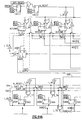
- Fig. 1 there is shown a block diagram of a portion of a receiver 2 embodying the teachings of the present invention. While the presently preferred embodiment is explained with reference to the European Telecommunication Standard prETS300421, the invention can be readily practiced in conjunction with other standards. Except for an I,Q demodulator 4 and its associated analog-to-digital converter, the receiver 2 is constructed according to a full CMOS design, and implemented as a single VLSI chip. Consequently its operation is far more efficient than that obtained with conventional board designs.
- the noted Telecommunication Standard provides inner convolutional encoding, and outer Reed-Solomon encoding of the transmitted data symbols.
- the receiver 2 provides an inner decoder and an outer decoder, as will be seen from the disclosure which follows.
- the receiver 2 accepts quadrature phase shift keyed data from a channel, for example, a satellite downlink.
- the data has been filtered and coded in several defined stages according to the noted European telecommunication standard, including: randomization and sync byte inversion for synchronization; Reed-Solomon encoding; Forney Interleaving; and in the case of satellite transmission, convolution encoding.
- Several defined puncture matrices are authorized by the standard.
- the I and Q signals are square-root raised cosine-filtered, with a roll-off factor of 0.35.
- an encoded, quadrature demodulated, near-baseband signal is provided by an I,Q demodulator 4 as an in-phase data stream 6 and a quadrature data stream 8.
- Feed-back timing recovery is accomplished in timing recovery circuitry 10.
- the processed in-phase and quadrature data are communicated to a DC removal block 12 on lines 14 and 16 respectively.
- symbol timing recovery T/2 spaced samples are indicated by the assertion of a control signal on line 18.
- Feedback carrier recovery is accomplished in carrier recovery circuitry 20, wherein said carrier recovery circuit receives an error signal that is derived in a feedback loop from a point beyond the carrier recovery circuitry 20.
- In-phase and quadrature data signals from which DC bias has been removed are transmitted to the carrier recovery circuitry 20 on lines 22 and 24 respectively, according to control signal 26.
- the timing recovery circuitry 10 and the carrier recovery circuitry 20 can be those disclosed in copending U.S. application Ser. No. 08/480,976, and British application Ser. No. 9511551.5 of common assignee herewith, which are hereby incorporated by reference.
- the resulting in-phase and quadrature signals are propagated to a matched Nyquist filter 28 on lines 30 and 32 respectively, according to control signal 34, followed by decimation by two in block 36.
- Feedback to the timing recovery circuitry 10 and the carrier recovery circuitry 20 is provided on feedback lines 38, 40, 42, and 44.
- the receiver 2 includes an automatic gain control circuit 46, which accepts decimated in-phase and quadrature data on buses 48 and 50 respectively according to control signal 52, and provides an output to the receiver front end (not shown) on line 54.
- the processed in-phase and quadrature data on buses 48, 50 are also provided to a Viterbi decoder 56.
- the current puncture rate of the received convolutionally encoded data is indicated on bus 58.
- Inversion of the received signal constellation is indicated by a signal on line 60.
- the I,Q demodulator 4 As the data processed through the I,Q demodulator 4 is Forney-interleaved, it is necessary to provide a deinterleaver 62, which accepts data on line 64. A valid control signal and an end-of-packet signal are provided to the deinterleaver 62 by the Viterbi decoder 56 on lines 66 and 68 respectively. The deinterleaved data stream is then passed to a Reed-Solomon decoder 70 on line 72. A valid control signal and an end-of-packet signal are provided to the Reed-Solomon decoder 70 on lines 74 and 76 respectively. The number of bit errors corrected in the current byte is indicated on bus 78.
- Decoded data is sent to a derandomizer and output interface 80 over line 82, using control signals on lines 84, 86, and 88.
- the control signals indicate whether a valid decoding has been accomplished, an end-of-packet status, and if there are errors in the data.
- Data is output on line 90.
- a signal on line 92 indicates when a sync byte is being output.
- Lines 94 and 96 indicate error condition and valid data respectively.
- a central control block 98 regulates the sequence of operation of other stages of the receiver 2.
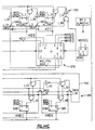
- the timing recovery circuitry 10 and the carrier recovery circuitry 20 are shown in greater detail in Fig. 2. These circuits are arranged such that the receiver 2 can work at many different symbol rates, or with variable symbol rate technology.
- a conventional off-chip I,Q baseband demodulator such as the GEC Plessey SL1710 I,Q demodulator is employed as the I,Q demodulator 4.
- An on-chip interpolator unit 89 under control of the timing recovery loop 100, generates synchronous T/2 spaced sample values. At each system clock tick, either one or zero T/2 samples are generated by the interpolator unit 89. In the event that a sample has been generated, subsequent hardware modules are so informed by the assertion of a "valid" control strobe 128 (Fig. 3).
- a fixed frequency external crystal oscillator 102 cooperates with an on-chip digital derotator 104, which operates at T/2 prior to the Nyquist filter 28, and an on-chip carrier recovery loop 106.
- the Nyquist filter 28 is preferably a finite-impulse-response (FIR) filter.
- the carrier recovery loop 106 operates with T/2-spaced samples.
- the I and Q outputs 108 and 110, respectively, are decimated by two in decimator block 36 (Fig. 1), and then applied to the error detection and correction circuits illustrated in the lower portion of Fig. 1.
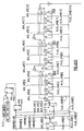
- the timing recovery circuit 10 (Fig. 1) is shown in greater detail in Figs. 3 and 4.
- Quadrature demodulated data is sampled at the system clock rate, which, as explained above, must be at least equal to the Nyquist frequency of the input data.
- an on-chip numerically controlled oscillator 112 keeps count of symbol time.
- the state ⁇ of the numerically controlled oscillator 112 represents a fixed point count of the number of symbol periods which have elapsed. At each system clock tick, the state ⁇ is incremented by a value in a register 114 equal to the (nominal baud rate ⁇ system clock rate), adjusted from the nominal using a control signal 116.
- a matched-filter derotator unit 129 includes the matched filters 124, 126.
- the matched filters 124, 126 are implemented as finite impulse response filters, and are enabled by a valid signal that is generated in the carrier recovery circuitry 20 (Fig. 1).
- the signals 137, and ⁇ 139 are accepted by a sinc interpolator unit 130, comprising an individual sinc interpolator 118, 115 for each of the in-phase and quadrature components.
- the interpolator unit 130 then generates a sample value based on the interpolation distance.
- ⁇ has a value greater than or equal to 0 and less than 1, but is represented as a fixed point number. Values greater than or equal to 1 are saturated to just less than 1.
- the sinc interpolator unit 130 is instructed to generate a leading or a lagging sample according to whether ⁇ is 1 or 0 respectively.
- the spread of sample times covered by the interpolator is one system clock period.
- the numerically controlled oscillator 112 operates in a timing loop based on the well known Gardner algorithm. Other timing recovery algorithms may also be used, such as the Müller and Müller algorithm.
- a section 132 contains a second order loop filter which is realized as a proportional-plus-integral controller 134. Its proportional and integral gain constants are selected to give the required damping factor and loop bandwidth. Preferably, a relatively wide bandwidth is used for initial channel acquisition in order to minimize lock time and insure acquisition. Thereafter the coefficients are changed to reduce the loop bandwidth and thereby make it less sensitive to noise and fluctuations. This "gear shifting" operation improves the overall system bit error rate.
- the matched filters 124, 126 are included because the Gardner algorithm assumes data having no intersymbol interference. They cannot be placed before the interpolator unit 130 because they have hard-wired coefficients designed for T/2 sampled data.
- the Gardner algorithm locks the timing sample point using T/2 samples.
- the loop preferably acquires the sample point such that odd samples are at the zero crossing points of the input data, and the even samples are used as data samples.
- the sinc interpolator unit 130 is based on a finite impulse response filter, which is clocked at the system clock rate, with the coefficients being selected from a bank of N sets, wherein each set of coefficients interpolates a different delay.
- the interpolation distance output from the numerically controlled oscillator 112 determines which bank of coefficients are used to generate a given sample, as ⁇ varies from 0 to 1.
- Sinc interpolation is based on the sampling theory which shows that a signal which has been Nyquist sampled can be reconstructed using sinc pulses, equivalent to performing a low pass filtering operation in the frequency domain. The output is given by the equation
- the timing recovery circuit 10 (Fig. 1) said timing recovery circuit receives an error signal that is derived in a feedback loop from a point beyond the timing recovery circuit.
- the DC removal block 12 (Fig. 1) is illustrated in further detail in Fig. 5, and comprises three modules 113, 117, and 122.
- Module 122 is used principally for testing the circuitry, and will not be further discussed. Only module 113 will be discussed, as the modules 113 and 117 are identical, and are applied to the I and Q data streams respectively.
- the module 113 is illustrated in detail in Fig. 6.
- Input data arrives in a 7-bit bus 124, is retimed in a flip-flop 123, and presented to an addition unit, referenced generally at 128, on bus 125.
- a submodule 127 monitors a feedback data stream that arrives on a bus 133, and calculates the DC offset for the data stream, which is placed on a bus 136. The DC offset is then subtracted from the input data in the addition unit 128.
- the addition unit 128 is conventionally arranged, and timed to operate at 60 MHZ.
- the output of the addition unit 128 is outputted onto a 7-bit bus 138.
- the structure of the submodule 127 is shown in Fig. 7. It principally comprises a 24-bit addition unit 140, which has a carry save architecture. Its input signal is on the bus 133, and is derived from the final output of the module 113 (Fig. 5). Timing considerations require the carry save architecture as the full addition cannot be evaluated in a single data cycle. Each carry output is retimed in a flip-flop 142 before being passed on to the next adder. To fully complete the addition, it is necessary to resolve all 24 carries, i.e. allow them to propagate. This is accomplished in the circuitry generally referenced 144, in three identical circuits 146, and in a row of adders 155.
- the final addition unit 154 is retimed due to time constraints, as it operates at 60MHz.
- a three stage adder block 156 Within the addition unit 154 is a three stage adder block 156, the structure of which is shown in Fig. 8. This is a fast adder wherein the carry status is rapidly selected in a combinatorial logical network 158, instead of allowing it to ripple through the three addition stages 160, 162, 164.
- the carrier recovery loop is explained initially with reference to Figs. 9 and 10, which illustrate a Costas algorithm phase error estimation section 166, a second order loop filter 168, a numerically controlled oscillator 170, and a digital derotation circuit 172.
- This circuit tracks any frequency errors and phase drift in the external modulation and demodulation chains.
- An additional adaptive loop circuit 174 (Fig. 10) can be used, operating according to the least-mean-square (LMS) algorithm to adaptively estimate demodulation phase noise errors caused by hum and jitter.
- LMS least-mean-square
- the adaptive loop circuit 174 is not included in the preferred embodiment.
- Sin ⁇ and cos ⁇ which are generated by use of a look-up table stored in a ROM (not shown), control the de-rotation circuit 172.
- ROM read-only memory
- the design of trigonometric look-up tables is well known.
- the calculation of I' and Q' is implemented in the network of multipliers and adders shown in the derotation circuit 172.
- the Costas phase error estimation section 166 completes the loop.
- the derotator 172 in cooperation with the phase estimation section 166, is also used to correct phase noise and jitter. This jitter is tracked by an LMS adaptive estimate of the phase error.
- the derotated I and Q values represented as fixed point numbers with a fractional part are sliced in slicers 176, 178 respectively to the nearest legal constellation value. For QPSK this will be +1 or -1.
- the difference between the derotated value and the sliced value is obtained in subtracters 180, 182, and forms the error.
- the I and Q error values are converted into an angular error estimate 8 error. In the case of QPSK modulation, the 8 error is obtained from a switching network contained in angulator 184, according to table 1 below.
- the output of the angulator 184 is an adapted LMS estimate of the phase jitter or hum error ⁇ estimate.
- the phase error estimation circuit disclosed in copending applications, U.S. Ser. No. 08/481,107, and British Application No. 9511568.9 of common assignee herewith, and incorporated herein by reference, can also be used, as may many other phase error estimation circuits, for example a circuit embodying the Costas algorithm.
- the adaptive algorithm has been modified slightly from the standard LMS algorithm in that the ⁇ estimate has been given a leak. Normally leak is zero, but every Nth cycle it is -(sign( ⁇ estimate)). This prevents the ⁇ error from growing beyond operational limits.
- the Costas loop locks with the constellation points on the axis - i.e., (1, 0), (0, 1), (-1, 0), (0, -1).
- ⁇ error is either + or -
- the proportional and integral gain constants of proportional integral controller 186 in the second order loop 168 start off with wide bandwidth values to minimize acquisition time, and are shifted to a lower bandwidth loop set of values to optimize the system bit error rate once lock has been achieved.
- the values can be readily selected in accordance with the requirements of a particular application.
- the bandwidth values are swept by repeatedly adding a constant value on line 151 to the integral gain constant in an adder 153. Lock occurs as the sweep progresses.
- the automatic gain control (AGC) circuit 46 comprises an AGC error block 183, which determines the error between the I, Q input signals on buses 48, 50 and the expected mean value thereof.
- An error signal is produced on bus 190 and is received by an AGC control block 192.
- the AGC control block 192 calculates a control voltage which is output on bus 194. The control voltage is dependent on the error signal on bus 190, and is averaged over time.
- the control voltage is fed to the receiver's front end (not shown) on output line 198
- the inputs on buses 48, 50 are retimed in flip-flops 200 and 202 respectively, and are complemented, if necessary, using exclusive OR gates 204, 206 as part of the absolute value function.
- a row of adders 208 adds the absolute value of the I input and the absolute value of the Q input. In the event complementing occurred, 1 is added to the two least significant bits of the sum, using adder 210, and two adders 212, 214 which are found in a second row of adders 216. The addition of the 1 completes the absolute value function.
- the expected mean value of the signal, binary 01000000, is then added to the thus modified output of the row of adders 208, and the result is outputted on the bus 190.
- Fig. 18 illustrates the structure of the AGC control block 192.
- the error signal on bus 190 is added to a control voltage on a bus, using a 22-bit adder, which is referenced generally at 218.
- the addition proceeds in a first stage 220 for the 8 least significant bits, and in a second stage 222 for the 14 most significant bits.
- the individual adders 224 are fast adders, using carry-by-pass propagation. Overflow and underflow conditions are detected by a logical network 226.
- the final control voltage is then placed on the bus 194 and fed back to the 22-bit adder 218 as a new control voltage.
- the sigma-delta modulator 196 is conventional, and is retimed to run at 7.5 MHZ in the preferred embodiment.
- An AGC level signal 234 is developed using the inverted most significant bit of the control voltage on bus 194, represented by line 230, and the next 7 bits of the control voltage, indicated by a bus 232.
- Fig. 12 is a time plot of the AGC level signal 234, referenced by the solid line 163, and of the output of the sigma-delta modulator 196 (Fig. 11) on output line 198, which is a series of pulses 165.
- the rate 1/2 indicates that for every one bit input, the encoder generates two bits.
- the constraint length K is the maximum number of signals that can be used to generate an output.
- a particular state S t can be represented by two bits.
- state S t can assume the value 2 (binary 10), indicated by reference numeral 169.
- the bits of state S t are shifted by one position, and an incoming data bit occupies the rightmost (least significant bit) position.
- the state value 169 can legally transition to values 171 and 173 in state S t+1 .
- the convolutional encoder will produce values 175 and 177 respectively, indicated more generally as x t y t . All possible state transitions can be calculated for the encoder, i.e. given S t and data bit d t , the next state S t+1 , x t and y t can be evaluated.
- the path metric is a measurement of the likelihood that the state is on the original encoder state sequence at that time. The smaller the path metric, the more probable the state is, and vice versa.
- the branch metric is a measurement of the probability value attached to each branch depending on the input. The branch metric is taken as the Hamming weight, which is the number of differing bits between a received symbol xy rx and an expected symbol xy along every branch in each transition as shown in Fig. 13. Traceback is the method of going back through the trellis to find the initial state which produced the state with the smallest path metric.
- a 2-step decoding process is employed, corresponding to moving through the trellis two steps at a time. This doubles the time to calculate each step, and each traceback yields two bits, rather than one.
- the number of calculations required at each state has also doubled, as each state now has four possible paths to be calculated. Only one path is required to be maintained in memory for each state. That path, known as the surviving path, is the one having the smallest path metric and is thus the most likely path.
- Puncturing is authorized in the noted European telecommunications standard, which has the effect of producing a higher rate of data transmission, as the code is more efficient.
- the convolutional encoder (not shown) encodes data to produce symbols x t and y t , which are then punctuated according to the puncturing matrix x: 1 0 y: 1 1 to produce-x' t and y' t , which are then retimed to be transmitted as I,Q in quadrature phase shift keyed modulation.
- the omitted bits do not contribute to the branch metric calculation.
- branch metrics were calculated using the Hamming Weight. Significant improvements result if, instead of receiving either a 1 or 0, we receive a multiple bit representation of each x rx and y rx showing the relative likelihood of the signal being a 1 or 0. Thus, in a 16 level (4-bit) soft decoding, a 1 is represented by 15 (binary 1111).
- the branch metrics may be calculated as shown in table 3.
- the respective path metrics are calculated using these soft-calculated branch metrics, giving significant improvements in decoder performance.
- an 8 level (3-bit) soft decoding is used. Traceback is implemented using a systolic array, as explained below in detail. Table 3 expected xy rx branch calculation result 00 0
- Fig. 14 A partial representation of a 2-step transition trellis diagram for this situation is illustrated in Fig. 14.
- the Viterbi decoder 56 has a rotation adjustment block 179, which receives in-phase and quadrature data on lines 48, 50. Validity of the incoming data is indicated by the state of a signal on line 52.
- the demodulator can lock the signal constellation in any of 8 carrier rotation phases, taking into consideration that it is possible for the received signal spectrum to be inverted in the sense that an I,Q symbol is received as a Q,I symbol. However, this condition is dealt with as discussed below, rather than in the rotation adjustment block 179.
- the present rotation phase is placed on a bus 181.
- branch metrics are calculated at each operation cycle in branch metric generation block 186, which is controlled by phase and punctuation control block 188.
- the current puncture rate on bus 185 and current puncture phase on bus 187 are input to the phase and punctuation control block 188 from a higher control block, which is Viterbi control block 195.
- States in the branch metric generation block 186 are mapped and selected for puncturing and phase adjustment according to the state of lines 197, 199, 201, and 203.
- the phase and punctuation control block 188 is shown in greater detail in Fig. 17.
- the maximum number of phases is derived from the puncture rate on bus 185 by combinatorial logic network 205, and placed on bus 207.
- Phase counting is accomplished in section 209 by a three bit adder, referenced generally at 211, followed by a 4-bit subtracter, indicated at 213.
- the phase count, modulo the maximum number of phases is determined and submitted to phase calculation section 215, where the current puncture phase is added to the phase count in the same manner as in section 209.
- the current phase, modulo the maximum number of phases appears on bus 217.
- a global enable signal 219 is generated by a small logical network 221.
- the output of the phase calculation section 215 is also used in a block 223 to decode the phase and rate information on buses 187 and 217 to produce the signals on buses 197, 199, 201, and 203, which are communicated to the branch metric generation block 186 (Fig. 15).
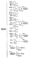
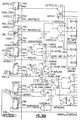
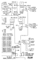
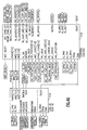
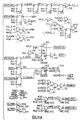
- the decode logic for buses 197 and 199 is shown in Figs. 19, 20, and 21, wherein individual bit positions are referenced on lines 225, 227, 228, 229, 231, 233 and 236.
- the signals on buses 201 and 203 (Fig.15) are complementary to those on buses 197 and 199 respectively.
- bus 199 selects a choice of I,Q inputs during branch generation
- bus 203 indicates where a puncture has occurred so that the data at the puncture location does not contribute to the path metric calculation.
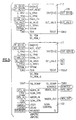
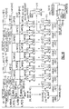
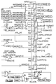
- the branch metric generation block 186 (Fig. 15) is shown in greater detail in Fig. 22. Pairs of I,Q data are received on lines 238, 240 respectively, and are processed in four combinatorial logic units 242, according to selector lines 225, 227, 228, 229, which are the complement of lines 197 (indicated as lines 244, 246, 248, 250), and the previous I,Q data on lines 252 and 254. From this data, two symbol XY pairs are reconstituted and presented to block 256 on lines 258, 260, 262, 264 for the generation of all 16 possible branch metrics on lines 266. The previous I,Q data is obtained from two delay flip-flops 268, 270.
- Block 256 is illustrated in greater detail in Fig. 23, and comprises 16 identical calculation units 272, one for each of the 16 possible branches.
- a representative calculation unit 272 is described in yet further detail in Fig. 24.
- Each calculation unit 272 includes four modules 274 in which the expected data is hard-wired.
- the modules 274 sum the absolute differences between the input data and the expected data for that particular branch, in the manner shown in Table 3, and force the data corresponding to punctuated positions to zero in accordance with the states of lines 201 and 203.
- the modules 274 comprise a simple logical network, which determines absolute differences, by inverting alternate bits.
- the four differences thus obtained on lines 278, 280, 282, 283 are summed in summing unit 284, which is illustrated in detail in Fig. 26, for output on lines 266 as the branch metric.
- path metrics are calculated in path metric generation block 189, utilizing the precalculated branch metrics obtained from the branch metric generation block 186 on lines 288. Precalculation of the branch metrics greatly simplifies the calculation of the path metrics.
- the path metric generation block 189 is able to process 2 symbols in one clock cycle.
- the branch metric generation block 186 and the path metric generation block 189 can optionally be generalized to process m symbols in a single clock cycle using an m-stage Viterbi decoder.
- the organization of the path metric generation block 189 is initially shown, by way of example, in Fig. 28, where the calculation of a path metric for state 0 is shown.
- a full expansion of the trellis diagram illustrated in Fig. 14 would show that at S t+1 , state 0 can legally receive transitions from states 0, 16, 32, and 48, referenced as 290, 292, 294 and 296 respectively. These transitions are referred to in Table 4 as paths 0 - 3 respectively, corresponding to the two most significant bits of their state number.
- Table 4 discloses the branch metrics for each legal transition in the transitional trellis diagram of Fig. 14.
- path 0 has expected branch data of 0; path 1 expects 14; path 2 expects 3; and path 3 expects 13.
- the branch metrics for each expected branch data are calculated.
- the previous path metric for state 0 is added to the branch metric with expected data 0, using adder 298 to give candidate 0 on line 300, and so on for the other three paths.
- the next path metric for state 0 is the smallest candidate value, and is output on line 304.
- the other candidates are discarded, as they are non-optimum paths.
- Two data bits passed onto the traceback indicate which path was chosen as having the smallest path metric, i.e. path 0, 1, 2 or 3, as required to trace back in time.
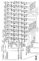
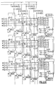
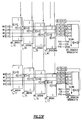
- the path metric generation block 189 comprises 64 add-compare-select blocks 306, one of which is fully shown in a fragmentary view in Fig. 29. Each of the add-compare-select blocks 306 generates a path metric. In actual layout, it is convenient to arrange the 64 add-compare-select blocks 306 in two groups of 32. This is a more compact design which minimizes the length and thus the driving requirements of the path metric routing crossbar. The smallest of the 64 path metrics is determined in the path metric generation block 189. Each of the add-compare-select blocks 306 receives four path metrics of a previous state each on 6-bit buses 308, 310, 312, 314, corresponding to transitions such as shown in Fig. 14. The corresponding branch metrics are received on 5-bit buses 316, 318, 320, and 322.
- Fig. 27 illustrates the arrangement of an add-compare-select block 306 in greater detail, wherein a minimum path metric of the 4 candidate path metrics input thereto is determined.
- the candidate path metrics are obtained in adders 324 by the addition of a path metric and a branch metric which are input on buses 326 and 328 respectively.
- the minimum path metric is then determined in compare module 330.
- Compare module 330 is shown in further detail in Fig. 30, in which four values are compared to find the minimum. In the six units 332 at the left side of Fig. 30, all possible comparisons are made and outputted on lines 334, 336.
- the outputs on lines 336 are simply the inversions of the outputs on lines 334 for each respective unit 332.
- the results are then decoded in a logical network 338 and placed on a four-bit select bus 340.
- a traceback unit 191 two bits of information are provided to a traceback unit 191 on lines 342 and 344 at each data cycle of operation of each add-compare-select block 306. Selection of the smallest path metric is accomplished using multiplexers referenced generally 346. To allow the path metric to be represented by six bits in order to reduce hardware, a rescaling unit 348 rescales the smallest path metric in an adder 350.
- the delay is employed because 2 cycles are required to calculate the smallest path metric.
- the rescaling function utilized guarantees that the rescaled value RV will never be negative.
- the rescaled path metric is output on bus 352.
- the Viterbi decoder 56 has a control block 195, which has several functions.
- a first mode of operation illegal state transitions of the path having the smallest path metric are counted as a measure of whether the currently estimated puncture rate, puncture phase and carrier phase have been correctly determined. Based on the illegal state transition count, a new combination of puncture rate, puncture phase, and carrier phase are chosen. If the illegal state transition count is within a specified tolerance, a second mode of operation is initiated, wherein an output data stream is enabled in which a correct synchronization pattern is sought. However, the end-state of the first mode of operation is retained. Hence if synchronization is not achieved, the first mode of operation is resumed at the end-state. This can be appreciated with reference to Fig. 31. Initially, in step 354, the illegal state counter and a wait counter are reset. At decision step 356 a check is immediately made to determine of a permissible number of illegal states transitions has been exceeded.
- step 370 A test is next made at step 370 for the occurrence of an illegal state transition. If an illegal state transition has not occurred, control immediately passes to decision step 360. If an illegal state transition has occurred, an illegal transition state counter is incremented at step 372. Otherwise control passes to step 358. Another test of the cumulative number of illegal state transitions is performed in decision step 374. If the number of illegal states is still within tolerance, control passes to step 358. Otherwise step 366 is executed, as will be explained below.
- step 358 The wait counter is incremented in step 358.
- decision step 360 a test is made to determine if the 256 cycles have been evaluated, according to the state of the wait counter. If not, control retums to step 356. If 256 cycles have been evaluated and the illegal state transitions remain within tolerance, synchronization search is activated in step 362. Control then proceeds to decision step 364, wherein activity of the synchronization unit is tested. Until synchronization fails, control remains in step 364.
- Step 366 is a decision step wherein a test is made for exhaustion of all possible combinations of puncture phases and carrier phases. If these have not been exhausted, the carrier phase is changed in step 368, and control returns to step 354. If the test at decision step 366 fails, then a further test-is made at decision step 376 to determine if all puncture rates have been evaluated. If exhaustion has not occurred, then the puncture rate and phase are changed at step 378. If all puncture rates and phases have been evaluated, then tolerance is increased at step 380, and control again returns to step 354.
- the wait counter is incremented in incrementer 382, and its value placed on a bus 384.
- the wait counter is tested in combinatorial logic 386.
- the number of illegal transitions tolerated is signaled on bus 388, and tested against the illegal state count on bus 390 in a comparator unit 392.
- a pulse is then generated on line 394, outputted on line 396, and fed back via a logical network 398 to a controller unit 400.
- the controller unit 400 outputs a new carrier phase, puncture rate, puncture phase, and new tolerance limit on lines generally referenced 402, according to the procedure discussed with reference to Fig. 31.
- Illegal state transitions are signaled on line 404 as decoded by a logical network 406 taking the previous state as input. Transitions on line 404 are counted in incrementer 408, and the new count value placed on a bus 410.
- the second mode of operation looking for sync bytes in the data stream, is initiated on line 412.
- This line is the output of a combinatorial logic network 414, which is governed by several control signals, namely the state of the tolerance test line 396, the status of the wait counter on line 416, and the current state of the decoder's second mode of operation, which is indicated on line 418.
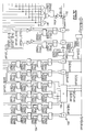
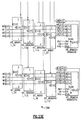
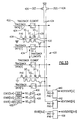
- the systolic traceback array unit 191 (Fig. 15) operates using a history of 21 periods in the preferred embodiment, and can be further understood with reference to Fig. 33.
- the traceback array unit 191 is linked to the add-compare-select blocks 306 (Fig. 29) of the path metric generation block 189, and includes a succession of traceback columns 420, each traceback column 420 representing all historical surviving paths determined at a point in time by the add-compare-select blocks 306 and the path metric generation block 189.
- Each traceback column 420 has a plurality of traceback elements 422, and each traceback element 422 accepts m bits of traceback data 424. As explained herein, m equals 2 in the currently preferred embodiment.
- the traceback column's traceback elements 424 are addressed by three predecoded select lines 426, 428, and 430 according to contents of at least one previous traceback column (not shown), as decoded by three decoders 432.
- the outputs of each traceback column 420 are placed on precharged lines 434.
- select lines 426, 428, and 430 are connected according to the state number of the previous traceback element, line 426 tapping the decoded state[1:0] corresponding to its state number, line 428 tapping State[3:2], and line 430 tapping State[5:4].
- the two precharge lines 434 are pulled to VDD.
- select lines 426, 428, and 430 are pulled down according to the traceback data.
- the state of the precharge lines 434 is latched in latches 440, 442 to be used for the 2 most significant bits for the next traceback column (not shown). It has been found that the use of precharged lines 434 greatly reduces the area required by the traceback unit 191.
- the method of quantifying these parameters is by simulation.
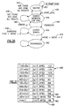
- the design of the simulation is shown in Fig. 34. Only simulations for rates 1/2 and 7/8 were performed as they represent the two extremes in encoding overhead.
- the curves are named as RrHhQq where r is code rate, h is history as a multiple of (K-1), where K is the constraint length, and q is the number of quantization levels used in soft decoding.
- the quantization figures are stated as the number of soft coding levels used.
- K is the constraint length.
- the synchronization strategy assumes a regularly spaced synchronization byte in the data stream. According to the noted European telecommunications standard, an inverted synchronization byte is transmitted in place of every 8th synchronization byte.
- the synchronization search unit 193 (Fig. 15) also assembles the two-bit output received from the traceback unit 191 on line 161 into bytes. This is accomplished by initially assembling 9-bits, and then evaluating two 8-bit bytes, each offset by one bit position. Both bytes thus assembled are evaluated, and a decision made for outputting one of them, according to which has a predefined synchronization bit pattern.
- Fig. 15 shows the synchronization search unit 193.
- the synchronization search unit 193 starts a search for valid sync bytes after receiving a start sync signal 159 from the control block 195.
- the search unit reports back to the control unit its state on the sync active line 157.
- the control unit enables the search unit after illegal state transitions are within tolerances.
- FIG. 35 A state diagram of the operation of the synchronization search unit 193 is depicted in Fig. 35.
- the search unit At the INACTIVE state 452 the search unit is in an inactive state as shown.
- signal IN_START_SYNC 444 is received from the control unit the search unit begins searching for a sync byte pattern of 47h or B8h in the SEARCH ANYWHERE state 446.
- the byte 47h corresponds to a positive sync pattern and B8h is an inverted sync pattern.
- the Viterbi decoder can operate on inverted data, a condition determined by noting the number of sync bytes, and the number of inverted sync bytes found by the synchronization search unit 193 (Fig. 15).
- the data that is being received from the traceback unit 191 (Fig. 15) is in 2-bit symbols. Because the decoder is utilizing a 2-step process, the start of a byte will be in one of two bit positions. The search unit therefore starts searching for the positive and negative sync byte pattern in two start bit positions. The search continues for every bit of a packet length of data as shown by the NOT FOUND AND NOT DONE ALL PACKET condition 448. If a full packet of data has been searched, and neither positive nor inverted sync has been found as shown by NOT FOUND DONE ALL PACKET condition 450, the search unit returns to the INACTIVE state 452 and signals the control unit 195 (Fig. 15) on sync active line 157 (Fig. 15) that the search was unsuccessful.
- the search unit When a sync pattern is detected, the search unit enters a LOCKED SEARCH state 454 following step FOUNDSYNC 456. In this state the search unit assumes that it has found a valid positive or inverted sync byte, and attempts to validate the sync by searching for the sync pattern in successive packet intervals where sync would be expected to be found. While in this state a count of successive valid and invalid sync bytes found is maintained. The search unit remains in this state until one of two conditions are met as indicated by loop SEARCHING SYNC + NSYNC ⁇ 8, referenced 458.
- the LOCKED SEARCH state 454 is exited and the search unit returns to the SEARCH ANYWHERE state 446 as shown by path ERROR > 3 460. Here it resumes the bit by bit search from the relative position in the packet where it previously was. If eight sync or inverted sync bytes are found to be valid, without incurring three or more errors, the search unit enters the SYNCHRONIZED state 462. Thereupon valid data is output. The search unit remains in this state until a channel change occurs.
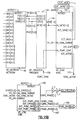
- Figs. 35 and 36 there is shown the logic diagram of the synchronization search unit.
- the combinational logic for decoding the sync byte patterns from the input data is realized by logic gates 464. These gates decode the positive and inverted sync byte patterns from the two bit start locations in the above noted 9-bit assembly.
- the SEARCH_COUNTER 466 is the counter associated with the SEARCH ANYWHERE state 446. During the LOCKED SEARCH state 454, the LOOK_COUNTER 468 is used.
- counter 470 When the search unit is in the LOCKED SEARCH state 454, counter 470 maintains a count of the inverted sync bytes found, counter 472 counts the positive sync bytes found, and counter 474 counts the erroneous sync bytes.
- the IN_START_SYNC signal from the control unit 195 (Fig. 15) is shown on line 476.
- the sync active signal to the control unit is shown as OUT_ACTIVE 478.
- the deinterleaver 62 will be discussed with reference to Figs. 1, 37 and 38. Twelveway Forney deinterleaving of transmitted data is specified in the above noted European Telecommunications standard. According to the interleaving process, a first byte flows through the interleaver without delay. A second byte is delayed by 17 cycles; a third byte is delayed by 2 x 17 cycles, etc. In the deinterleaver, the first byte is delayed by 11 x 17 cycles; a second byte is delayed by 10 x 17 cycles; a third byte is delayed by 9 x 17 cycles, etc. In the preferred embodiment 11 separate shift registers for deinterleaving the data have been implemented as a single block of 3-cycle synchronous static random access memory (RAM) 480. Pointers to base addresses within the memory 480, such as representative base addresses 482 and 484, are generated by a circuit 486.
- RAM 3-cycle synchronous static random access memory
- the first 11 x 17 bytes are used to implement an 11 x 17 byte shift register 488.
- a subsequent block of the memory 480 is allocated to a 10 x 17 byte shift register 490, and so on.
- the memory 480 is logically divided into 11 different sections, monotonically decreasing in size.
- Fig. 38-an adder 492 outputs an effective address for accessing the memory 480.
- a first input 494 of the adder 492 is a base address of the current shift register, i.e. 482.
- a second input 496 is the output of a byte counter 498, represented modulo 17.
- the third input 500 is the shifted-out value of an 11 x 4 bit shift register 502 multiplied by 17, which is a packet index into the current shift register, modulo length of the current shift register.
- the organization of the deinterleaver 62 (Fig. 1 ) can be appreciated with reference to Fig. 39, wherein the memory 480 has 1122 bytes. Operation of the memory 480 is controlled by a timing block 504, which initiates a memory read-write cycle, and increments the address counter 506.
- the memory 480 is attached to a write data bus 508, and a read data bus 510.
- Control signals include a valid signal on line 512, which is propagated from previous stages, and a read data valid signal on line 514, which indicates whether a memory read operation was successful.
- Block 516 is a control decode block for the I 2 C bus (not shown), used for writing to and reading from registers within the principal control block 518.
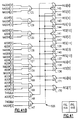
- the block 516 is discussed with reference to Fig. 41, which shows a serial data bus, and includes a first shift register 520 for decoding data, and a second shift register 522 for decoding addresses according to control signals.
- the output of the shift register 522 is placed on an 8-bit bus 524.
- the top 4 bits are used to decode the block currently being considered using logical network 526.
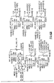
- Fig. 42 illustrates all the registers used in the central control block 98.
- Registers 528, 530, 532, 534, 536, 538, and 540 are written by the I 2 C bus to configure the central control block 98 (Fig. 1).
- a column of registers, generally referenced 542 are employed for monitoring the internal status of the central control block 98, and for monitoring retimed input signals on lines generally referenced 544, line 546, and line 548. It is possible for the I 2 C bus to read the central control block 98, as it is intended to be used with an external control device, such as a microprocessor, to interrogate and control the central control block 98.
- the central control block 98 contains circuitry compatible with the digital satellite equipment control standard DiSEqC (trademark).
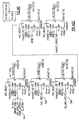
- FIG. 43 Further details of the central control block 98 are illustrated in Fig. 43.
- Several clock buffers are generally referenced 550. Retiming of inputs from other parts of the receiver 2 (Fig. 1) occurs in five flip-flops 552.
- Two multiplexers 554, 556 select outputs to the timing recovery circuitry 10, and the carrier recovery circuitry 20 (Fig. 1) on buses 558 and 560 respectively, according to the state of the channel lock state machine 562.
- the reciprocal of the value on bus 564 is calculated in block 566, which corresponds to the reciprocal generator 118 (Fig. 4), and is used for timing recovery.
- Consecutive and cumulative packet errors detected in the Reed-Solomon decoder 70 (Fig. 1) are counted in block 568.
- Another counter block 570 counts the decoder symbols immediately prior to processing by the Viterbi decoder 56, accepting an input on line 52 (Fig. 1). It produces control signals on lines 572, 574, and 576 for indicating that channel lock state machine 562 is to transition to its next state.
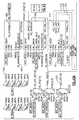
- a row of fast adders 578 repeatedly subtracts the data input, taken from a bus 580, from the value held in the shift register 582. If this operation does not result in an overflow, the result is selected in a plurality of multiplexers 584. If an overflow occurs, however, the original value in the shift register 586 is selected. the data is then shifted toward the most significant bit position of the shift register 580 at the left side of Fig. 44, and the subtract operation is repeated.
- a second shift register 586 is initialized to zero, except for the register 588 in the least significant bit position.
- the shift register 586 receives the final carry output from the row of adders 578 on line 590.
- the shift register 586 contains one extra register 592.
- the bit originally set in register 588 arrives in the register 594.
- the preceding register 591 is then tested for the presence of an overflow bit. If an overflow bit is present in register 591, a saturation signal is asserted on line 595, and the contents of the shift register 586 are all set to one.
- the original bit set in register 588 arrives in the register 592.
- the shift register 582 is then disabled according to control lines 596, 599.
- the reciprocal is output from the shift register 586 onto a bus 598.
- the channel lock state machine 562 (Fig. 43) is partly controlled by the input and symbol count of block 570.
- the block 562 drives the channel change control signals to various parts of the receiver 2 (Fig. 1), and also signals interrupts according to various failures on interrupt lines 600.
- Block 562 also controls the multiplexers 554, 556.
- the block 602 provides a bit error rate indication, and incorporates an infinite impulse response filter, shown in Fig. 45.
- a flip-flop 604 retimes the main interrupt line 606 for the receiver, according to chip event control line 608, and the setting of an interrupt mask on line 610.
- Block 602 which monitors the output from the Reed-Solomon decoder 70 (Fig. 1), is illustrated in further detail in Fig. 45.
- the detected bit error count for each byte is received on a bus 612.
- a group of subtracters 614 subtract a fractional portion, 1/2 13 , of the bit error rate every 64 symbols, which is approximately equivalent to subtracting 1/2 19 of the bit error rate once every symbol. This arrangement reduces the area required for the module, as the number of adders can be substantially reduced.
- BER scaled bit error rate
Landscapes
- Engineering & Computer Science (AREA)
- Physics & Mathematics (AREA)
- Probability & Statistics with Applications (AREA)
- Theoretical Computer Science (AREA)
- Computer Networks & Wireless Communication (AREA)
- Signal Processing (AREA)
- Artificial Intelligence (AREA)
- Quality & Reliability (AREA)
- Error Detection And Correction (AREA)
- Digital Transmission Methods That Use Modulated Carrier Waves (AREA)
- Detection And Correction Of Errors (AREA)
- Signal Processing For Digital Recording And Reproducing (AREA)
Applications Claiming Priority (4)
| Application Number | Priority Date | Filing Date | Title |
|---|---|---|---|
| US08/480,976 US5724396A (en) | 1995-06-07 | 1995-06-07 | Signal processing system |
| GB9605190A GB2302779A (en) | 1995-06-07 | 1996-03-12 | Decoding punctured convolutionally encoded data |
| GB9605190 | 1996-03-12 | ||
| US480976 | 2000-01-11 |
Publications (2)
| Publication Number | Publication Date |
|---|---|
| EP0748056A2 true EP0748056A2 (de) | 1996-12-11 |
| EP0748056A3 EP0748056A3 (de) | 1997-07-02 |
Family
ID=26308915
Family Applications (1)
| Application Number | Title | Priority Date | Filing Date |
|---|---|---|---|
| EP96304168A Withdrawn EP0748056A3 (de) | 1995-06-07 | 1996-06-06 | Fehlerdetektion und Korrekturverfahren für kodierten Datenstrom |
Country Status (6)
| Country | Link |
|---|---|
| EP (1) | EP0748056A3 (de) |
| JP (1) | JP3359817B2 (de) |
| KR (1) | KR100265674B1 (de) |
| CN (1) | CN1143288A (de) |
| AU (1) | AU699565B2 (de) |
| CA (1) | CA2178448A1 (de) |
Cited By (4)
| Publication number | Priority date | Publication date | Assignee | Title |
|---|---|---|---|---|
| WO2000069136A1 (fr) * | 1999-05-10 | 2000-11-16 | Anritsu Corporation | Dispositif numerique de mesure du signal de modulation et procede a cet effet capable d'evaluer le spectre de la composante de bruit |
| FR2817091A1 (fr) * | 2000-11-22 | 2002-05-24 | St Microelectronics Sa | Codeur a turbocodes a synchronisation facilitee |
| KR100437899B1 (ko) * | 1996-12-26 | 2004-11-03 | 엘지전자 주식회사 | 디지털무선채널시뮬레이터 |
| CN112114874A (zh) * | 2020-08-20 | 2020-12-22 | 北京百度网讯科技有限公司 | 数据处理方法、装置、电子设备和存储介质 |
Families Citing this family (3)
| Publication number | Priority date | Publication date | Assignee | Title |
|---|---|---|---|---|
| KR100441510B1 (ko) * | 2002-02-01 | 2004-07-23 | 삼성전자주식회사 | 채널상태정보를 적용된 데이터 에러 정정장치 |
| EP3032416A1 (de) * | 2014-12-10 | 2016-06-15 | Gemalto SA | Verfahren zum Ausführen einer empfindlichen Berechnung mit mehreren Verschiedenen und unabhängigen Zweigen |
| KR102675841B1 (ko) * | 2016-05-17 | 2024-06-18 | 삼성전자주식회사 | 바이너리 벡터 기반의 테스트 장치 |
Family Cites Families (5)
| Publication number | Priority date | Publication date | Assignee | Title |
|---|---|---|---|---|
| NZ198844A (en) * | 1980-11-14 | 1984-05-31 | Plessey Overseas | Digital information transmission: two dimensional code |
| US4932029A (en) * | 1987-07-24 | 1990-06-05 | Ant Nachrichtentechnik Gmbh | Method and apparatus for correcting errors in convolutional code signals |
| US5416787A (en) * | 1991-07-30 | 1995-05-16 | Kabushiki Kaisha Toshiba | Method and apparatus for encoding and decoding convolutional codes |
| US5363408A (en) * | 1992-03-24 | 1994-11-08 | General Instrument Corporation | Mode selective quadrature amplitude modulation communication system |
| US5438590A (en) * | 1993-05-24 | 1995-08-01 | Comstream Corporation | Transmitting and receiving apparatus and method including punctured convolutional encoding and decoding |
-
1996
- 1996-06-05 KR KR1019960019952A patent/KR100265674B1/ko not_active Expired - Lifetime
- 1996-06-06 AU AU55829/96A patent/AU699565B2/en not_active Ceased
- 1996-06-06 EP EP96304168A patent/EP0748056A3/de not_active Withdrawn
- 1996-06-06 CA CA002178448A patent/CA2178448A1/en not_active Abandoned
- 1996-06-07 JP JP18265496A patent/JP3359817B2/ja not_active Expired - Lifetime
- 1996-06-07 CN CN96110403A patent/CN1143288A/zh active Pending
Cited By (6)
| Publication number | Priority date | Publication date | Assignee | Title |
|---|---|---|---|---|
| KR100437899B1 (ko) * | 1996-12-26 | 2004-11-03 | 엘지전자 주식회사 | 디지털무선채널시뮬레이터 |
| WO2000069136A1 (fr) * | 1999-05-10 | 2000-11-16 | Anritsu Corporation | Dispositif numerique de mesure du signal de modulation et procede a cet effet capable d'evaluer le spectre de la composante de bruit |
| US6754260B1 (en) | 1999-05-10 | 2004-06-22 | Anritsu Corporation | Digital modulation signal measuring device and method capable of evaluating spectrum of noise component |
| FR2817091A1 (fr) * | 2000-11-22 | 2002-05-24 | St Microelectronics Sa | Codeur a turbocodes a synchronisation facilitee |
| WO2002043251A1 (fr) * | 2000-11-22 | 2002-05-30 | Stmicroelectronics S.A. | Codeur a turbocodes a synchronisation facilitee |
| CN112114874A (zh) * | 2020-08-20 | 2020-12-22 | 北京百度网讯科技有限公司 | 数据处理方法、装置、电子设备和存储介质 |
Also Published As
| Publication number | Publication date |
|---|---|
| KR100265674B1 (ko) | 2000-09-15 |
| EP0748056A3 (de) | 1997-07-02 |
| KR970004374A (ko) | 1997-01-29 |
| CA2178448A1 (en) | 1996-12-08 |
| JPH09219652A (ja) | 1997-08-19 |
| JP3359817B2 (ja) | 2002-12-24 |
| AU5582996A (en) | 1996-12-19 |
| CN1143288A (zh) | 1997-02-19 |
| AU699565B2 (en) | 1998-12-10 |
Similar Documents
| Publication | Publication Date | Title |
|---|---|---|
| US5742622A (en) | Error detection and correction system for a stream of encoded data | |
| US5878085A (en) | Trellis coded modulation communications using pilot bits to resolve phase ambiguities | |
| US5724396A (en) | Signal processing system | |
| KR100247373B1 (ko) | 신호 송신 장치, 신호 수신 장치, 및 신호 송수신방법 | |
| US5974091A (en) | Composite trellis system and method | |
| US7865812B2 (en) | Apparatus and method for determining a detected punctured position in punctured convolutional codes | |
| MXPA98000366A (en) | Device for decoding video signals coded in different way | |
| EP0840460A2 (de) | Annäherungspfad für einen Viterbi-Dekoder | |
| US6324224B1 (en) | Apparatus and method for receiving data with bit insertion | |
| US5822340A (en) | Method for decoding data signals using fixed-length decision window | |
| KR20000068741A (ko) | 디지털 데이터 전송장치 및 방법, 디지털 데이터 복조장치 및 방법, 및 전송매체 | |
| AU699565B2 (en) | An error detection and correction system for a stream of encoded data | |
| JP2000165463A (ja) | 復調器 | |
| EP1195909A1 (de) | Demodulationsverfahren und apparat | |
| GB2302779A (en) | Decoding punctured convolutionally encoded data | |
| US6075822A (en) | Traceback device of a trellis decoder | |
| HK1009621A (en) | An error detection and correction system for a stream of encoded data | |
| JPS62190934A (ja) | デ−タ復調装置 | |
| WO2003023974A1 (en) | Method and apparatus for constellation decoder | |
| US7164734B2 (en) | Decision directed phase locked loops (DD-PLL) with excess processing power in digital communication systems | |
| US6947503B2 (en) | Method and circuit for synchronizing a receiver for a convolutionally coded reception signal | |
| EP1524772B1 (de) | Verfahren und System zur Phasenrückgewinnung und Dekodierung | |
| TW312072B (en) | An error detection and correction system for a stream of encoded data | |
| JP3347682B2 (ja) | 誤り訂正回路 | |
| KR20030087425A (ko) | 격자 코드 데이타의 생존 경로 역추적장치 및 역추적방법 |
Legal Events
| Date | Code | Title | Description |
|---|---|---|---|
| PUAI | Public reference made under article 153(3) epc to a published international application that has entered the european phase |
Free format text: ORIGINAL CODE: 0009012 |
|
| AK | Designated contracting states |
Kind code of ref document: A2 Designated state(s): AT BE CH DE DK ES FR GB IE IT LI NL PT SE |
|
| PUAL | Search report despatched |
Free format text: ORIGINAL CODE: 0009013 |
|
| AK | Designated contracting states |
Kind code of ref document: A3 Designated state(s): AT BE CH DE DK ES FR GB IE IT LI NL PT SE |
|
| 17P | Request for examination filed |
Effective date: 19970821 |
|
| 17Q | First examination report despatched |
Effective date: 19971009 |
|
| STAA | Information on the status of an ep patent application or granted ep patent |
Free format text: STATUS: THE APPLICATION IS DEEMED TO BE WITHDRAWN |
|
| 18D | Application deemed to be withdrawn |
Effective date: 19991019 |
|
| REG | Reference to a national code |
Ref country code: HK Ref legal event code: WD Ref document number: 1009621 Country of ref document: HK |