EP0749095A2 - Standardkarte mit eingelagerter Minichipkarte - Google Patents
Standardkarte mit eingelagerter Minichipkarte Download PDFInfo
- Publication number
- EP0749095A2 EP0749095A2 EP96109533A EP96109533A EP0749095A2 EP 0749095 A2 EP0749095 A2 EP 0749095A2 EP 96109533 A EP96109533 A EP 96109533A EP 96109533 A EP96109533 A EP 96109533A EP 0749095 A2 EP0749095 A2 EP 0749095A2
- Authority
- EP
- European Patent Office
- Prior art keywords
- card
- mini chip
- standard
- chip card
- slots
- Prior art date
- Legal status (The legal status is an assumption and is not a legal conclusion. Google has not performed a legal analysis and makes no representation as to the accuracy of the status listed.)
- Granted
Links
Images

Classifications
-
- B—PERFORMING OPERATIONS; TRANSPORTING
- B42—BOOKBINDING; ALBUMS; FILES; SPECIAL PRINTED MATTER
- B42D—BOOKS; BOOK COVERS; LOOSE LEAVES; PRINTED MATTER CHARACTERISED BY IDENTIFICATION OR SECURITY FEATURES; PRINTED MATTER OF SPECIAL FORMAT OR STYLE NOT OTHERWISE PROVIDED FOR; DEVICES FOR USE THEREWITH AND NOT OTHERWISE PROVIDED FOR; MOVABLE-STRIP WRITING OR READING APPARATUS
- B42D25/00—Information-bearing cards or sheet-like structures characterised by identification or security features; Manufacture thereof
-
- G—PHYSICS
- G06—COMPUTING OR CALCULATING; COUNTING
- G06K—GRAPHICAL DATA READING; PRESENTATION OF DATA; RECORD CARRIERS; HANDLING RECORD CARRIERS
- G06K19/00—Record carriers for use with machines and with at least a part designed to carry digital markings
- G06K19/06—Record carriers for use with machines and with at least a part designed to carry digital markings characterised by the kind of the digital marking, e.g. shape, nature, code
- G06K19/067—Record carriers with conductive marks, printed circuits or semiconductor circuit elements, e.g. credit or identity cards also with resonating or responding marks without active components
- G06K19/07—Record carriers with conductive marks, printed circuits or semiconductor circuit elements, e.g. credit or identity cards also with resonating or responding marks without active components with integrated circuit chips
- G06K19/077—Constructional details, e.g. mounting of circuits in the carrier
- G06K19/07737—Constructional details, e.g. mounting of circuits in the carrier the record carrier consisting of two or more mechanically separable parts
- G06K19/07739—Constructional details, e.g. mounting of circuits in the carrier the record carrier consisting of two or more mechanically separable parts comprising a first part capable of functioning as a record carrier on its own and a second part being only functional as a form factor changing part, e.g. SIM cards type ID 0001, removably attached to a regular smart card form factor
-
- B42D2033/46—
Definitions
- the invention relates to a standard card with an embedded mini chip card, which contains an electronic module and which is partially separated along its outline edge by slots from the card body of the standard card and is connected to the card body of the standard card along the remaining outline edge by connecting areas.
- the invention further relates to a method for producing such cards.
- Standard cards with embedded mini chip cards are already known from EP 0 453 737 A1, in which the slots which separate the contour edge of the mini chip card from the card body of the standard card are produced by punching and lie practically along the entire contour edge.
- the mini chip card only remains connected to the card body of the standard card via narrow webs.
- the webs are designed so that they are either easy to break out or easy to punch out.
- the embedded mini chip cards known from EP 0 453 737 A1 have a high degree of dimensional accuracy, but it has been shown that the outline edges of the mini chip cards have burrs along the punched slots. These stamped burrs can lead to scratches when the standard cards are stacked with embedded mini chip cards.
- manually breaking the mini chip card out of the standard card body can lead to damage to the electronic module due to the tough web material, but at least the quality of the outline edge in the area of the broken webs is impaired. Punching out the webs, on the other hand, requires a special tool that is usually not always available on site.
- the mini chip card has been separated from the standard card body, it cannot be reinserted into the standard card body and fixed there.
- the manufacturing process avoids manual breakage of the webs, but it also leads to a punching ridge along the entire edge of the mini chip card and thus to the above. Problem.
- the mini chip card can be easily removed from the standard card body, but an exact reinsertion of the mini chip card into the standard card body is not possible due to the lack of attachment points.
- connection areas to the standard card body as long as possible along the outline edge of the mini chip card and these connection areas without the distance to be largely or completely severed from map material and to provide the remaining areas of the outline with slits.
- the area with the slits is small compared to the connection area.
- the slots preferably lie in the corner regions of the outline edge of the mini chip card and are produced by punching.
- the advantages of the invention can be seen in particular in that, on the one hand, the long connection areas between the mini chip card and the standard card body ensure that the mini chip card is adequately held in the standard card body and, on the other hand, there are no undesirable tensions between the mini chip card and the standard card body because of the slots mentioned .
- the mini chip card can be easily and manually removed from the standard card without any aids, since the connection areas of the mini chip card are largely or completely severed.
- the detached mini chip card has a clean, dimensionally stable outline, which is largely free of punch burrs, and can also be reinserted into the card body due to the press fit. The insertion is made easier by the small slots.
- the standard card with an embedded mini chip card can be produced in one operation.
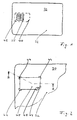
- FIG. 1 shows a standard card 30 with an electronic module 35 which lies in a recess in the card body 32.
- the dimensions of the card body 32 are specified in ISO standard 7810 and the position of the electronic module 35 in ISO standard 7816/2.
- the outline 40 of a mini chip card is indicated by the dash-dotted line, which, if it has certain dimensions, is also referred to as a plug-in card.
- the electronic module 35 lies in the mini chip card 42 and assumes a defined position in relation to the contour edge 40.
- FIG. 2 shows the partial area of the standard card 30, which has the mini chip card 42, on an enlarged scale and not to scale.
- the electronic module 35 is not shown in FIG. 2 because of the better overview and because it is of no importance for the following explanations.
- the outline edge 40 of the mini chip card 42 can be subdivided into a connection area, in which the mini chip card 43 remains connected to the standard card body 32, and into slots 44, which interrupt the connection area.
- connection areas are made as long as possible and largely or completely severed.
- the slots 44 also contain only a small proportion of the outline 40 compared to the connection areas.
- the connecting areas preferably take up almost the entire longitudinal and transverse sides of the outline edge 40 and merge into the slots 44 in at least one of the corner areas of the outline edge 40, as is also shown in FIG. 2.
- the connection areas end approx. 1 - 3 mm in front of the rounded corner areas.
- the slots 44 can also be located in other areas of the contour edge 40.
- the extensive or complete separation of the connection areas is preferably accomplished by cutting the card material of the standard card body 32, the cutting line lying exactly on the contour edge 40 of the mini chip card 42. During the cutting process, no material is removed from the card body 32, so that the cut outline edge 40 of the mini chip card 42 remains in contact with the card body 32 even after the cutting and the mini chip card 42 is held in a kind of press fit in the standard body 32.
- the slots 44 are preferably produced by punching, card material being removed from the standard card body 32, so that tensions between the mini chip card and the standard card body are avoided. It has been shown that extremely small slots are sufficient to avoid tension between the standard card body and the mini chip card.
- the incisions and the slots are created simultaneously, e.g. B. with a device as it is presented in the as yet unpublished patent application P 195 13 282.3, which is adapted accordingly.
- Fig. 3 shows a greatly enlarged and not to scale a cross section along the line AA of Fig. 2.
- the outline 40 is largely severed in the connection areas, which z. B. can be achieved by cutting the card material of the card body on both sides.
- the depth of cut of both incisions is preferably the same, so that a narrow core 20 remains in the middle of the contour edge 40.
- the core 20 has a thickness of approximately 150-450 ⁇ m, preferably 300 ⁇ m, so that the mini chip card 43 can be easily manually removed from the standard card body. Since the severed core lies in the center on the outline edge and can be made as thin as desired, the mini chip card that is separated out is therefore largely free of any punched burr in the connection area. It is also possible to completely sever the connection area mechanically during the production of the mini chip card 42. In this case, the mini chip card has no stamped burr at all in the connection areas after it has been removed from the standard card body.
- connection areas from the mini chip card 42 to the standard card body 32 are interrupted by the slots 44, one edge of the slots coinciding with the outline edge 40 of the mini chip card, as is shown in FIG. 3.
- the mini chip card 42 is not in contact with the standard card body 32, so that tensions within the mini chip card 42 are prevented and a reinsertion of the separated mini chip card into the standard card body 32 is facilitated. Since the slots 44 occupy only a small part of the contour edge 40, the punch burrs which are produced by punching out the slots on the contour edge 40 can be neglected.
Landscapes
- Engineering & Computer Science (AREA)
- Computer Hardware Design (AREA)
- Microelectronics & Electronic Packaging (AREA)
- Physics & Mathematics (AREA)
- General Physics & Mathematics (AREA)
- Theoretical Computer Science (AREA)
- Credit Cards Or The Like (AREA)
- Coupling Device And Connection With Printed Circuit (AREA)
Abstract
Description
- Die Erfindung betrifft eine Standardkarte mit eingelagerter Minichipkarte, die ein elektronisches Modul enthält und die entlang ihrer Umrißkante durch Schlitze bereichsweise von dem Kartenkörper der Standardkarte getrennt ist und entlang der verbleibenden Umrißkante durch Verbindungsbereiche mit dem Kartenkörper der Standardkarte verbunden ist. Die Erfindung betrifft ferner ein Verfahren zur Herstellung solcher Karten.
- Aus der EP 0 453 737 A1 sind bereits Standardkarten mit eingelagerten Minichipkarten bekannt, bei denen die Schlitze, die die Umrißkante der Minichipkarte von dem Kartenkörper der Standardkarte trennen, durch Stanzen erzeugt werden und praktisch entlang der gesamten Umrißkante liegen. Die Minichipkarte bleibt lediglich über schmale Stege mit dem Kartenkörper der Standardkarte verbunden. Hierbei sind die Stege so ausgebildet, daß sie entweder leicht ausbrechbar oder leicht ausstanzbar sind.
- Die aus der EP 0 453 737 A1 bekannten eingelagerten Minichipkarten weisen eine hohe Maßhaltigkeit auf, es hat sich jedoch gezeigt, daß die Umrißkanten der Minichipkarten entlang der gestanzten Schlitze Stanzgrate aufweisen. Diese Stanzgrate können bei einer Stapelung der Standardkarten mit eingelagerten Minichipkarten zu Kratzspuren führen. Darüber hinaus kann ein manuelles Herausbrechen der Minichipkarte aus dem Standardkartenkörper wegen des zähen Stegmaterials zu Beschädigungen des elektronischen Moduls führen, zumindest ist aber die Qualität der Umrißkante im Bereich der ausgebrochenen Stege beeinträchtigt. Ein Ausstanzen der Stege hingegen erfordert ein besonderes Werkzeug, das in der Regel vor Ort nicht immer vorhanden ist. Schließlich kann die Minichipkarte, nachdem sie einmal aus dem Standardkartenkörper getrennt wurde, nicht wieder in den Standardkartenkörper eingesetzt und dort fixiert werden.
- Aus den o.g. Gründen ist in der DE 41 32 270 A1 bereits vorgeschlagen worden, auf Stege, die die Minichipkarte mit dem Standardkartenkörper verbinden, ganz zu verzichten und die Minichipkarte mit Hilfe eines Klebefilmstreifens in dem Standardkartenkörper zu fixieren. Um eine exakte Position der Minichipkarte in dem Standardkartenkörper zu gewährleisten, wird die Minichipkarte aus dem Standardkartenkörper ausgestanzt, wobei sie zunächst noch über schmale Stege mit dem Standardkartenkörper verbunden bleibt. Danach wird der Klebefilmstreifen so aufgebracht, daß er die Minichipkarte mit dem Standardkartenkörper verbindet, anschließend werden die verbleibenden Stege ausgestanzt.
- Durch das Herstellungsverfahren wird ein manuelles Brechen der Stege vermieden, jedoch führt es ebenfalls zu einem Stanzgrat entlang der gesamten Umrißkante der Minichipkarte und damit zu dem o.g. Problem. Darüber hinaus kann die Minichipkarte zwar dem Standardkartenkörper einfach entnommen werden, jedoch ist ein exaktes Wiedereinsetzen der Minichipkarte in den Standardkartenkörper aufgrund fehlender Anschlagpunkte nicht möglich.
- Es ist deshalb Aufgabe der Erfindung, eine Standardkarte mit eingelagerter Minichipkarte vorzustellen, bei der die Minichipkarte ohne Hilfsmittel aus der Standardkarte herausgetrennt werden kann, nach dem Heraustrennen eine saubere Umrißkante aufweist und gegebenenfalls wieder in den Standardkartenkörper eingesetzt und in einer exakten Position fixiert werden kann. Es ist ferner Aufgabe der Erfindung, ein Herstellungsverfahren für eine solche Standardkarte mit eingelagerter Minichipkarte vorzustellen.
- Die Aufgabe wird bereits durch die noch nicht offengelegte Patentanmeldung mit dem Aktenzeichen P 195 13 282.3 der Anmelderin gelöst. Dort wird vorgeschlagen, die Umrißkante der Minichipkarte durch beidseitiges Einschneiden des Standardkartenkörpers zu erzeugen. Hierbei wird das Kartenmaterial ganz oder bis auf eine verbleibende extrem schmale "Seele" durchtrennt. Die ausgeschnittene Minichipkarte kann somit einerseits ohne Hilfsmittel aus dem Standardkartenkörper herausgetrennt werden. Andererseits löst sich die Minichipkarte nicht alleine aus dem Standardkartenkörper, da beim Einschneiden kein Kartenmaterial entfernt wird und die Minichipkarte deswegen in einer Art Preßpassung im Kartenkörper fixiert bleibt. Über diese Preßpassung läßt sich die herausgetrennte Minichipkarte auch wieder in einer exakten Position in den Standardkartenkörper einsetzen. Schließlich weist die geschnittene Umrißkante der Minichipkarte keine über die Oberfläche hinausragenden Stanzgrate auf.
- Es hat sich jedoch gezeigt, daß durch das Schneiden der gesamten Umrißkante zwischen der Minichipkarte und dem Standardkartenkörper Spannungen entstehen, so daß sich beide Karten wölben. Diese Spannungen kommen wohl durch das Eindringen der Schneidmesser in das Kartenmaterial und durch die Materialverdrängung in den Kartenkörpern zustande. Aufgrund der auftretenden Spannungen ist auch ein Wiedereinsetzen der Minichipkarte in den Standardkartenkörper relativ schwierig.
- Ausgehend von der Patentanmeldung mit dem Aktenzeichen P 195 13 282.3 verbleibt also die Aufgabe zu lösen, eine Verformung der Standardkarte mit eingelagerter Minichipkarte zu vermeiden und ein einfaches Wiedereinsetzen in den Standardkartenkörper zu ermöglichen.
- Die genannten Aufgaben werden durch die nebengeordneten Ansprüche 1 und 7 gelöst.
- Der Grundgedanke der Erfindung ist darin zu sehen, die Verbindungsbereiche zu dem Standardkartenkörper entlang der Umrißkante der Minichipkarte möglichst lang auszubilden und diese Verbindungsbereiche ohne die Entfernung von Kartenmaterial weitgehend oder vollständig zu durchtrennen und die übrigen Bereiche der Umrißkante mit Schlitzen zu versehen. Hierbei ist der Bereich mit den Schlitzen klein im Vergleich zu dem Verbindungsbereich. Vorzugsweise liegen die Schlitze in den Eckbereichen der Umrißkante der Minichipkarte und werden durch Stanzen erzeugt.
- Die Vorteile der Erfindung sind insbesondere darin zu sehen, daß einerseits durch die langen Verbindungsbereiche zwischen der Minichipkarte und dem Standardkartenkörper ein ausreichender Halt der Minichipkarte in dem Standardkartenkörepr gewährleistet ist und es andererseits wegen der genannten Schlitze nicht zu unerwünschten Spannungen zwischen der Minichipkarte und dem Standardkartenkörper kommt. Darüber hinaus kann die Minichipkarte einfach und ohne Hilfsmittel manuell aus der Standardkarte herausgetrennt werden, da die Verbindungsbereiche der Minichipkarte weitgehend oder vollständig durchtrennt sind. Die herausgetrennte Minichipkarte weist eine saubere maßhaltige Umrißkante auf, die weitgehend frei von Stanzgraten ist, und kann aufgrund der Preßpassung zum Kartenkörper auch wieder in diesen eingesetzt werden. Hierbei wird das Einsetzen durch die kleinen Schlitze erleichtert. Schließlich kann die Standardkarte mit eingelagerter Minichipkarte in einem Arbeitsgang hergestellt werden.
- Ausführungsbeispiele und weitere Vorteile der Erfindung werden im Zusammenhang mit den nachstehenden Figuren beschrieben. Darin zeigt:
- Fig. 1
- eine Standardkarte in Aufsicht,
- Fig. 2
- einen Ausschnitt aus einer Standardkarte mit eingelagerter Minichipkarte in Aufsicht,
- Fig. 3
- einen Querschnitt entlang der in der Fig. 2 gezeigten Linie A-A.
- Fig. 1 zeigt eine Standardkarte 30 mit einem elektronischen Modul 35, das in einer Aussparung des Kartenkörpers 32 liegt. Die Abmessungen des Kartenkörpers 32 sind in der ISO-Norm 7810 und die Position des elektronischen Moduls 35 ist in der ISO-Norm 7816/2 festgelegt. In der Fig. 1 ist durch die strichpunktierte Linie die Umrißkante 40 einer Minichipkarte angedeutet, die, wenn sie bestimmte Abmessungen aufweist, auch als Plug In-Karte bezeichnet wird. Das elektronische Modul 35 liegt in der Minichipkarte 42 und nimmt eine definierte Position zu der Umrißkante 40 ein.
- Fig. 2 zeigt vergrößert und nicht maßstabsgetreu den Teilbereich der Standardkarte 30,der die Minichipkarte 42 aufweist. Das elektronische Modul 35 ist wegen der besseren Übersicht und weil es für die nachfolgenden Ausführungen ohne Bedeutung ist, in der Fig. 2 nicht gezeigt. Die Umrißkante 40 der Minichipkarte 42 läßt sich in einen Verbindungsbereich, in dem die Minichipkarte 43 mit dem Standardkartenkörper 32 verbunden bleibt, und in Schlitze 44, die den Verbindungsbereich unterbrechen, unterteilen.
- Erfindungsgemäß werden die Verbindungsbereiche möglichst lang ausgebildet und weitgehend oder ganz durchtrennt. Erfindungsgemäß enthalten ferner die Schlitze 44 im Vergleich zu den Verbindungsbereichen nur einen geringen Anteil der Umrißkante 40.
- Vorzugsweise nehmen die Verbindungsbereiche nahezu die gesamten Längs- und Querseiten der Umrißkante 40 ein und gehen in mindestens einem der Eckbereiche der Umrißkante 40 in die Schlitze 44 über, wie es auch in der Fig. 2 gezeigt ist. Hierbei enden die Verbindungsbereiche jeweils ca. 1 - 3 mm vor den abgerundeten Eckbereichen. Selbstverständlich können die Schlitze 44 auch in anderen Bereichen der Umrißkante 40 liegen.
- Die weitgehende oder völlige Durchtrennung der Verbindungsbereiche wird vorzugsweise durch Einschneiden des Kartenmaterials des Standardkartenkörpers 32 herbeigeführt, wobei die Schnittlinie exakt auf der Umrißkante 40 der Minichipkarte 42 liegt. Bei dem Einschneiden wird kein Material aus dem Kartenkörper 32 entfernt, so daß die eingeschnittene Umrißkante 40 der Minichipkarte 42 auch nach dem Einschneiden in Kontakt mit dem Kartenkörper 32 steht und die Minichipkarte 42 in einer Art Preßpassung in dem Standardkörper 32 gehalten wird. Die Schlitze 44 werden hingegen vorzugsweise durch Stanzen erzeugt, wobei Kartenmaterial aus dem Standardkartenkörper 32 entfernt wird, so daß Spannungen zwischen der Minichipkarte und dem Standardkartenkörper vermieden werden. Hierbei hat es sich gezeigt, daß extrem kleine Schlitze ausreichen, um Spannungen zwischen dem Standardkartenkörper und der Minichipkarte zu vermeiden.
- Es ist besonders vorteilhaft, die Einschnitte in den Verbindungsbereichen und die Schlitze mit einem Werkzeug zu erstellen, da die Standardkarte 30 dann nur einmal in dem Werkzeug positioniert zu werden braucht und somit die Einschnitte entlang der Umrißkante der Minichipkarte und die Schlitzkanten, die auf der Umrißkante der Minichipkarte liegen, exakt ineinander übergehen. Vorzugsweise werden die Einschnitte und die Schlitze gleichzeitig erzeugt, z. B. mit einer Vorrichtung, wie sie in der noch nicht offengelegten Patentanmeldung P 195 13 282.3 vorgestellt wird, die entsprechend angepaßt ist.
- Fig. 3 zeigt stark vergrößert und nicht maßstabsgetreu einen Querschnitt entlang der Linie A-A der Fig. 2. Die Umrißkante 40 ist in den Verbindungsbereichen weitgehend durchgetrennt, was z. B. durch beidseitiges Einschneiden des Kartenmaterials des Kartenkörpers erreicht werden kann. Hierbei ist die Schnittiefe beider Einschnitte vorzugsweise gleich, so daß in der Mitte der Umrißkante 40 eine schmale Seele 20 verbleibt. Die Seele 20 weist eine Dicke von ca. 150 - 450 µm, vorzugsweise 300 µm, auf, so daß die Minichipkarte 43 manuell einfach aus dem Standardkartenkörper herausgetrennt werden kann. Da die durchtrennte Seele mittig auf der Umrißkante liegt und beliebig dünn ausgebildet werden kann, ist die herausgetrennte Minichipkarte also im Verbindungsbereich weitgehend frei von einem Stanzgrat. Es ist auch möglich, den Verbindungsbereich bei der Herstellung der Minichipkarte 42 maschinell ganz zu durchtrennen. In diesem Fall weist die Minichipkarte nach dem Heraustrennen aus dem Standardkartenkörper in den Verbindungsbereichen überhaupt keinen Stanzgrat auf.
- Die Verbindungsbereiche von der Minichipkarte 42 zum Standardkartenkörper 32 sind durch die Schlitze 44 unterbrochen, wobei eine Kante der Schlitze mit der Umrißkante 40 der Minichipkarte zusammenfällt, sowie es in der Fig. 3 gezeigt ist. Im Bereich der Schlitze 44 steht die Minichipkarte 42 nicht mit dem Standardkartenkörper 32 in Berührung, so daß Spannungen innerhalb der Minichipkarte 42 vorgebeugt ist und ein Wiedereinsetzen der herausgetrennten Minichipkarte in den Standardkartenkörper 32 erleichtert wird. Da die Schlitze 44 nur einen geringen Teil der Umrißkante 40 einnehmen, können die Stanzgrate, die durch Ausstanzen der Schlitze auf der Umrißkante 40 entstehen, vernachlässigt werden.
Claims (9)
- Standardkarte mit eingelagerter Minichipkarte, die ein elektronisches Modul enthält und die entlang ihrer Umrißkante durch Schlitze bereichsweise von dem Kartenkörper der Standardkarte getrennt ist und entlang der verbleibenden Umrißkante durch Verbindungsbereiche mit dem Kartenkörper der Standardkarte verbunden ist, dadurch gekennzeichnet, daß die Verbindungsbereiche entlang der Umrißkante der Minichipkarte weitgehend oder vollständig durchtrennt sind und daß die Schlitze, bezogen auf die gesamte Umrißkante, nur über einen geringen Teil der Umrißkante, vorzugsweise nur in den Eckbereichen der Umrißkante, vorliegen.
- Standardkarte mit eingelagerter Minichipkarte nach Anspruch 1, dadurch gekennzeichnet, daß die Verbindungsbereiche durch beidseitiges Einschneiden weitgehend durchtrennt sind, wobei die Schnittlinien in den Verbindungsbereichen exakt übereinander liegen und durch eine verbleibende "Seele" voneinander getrennt sind.
- Standardkarte mit eingelagerter Minichipkarte nach Anspruch 2, dadurch gekennzeichnet, daß die verbleibende "Seele" zwischen den Schnittlinien eine Dicke von 150 - 450 µm, vorzugsweise 300 µm, aufweist.
- Standardkarte mit eingelagerter Minichipkarte nach den Ansprüchen 1 - 3, dadurch gekennzeichnet, daß die Verbindungsbereiche im wesentlichen die gesamten Längs- und Querseiten der Minichipkarte einnehmen.
- Standardkarte mit eingelagerter Minichipkarte, dadurch gekennzeichnet, daß die Verbindungsbereiche bis auf 1-3 mm an die abgerundeten Ecken der Minichipkarte heranreichen und dort in die Schlitze übergeben.
- Standardkarte mit eingelagerter Minichipkarte, dadurch gekennzeichnet, daß die Schlitze gestanzt oder gefräst sind.
- Verfahren zur Herstellung einer Standardkarte mit eingelagerter Minichipkarte gemäß Anspruch 1, dadurch gekennzeichnet, daß die Verbindungsbereiche entlang der Umrißkante der Minichipkarte weitgehend oder ganz durchtrennt werden und durch Schlitze unterbrochen werden, die nur einen geringen Anteil der Umrißkante enthalten und die vorzugsweise in den Eckbereichen der Umrißkante liegen.
- Verfahren zur Herstellung einer Standardkarte mit eingelagerter Minichipkarte nach Anspruch 7, dadurch gekennzeichnet, daß die Verbindungsbereiche gleichzeitig mit der Erzeugung der Schlitze weitgehend oder vollständig durchtrennt werden.
- Verfahren zur Herstellung einer Standardkarte mit eingelagerter Minichipkarte nach Anspruch 8, dadurch gekennzeichnet, daß die Schlitze gestanzt werden.
Applications Claiming Priority (2)
| Application Number | Priority Date | Filing Date | Title |
|---|---|---|---|
| DE29509736U | 1995-06-14 | ||
| DE29509736U DE29509736U1 (de) | 1995-06-14 | 1995-06-14 | Standardkarte mit eingelagerter Minichipkarte |
Publications (3)
| Publication Number | Publication Date |
|---|---|
| EP0749095A2 true EP0749095A2 (de) | 1996-12-18 |
| EP0749095A3 EP0749095A3 (de) | 1999-04-28 |
| EP0749095B1 EP0749095B1 (de) | 2003-09-03 |
Family
ID=8009327
Family Applications (1)
| Application Number | Title | Priority Date | Filing Date |
|---|---|---|---|
| EP96109533A Expired - Lifetime EP0749095B1 (de) | 1995-06-14 | 1996-06-13 | Standardkarte mit eingelagerter Minichipkarte |
Country Status (6)
| Country | Link |
|---|---|
| US (1) | US5780837A (de) |
| EP (1) | EP0749095B1 (de) |
| JP (1) | JP3849081B2 (de) |
| AT (1) | ATE249072T1 (de) |
| DE (2) | DE29509736U1 (de) |
| ES (1) | ES2202399T3 (de) |
Cited By (2)
| Publication number | Priority date | Publication date | Assignee | Title |
|---|---|---|---|---|
| FR2960819A1 (fr) * | 2010-06-07 | 2011-12-09 | Oberthur Technologies | Procede de fabrication d'un support comportant une carte detachable |
| US9665819B2 (en) | 2010-08-31 | 2017-05-30 | Swisscom Ag | SIM card and method for producing same |
Families Citing this family (38)
| Publication number | Priority date | Publication date | Assignee | Title |
|---|---|---|---|---|
| DE19606789C2 (de) * | 1996-02-23 | 1998-07-09 | Orga Kartensysteme Gmbh | Kunststoffkarte mit aus dieser heraustrennbarer Minichipkarte |
| USD445096S1 (en) | 1998-04-01 | 2001-07-17 | Sandisk Corporation | Removable memory card for use with portable electronic devices |
| DE19901965A1 (de) * | 1999-01-19 | 2000-07-20 | Giesecke & Devrient Gmbh | Tragbarer Datenträger mit ausbrechbarer Minichipkarte |
| DE19906569A1 (de) * | 1999-02-17 | 2000-09-07 | Giesecke & Devrient Gmbh | Tragbarer Datenträger mit ausbrechbarer Minichipkarte |
| US6634561B1 (en) | 1999-06-24 | 2003-10-21 | Sandisk Corporation | Memory card electrical contact structure |
| AU2001256602A1 (en) * | 2000-05-02 | 2001-11-12 | Supercom Ltd. | Upgrading conventional documents to smart documents |
| USD452243S1 (en) | 2000-06-07 | 2001-12-18 | Sandisk Corporation | Integrated circuit memory card |
| USD452864S1 (en) | 2000-06-12 | 2002-01-08 | Sandisk Corporation | Electronic memory card |
| US7107378B1 (en) | 2000-09-01 | 2006-09-12 | Sandisk Corporation | Cooperative interconnection and operation of a non-volatile memory card and an input-output card |
| JP2002170095A (ja) * | 2000-12-01 | 2002-06-14 | Dainippon Printing Co Ltd | 板状枠体付きicキャリア |
| JP2002236895A (ja) * | 2001-02-07 | 2002-08-23 | Dainippon Printing Co Ltd | 板状枠体付きicキャリア |
| US6653565B2 (en) * | 2001-04-27 | 2003-11-25 | Matsushita Electric Industrial Co., Ltd. | IC card with plated frame and method for manufacturing the same |
| JP2002366911A (ja) * | 2001-06-06 | 2002-12-20 | Dainippon Printing Co Ltd | 板状枠体付きicキャリアとその製造方法 |
| JP4779235B2 (ja) * | 2001-06-06 | 2011-09-28 | 大日本印刷株式会社 | 板状枠体付きicキャリアとその製造方法 |
| FR2833736B1 (fr) * | 2001-12-18 | 2004-05-14 | Gemplus Card Int | Carte du type carte a puce |
| WO2003088021A2 (en) | 2002-04-08 | 2003-10-23 | Socket Communications, Inc | Wireless enabled memory module |
| US7367503B2 (en) | 2002-11-13 | 2008-05-06 | Sandisk Corporation | Universal non-volatile memory card used with various different standard cards containing a memory controller |
| US8037229B2 (en) | 2002-11-21 | 2011-10-11 | Sandisk Technologies Inc. | Combination non-volatile memory and input-output card with direct memory access |
| US20050055479A1 (en) * | 2002-11-21 | 2005-03-10 | Aviad Zer | Multi-module circuit card with inter-module direct memory access |
| USD492688S1 (en) | 2002-12-09 | 2004-07-06 | Sandisk Corporation | Memory card |
| US7305535B2 (en) * | 2003-04-17 | 2007-12-04 | Sandisk Corporation | Memory cards including a standard security function |
| US7209995B2 (en) * | 2003-12-09 | 2007-04-24 | Sandisk Corporation | Efficient connection between modules of removable electronic circuit cards |
| US7726578B2 (en) * | 2004-08-10 | 2010-06-01 | Axalto Sa | Progressive unplugging multi-cards body |
| EP1626365A1 (de) * | 2004-08-10 | 2006-02-15 | Axalto SA | Multistandard-Kartenkörper |
| EP1814065A1 (de) * | 2006-01-26 | 2007-08-01 | Gepe Development AB | Speichervorrichtung für eine blattförmige Datenspeicherkarte, Speicherblatt und Speichergehäuse |
| USD691610S1 (en) * | 2011-11-07 | 2013-10-15 | Blackberry Limited | Device smart card |
| US8950681B2 (en) | 2011-11-07 | 2015-02-10 | Blackberry Limited | Universal integrated circuit card apparatus and related methods |
| USD707682S1 (en) * | 2012-12-05 | 2014-06-24 | Logomotion, S.R.O. | Memory card |
| US9888283B2 (en) | 2013-03-13 | 2018-02-06 | Nagrastar Llc | Systems and methods for performing transport I/O |
| USD758372S1 (en) * | 2013-03-13 | 2016-06-07 | Nagrastar Llc | Smart card interface |
| US9647997B2 (en) | 2013-03-13 | 2017-05-09 | Nagrastar, Llc | USB interface for performing transport I/O |
| USD759022S1 (en) * | 2013-03-13 | 2016-06-14 | Nagrastar Llc | Smart card interface |
| USD729808S1 (en) | 2013-03-13 | 2015-05-19 | Nagrastar Llc | Smart card interface |
| FR3007682B1 (fr) | 2013-07-01 | 2016-01-08 | Oberthur Technologies | Outillage et procede de fragilisation d'un contour dans une carte plastique mince |
| USD780763S1 (en) | 2015-03-20 | 2017-03-07 | Nagrastar Llc | Smart card interface |
| USD864968S1 (en) | 2015-04-30 | 2019-10-29 | Echostar Technologies L.L.C. | Smart card interface |
| WO2018014931A1 (en) * | 2016-07-18 | 2018-01-25 | Telefonaktiebolaget Lm Ericsson (Publ) | Carrier for multiple chip cards |
| JP1647393S (de) * | 2018-02-01 | 2019-12-09 |
Family Cites Families (6)
| Publication number | Priority date | Publication date | Assignee | Title |
|---|---|---|---|---|
| DE4007221A1 (de) * | 1990-03-07 | 1991-09-12 | Gao Ges Automation Org | Pruefkopf fuer kontaktflaechen von wertkarten mit eingelagertem halbleiterchip |
| DE4040296C1 (de) * | 1990-12-17 | 1992-01-09 | Orga Kartensysteme Gmbh, 6072 Dreieich, De | |
| DE4132720A1 (de) * | 1991-10-01 | 1993-04-08 | Gao Ges Automation Org | Chipkarte und verfahren zur herstellung derselben |
| ES2131603T3 (es) * | 1993-03-26 | 1999-08-01 | Wilhelm Tewes | Tarjeta de valor con una pieza enchufable amovible. |
| US5581065A (en) * | 1993-08-02 | 1996-12-03 | Dai Nippon Printing Co., Ltd. | Sheet-framed IC carrier, method for producing the same, and IC carrier case |
| DE19513282B4 (de) * | 1995-04-07 | 2006-09-14 | Giesecke & Devrient Gmbh | Vorrichtung und Verfahren zum Schneiden von Kuststoffen sowie nach dem Verfahren hergestellter Datenträger |
-
1995
- 1995-06-14 DE DE29509736U patent/DE29509736U1/de not_active Expired - Lifetime
-
1996
- 1996-06-12 JP JP15090496A patent/JP3849081B2/ja not_active Expired - Fee Related
- 1996-06-13 AT AT96109533T patent/ATE249072T1/de not_active IP Right Cessation
- 1996-06-13 EP EP96109533A patent/EP0749095B1/de not_active Expired - Lifetime
- 1996-06-13 ES ES96109533T patent/ES2202399T3/es not_active Expired - Lifetime
- 1996-06-13 DE DE59610694T patent/DE59610694D1/de not_active Expired - Fee Related
- 1996-06-14 US US08/663,730 patent/US5780837A/en not_active Expired - Fee Related
Cited By (3)
| Publication number | Priority date | Publication date | Assignee | Title |
|---|---|---|---|---|
| FR2960819A1 (fr) * | 2010-06-07 | 2011-12-09 | Oberthur Technologies | Procede de fabrication d'un support comportant une carte detachable |
| US9665819B2 (en) | 2010-08-31 | 2017-05-30 | Swisscom Ag | SIM card and method for producing same |
| US10083389B2 (en) | 2010-08-31 | 2018-09-25 | Swisscom Ag | SIM card and method for producing same |
Also Published As
| Publication number | Publication date |
|---|---|
| JP3849081B2 (ja) | 2006-11-22 |
| US5780837A (en) | 1998-07-14 |
| EP0749095B1 (de) | 2003-09-03 |
| EP0749095A3 (de) | 1999-04-28 |
| DE59610694D1 (de) | 2003-10-09 |
| ES2202399T3 (es) | 2004-04-01 |
| DE29509736U1 (de) | 1996-04-04 |
| JPH0935033A (ja) | 1997-02-07 |
| ATE249072T1 (de) | 2003-09-15 |
Similar Documents
| Publication | Publication Date | Title |
|---|---|---|
| EP0749095B1 (de) | Standardkarte mit eingelagerter Minichipkarte | |
| EP0163880B1 (de) | Datenträger mit IC-Baustein und Verfahren zur Herstellung eines derartigen Datenträgers | |
| DE69904219T2 (de) | Standardformatige ic-karte mit einer abnehmbaren mini-karte und herstellungsverfahren | |
| EP0823099B1 (de) | Kunststoffkarte mit aus dieser heraustrennbarer minichipkarte | |
| EP2612275B1 (de) | Sim-karte und verfahren zur herstellung derselben | |
| WO1999011400A1 (de) | Verfahren zum herstellen von exakten schnittflächen | |
| EP1526476A2 (de) | Minichipkarte sowie Verfahren zu ihrer Herstellung | |
| DE19921525C2 (de) | Chipkarte mit entnehmbarem Chip | |
| DE19726203C1 (de) | Kunststoffkarte mit aus dieser heraustrennbarer Minichipkarte sowie Verfahren zu deren Herstellung | |
| EP1828966B1 (de) | Chipkarte mit integriertem sim-modul | |
| DE69310646T2 (de) | Farbtonkarte | |
| DE102006035357B4 (de) | Hydraulische Einheit | |
| DE3002321A1 (de) | Befestigungselement | |
| WO1999053545A1 (de) | Folie als träger von integrierten schaltungen | |
| DE19935188C2 (de) | Kontaktblock für einen Chipkartenleser | |
| DE102011104008B4 (de) | Anpassunterlage zum Umrüsten eines Speicherkartenlesers | |
| DE29801508U1 (de) | Kunststoffkarte mit aus dieser heraustrennbarer Minichipkarte | |
| EP3211666A1 (de) | Mehrfachsubstrat | |
| EP1798671B1 (de) | Verfahren zum Herstellen eines kartenförmigen Datenträgers | |
| DE102004015377B4 (de) | Luftfiltervorrichtung, Luftzirkulationsanlage sowie Verfahren zur Herstellung einer Luftfiltervorrichtung | |
| EP2417562A1 (de) | Substrat mit maschinell vereinzelbaren chipkarten | |
| WO2016026572A1 (de) | Datenträger mit teilstück | |
| DE102023112759A1 (de) | Kartenförmiger Datenträger und Verfahren zum Herstellen eines kartenförmigen Datenträgers | |
| DE10308709B4 (de) | Stanzverfahren | |
| EP0043977B1 (de) | Filmkassette zur mechanischen Entnahme eines belichteten Filmstreifens und Verfahren hierzu |
Legal Events
| Date | Code | Title | Description |
|---|---|---|---|
| PUAI | Public reference made under article 153(3) epc to a published international application that has entered the european phase |
Free format text: ORIGINAL CODE: 0009012 |
|
| AK | Designated contracting states |
Kind code of ref document: A2 Designated state(s): AT BE CH DE ES FR GB IT LI NL PT SE |
|
| RIN1 | Information on inventor provided before grant (corrected) |
Inventor name: GARCIA ANDRES |
|
| PUAL | Search report despatched |
Free format text: ORIGINAL CODE: 0009013 |
|
| AK | Designated contracting states |
Kind code of ref document: A3 Designated state(s): AT BE CH DE ES FR GB IT LI NL PT SE |
|
| 17P | Request for examination filed |
Effective date: 19990729 |
|
| 17Q | First examination report despatched |
Effective date: 20010316 |
|
| GRAG | Despatch of communication of intention to grant |
Free format text: ORIGINAL CODE: EPIDOS AGRA |
|
| GRAG | Despatch of communication of intention to grant |
Free format text: ORIGINAL CODE: EPIDOS AGRA |
|
| GRAH | Despatch of communication of intention to grant a patent |
Free format text: ORIGINAL CODE: EPIDOS IGRA |
|
| GRAH | Despatch of communication of intention to grant a patent |
Free format text: ORIGINAL CODE: EPIDOS IGRA |
|
| GRAH | Despatch of communication of intention to grant a patent |
Free format text: ORIGINAL CODE: EPIDOS IGRA |
|
| GRAH | Despatch of communication of intention to grant a patent |
Free format text: ORIGINAL CODE: EPIDOS IGRA |
|
| GRAA | (expected) grant |
Free format text: ORIGINAL CODE: 0009210 |
|
| AK | Designated contracting states |
Kind code of ref document: B1 Designated state(s): AT BE CH DE ES FR GB IT LI NL PT SE |
|
| PG25 | Lapsed in a contracting state [announced via postgrant information from national office to epo] |
Ref country code: NL Free format text: LAPSE BECAUSE OF FAILURE TO SUBMIT A TRANSLATION OF THE DESCRIPTION OR TO PAY THE FEE WITHIN THE PRESCRIBED TIME-LIMIT Effective date: 20030903 Ref country code: IT Free format text: LAPSE BECAUSE OF FAILURE TO SUBMIT A TRANSLATION OF THE DESCRIPTION OR TO PAY THE FEE WITHIN THE PRE;WARNING: LAPSES OF ITALIAN PATENTS WITH EFFECTIVE DATE BEFORE 2007 MAY HAVE OCCURRED AT ANY TIME BEFORE 2007. THE CORRECT EFFECTIVE DATE MAY BE DIFFERENT FROM THE ONE RECORDED.SCRIBED TIME-LIMIT Effective date: 20030903 Ref country code: GB Free format text: LAPSE BECAUSE OF FAILURE TO SUBMIT A TRANSLATION OF THE DESCRIPTION OR TO PAY THE FEE WITHIN THE PRESCRIBED TIME-LIMIT Effective date: 20030903 |
|
| REG | Reference to a national code |
Ref country code: GB Ref legal event code: FG4D Free format text: NOT ENGLISH |
|
| REG | Reference to a national code |
Ref country code: CH Ref legal event code: EP |
|
| REF | Corresponds to: |
Ref document number: 59610694 Country of ref document: DE Date of ref document: 20031009 Kind code of ref document: P |
|
| PG25 | Lapsed in a contracting state [announced via postgrant information from national office to epo] |
Ref country code: SE Free format text: LAPSE BECAUSE OF FAILURE TO SUBMIT A TRANSLATION OF THE DESCRIPTION OR TO PAY THE FEE WITHIN THE PRESCRIBED TIME-LIMIT Effective date: 20031203 |
|
| NLV1 | Nl: lapsed or annulled due to failure to fulfill the requirements of art. 29p and 29m of the patents act | ||
| PG25 | Lapsed in a contracting state [announced via postgrant information from national office to epo] |
Ref country code: PT Free format text: LAPSE BECAUSE OF FAILURE TO SUBMIT A TRANSLATION OF THE DESCRIPTION OR TO PAY THE FEE WITHIN THE PRESCRIBED TIME-LIMIT Effective date: 20040203 |
|
| GBV | Gb: ep patent (uk) treated as always having been void in accordance with gb section 77(7)/1977 [no translation filed] |
Effective date: 20030903 |
|
| ET | Fr: translation filed | ||
| REG | Reference to a national code |
Ref country code: ES Ref legal event code: FG2A Ref document number: 2202399 Country of ref document: ES Kind code of ref document: T3 |
|
| PG25 | Lapsed in a contracting state [announced via postgrant information from national office to epo] |
Ref country code: AT Free format text: LAPSE BECAUSE OF NON-PAYMENT OF DUE FEES Effective date: 20040613 |
|
| PG25 | Lapsed in a contracting state [announced via postgrant information from national office to epo] |
Ref country code: LI Free format text: LAPSE BECAUSE OF NON-PAYMENT OF DUE FEES Effective date: 20040630 Ref country code: CH Free format text: LAPSE BECAUSE OF NON-PAYMENT OF DUE FEES Effective date: 20040630 Ref country code: BE Free format text: LAPSE BECAUSE OF NON-PAYMENT OF DUE FEES Effective date: 20040630 |
|
| PLBE | No opposition filed within time limit |
Free format text: ORIGINAL CODE: 0009261 |
|
| STAA | Information on the status of an ep patent application or granted ep patent |
Free format text: STATUS: NO OPPOSITION FILED WITHIN TIME LIMIT |
|
| 26N | No opposition filed |
Effective date: 20040604 |
|
| BERE | Be: lapsed |
Owner name: *GIESECKE & DEVRIENT G.M.B.H. Effective date: 20040630 |
|
| REG | Reference to a national code |
Ref country code: CH Ref legal event code: PL |
|
| PGFP | Annual fee paid to national office [announced via postgrant information from national office to epo] |
Ref country code: FR Payment date: 20060621 Year of fee payment: 11 |
|
| PGFP | Annual fee paid to national office [announced via postgrant information from national office to epo] |
Ref country code: ES Payment date: 20060628 Year of fee payment: 11 |
|
| PGFP | Annual fee paid to national office [announced via postgrant information from national office to epo] |
Ref country code: DE Payment date: 20070808 Year of fee payment: 12 |
|
| REG | Reference to a national code |
Ref country code: FR Ref legal event code: ST Effective date: 20080229 |
|
| REG | Reference to a national code |
Ref country code: ES Ref legal event code: FD2A Effective date: 20070614 |
|
| PG25 | Lapsed in a contracting state [announced via postgrant information from national office to epo] |
Ref country code: FR Free format text: LAPSE BECAUSE OF NON-PAYMENT OF DUE FEES Effective date: 20070702 |
|
| PG25 | Lapsed in a contracting state [announced via postgrant information from national office to epo] |
Ref country code: ES Free format text: LAPSE BECAUSE OF NON-PAYMENT OF DUE FEES Effective date: 20070614 |
|
| PG25 | Lapsed in a contracting state [announced via postgrant information from national office to epo] |
Ref country code: DE Free format text: LAPSE BECAUSE OF NON-PAYMENT OF DUE FEES Effective date: 20090101 |