EP0753776A1 - Système microoptique pour interconnexion optique en espace libre et son procédé d'ajustement - Google Patents
Système microoptique pour interconnexion optique en espace libre et son procédé d'ajustement Download PDFInfo
- Publication number
- EP0753776A1 EP0753776A1 EP96110314A EP96110314A EP0753776A1 EP 0753776 A1 EP0753776 A1 EP 0753776A1 EP 96110314 A EP96110314 A EP 96110314A EP 96110314 A EP96110314 A EP 96110314A EP 0753776 A1 EP0753776 A1 EP 0753776A1
- Authority
- EP
- European Patent Office
- Prior art keywords
- microlens
- light
- photodetector
- lens
- point
- Prior art date
- Legal status (The legal status is an assumption and is not a legal conclusion. Google has not performed a legal analysis and makes no representation as to the accuracy of the status listed.)
- Withdrawn
Links
- 230000003287 optical effect Effects 0.000 title claims abstract description 115
- 238000000034 method Methods 0.000 title claims description 17
- 238000003384 imaging method Methods 0.000 claims abstract description 82
- 230000002040 relaxant effect Effects 0.000 claims abstract description 5
- 230000014509 gene expression Effects 0.000 claims description 45
- 239000011159 matrix material Substances 0.000 claims description 18
- 238000013461 design Methods 0.000 claims description 13
- PCTMTFRHKVHKIS-BMFZQQSSSA-N (1s,3r,4e,6e,8e,10e,12e,14e,16e,18s,19r,20r,21s,25r,27r,30r,31r,33s,35r,37s,38r)-3-[(2r,3s,4s,5s,6r)-4-amino-3,5-dihydroxy-6-methyloxan-2-yl]oxy-19,25,27,30,31,33,35,37-octahydroxy-18,20,21-trimethyl-23-oxo-22,39-dioxabicyclo[33.3.1]nonatriaconta-4,6,8,10 Chemical compound C1C=C2C[C@@H](OS(O)(=O)=O)CC[C@]2(C)[C@@H]2[C@@H]1[C@@H]1CC[C@H]([C@H](C)CCCC(C)C)[C@@]1(C)CC2.O[C@H]1[C@@H](N)[C@H](O)[C@@H](C)O[C@H]1O[C@H]1/C=C/C=C/C=C/C=C/C=C/C=C/C=C/[C@H](C)[C@@H](O)[C@@H](C)[C@H](C)OC(=O)C[C@H](O)C[C@H](O)CC[C@@H](O)[C@H](O)C[C@H](O)C[C@](O)(C[C@H](O)[C@H]2C(O)=O)O[C@H]2C1 PCTMTFRHKVHKIS-BMFZQQSSSA-N 0.000 claims description 10
- 230000009467 reduction Effects 0.000 claims description 10
- 150000001875 compounds Chemical class 0.000 claims description 3
- 238000005342 ion exchange Methods 0.000 claims description 3
- 210000001624 hip Anatomy 0.000 description 23
- 230000008859 change Effects 0.000 description 15
- 230000007423 decrease Effects 0.000 description 15
- 230000003247 decreasing effect Effects 0.000 description 8
- 230000005540 biological transmission Effects 0.000 description 3
- 239000011521 glass Substances 0.000 description 3
- 239000000758 substrate Substances 0.000 description 3
- 230000008602 contraction Effects 0.000 description 2
- 230000005684 electric field Effects 0.000 description 2
- 239000004065 semiconductor Substances 0.000 description 2
- 230000015572 biosynthetic process Effects 0.000 description 1
- 230000001427 coherent effect Effects 0.000 description 1
- 239000000470 constituent Substances 0.000 description 1
- 238000007796 conventional method Methods 0.000 description 1
- 230000008878 coupling Effects 0.000 description 1
- 238000010168 coupling process Methods 0.000 description 1
- 238000005859 coupling reaction Methods 0.000 description 1
- 230000000694 effects Effects 0.000 description 1
- 238000005516 engineering process Methods 0.000 description 1
- 230000010365 information processing Effects 0.000 description 1
- 238000004519 manufacturing process Methods 0.000 description 1
- 238000012544 monitoring process Methods 0.000 description 1
- 239000013307 optical fiber Substances 0.000 description 1
- 230000005693 optoelectronics Effects 0.000 description 1
- 230000008569 process Effects 0.000 description 1
- 238000012545 processing Methods 0.000 description 1
- 230000000644 propagated effect Effects 0.000 description 1
Images


Classifications
-
- G—PHYSICS
- G02—OPTICS
- G02B—OPTICAL ELEMENTS, SYSTEMS OR APPARATUS
- G02B6/00—Light guides; Structural details of arrangements comprising light guides and other optical elements, e.g. couplings
- G02B6/24—Coupling light guides
- G02B6/42—Coupling light guides with opto-electronic elements
- G02B6/4201—Packages, e.g. shape, construction, internal or external details
- G02B6/4249—Packages, e.g. shape, construction, internal or external details comprising arrays of active devices and fibres
- G02B6/425—Optical features
-
- G—PHYSICS
- G02—OPTICS
- G02B—OPTICAL ELEMENTS, SYSTEMS OR APPARATUS
- G02B6/00—Light guides; Structural details of arrangements comprising light guides and other optical elements, e.g. couplings
- G02B6/24—Coupling light guides
- G02B6/42—Coupling light guides with opto-electronic elements
- G02B6/4201—Packages, e.g. shape, construction, internal or external details
- G02B6/4204—Packages, e.g. shape, construction, internal or external details the coupling comprising intermediate optical elements, e.g. lenses, holograms
- G02B6/4206—Optical features
-
- G—PHYSICS
- G02—OPTICS
- G02B—OPTICAL ELEMENTS, SYSTEMS OR APPARATUS
- G02B6/00—Light guides; Structural details of arrangements comprising light guides and other optical elements, e.g. couplings
- G02B6/24—Coupling light guides
- G02B6/42—Coupling light guides with opto-electronic elements
- G02B6/43—Arrangements comprising a plurality of opto-electronic elements and associated optical interconnections
Definitions
- optical interconnection system includes the following three types as shown in Figs. 11(A), 11(B), and 11(C):
- microoptical system ⁇ 3 ⁇ is more advantageous than two other systems in that any interconnection pattern can be realized.
- This method for using a Gaussian optical system uses two imaging lenses to perform imaging from a point light source to an intermediate image by the first imaging lens and performs imaging from the intermediate image onto the light receiving plane of a photodetector by the second imaging lens. Moreover, in the case of this method, the value of the beam waist of the intermediate image for maximizing the distance (that is, interconnection length) between the two imaging lenses is obtained as a function of effective beam radiuses of two imaging lenses.
- the present invention lowers a requested positioning-accuracy level by using focused Gaussian beams.
- microoptical system of the present invention for free-space optical interconnection comprises:
- the ray matrix which is also called as the ABCD law or ABCD matrix, is a matrix showing the relation between incoming position (or position of incidence) and incoming angle (or incident angle) on the incoming plane (or plane of incidence) of geometric rays on one hand and incoming position and incoming angle on the outgoing plane (or plane of exit) of the rays on the other, which is defined every lens, mirror, or free space.
- actions of beams on any plane can be described in accordance with a ray matrix obtained by multiplying ray matrixes in the sequence of propagation of rays.
- This ray matrix is generally known and its details are disclosed in, for example, Document III: "Proceedings of the IEEE, Vol.54, pp.
- Design conditions to be considered to determine ⁇ 2 and ⁇ 4 are those specified for design including the distance between point-light-source elements, distance between photodetector elements, distance between point light source and first microlens, distance between photodetector and second microlens, and allowable range of positional deviation errors of the point-light-source and photodetector elements.
- the effective radius ⁇ 2 of Gaussian beams of a first microlens is made larger than the effective radius ⁇ 4 of Gaussian beams of a second microlens (in this case, ⁇ 2 and ⁇ 4 are positive values). Therefore, it is possible to make the beam radius on the second microlens smaller than the aperture of the lens and also decrease the amount of light not transmitting the second microlens due to the positional deviation, particularly, the horizontal positional deviation of a point-light-source element, that is, increase the amount of light (or optical power or luminous energy) entering the second microlens (therefore, transmission amount of light (or transmission optical power or transmission luminous energy)).
- the present invention makes it possible to position point-light-source and photodetector elements at a positioning accuracy with a high mass productivity and an ignorable small luminous-energy loss because the amount of light entering the second microlens or photodetector is not practically decreased even if the level of the positioning accuracy of each element, particularly each light source or photodetector is lowered.
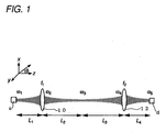
- Figure 1 is a model view of a microoptical system for explaining the microoptical system for free-space optical interconnection and its setting method of the present invention.
- rays are focused Gaussian beams.
- Figure 1 shows a point-light-source element (e.g. semiconductor laser) (hereafter referred to as a light source) s at the object space side, a first microlens 10 with a focal length f 1 , a second microlens 12 with a focal length f 2 at the image space side, and a photodetector element (hereafter referred to as a photodetector) d.
- a point-light-source element e.g. semiconductor laser
- This optical system is an imaging optical system using the first and second microlenses 10 and 12 as convex lenses.
- the image of the light source s is formed as an intermediate image by the first lens 10 and moreover, the intermediate image is formed on the light receiving plane of the photodetector d by the second imaging lens 12.
- the first and second lenses are those for image formation and referred to as imaging lens, respectively.
- ⁇ 1 represents the beam waist of Gaussian beams at a light source
- ⁇ 2 represents the effective Gaussian-beam radius on the surface of the first imaging lens 10
- ⁇ 3 represents the beam waist of Gaussian beams of the intermediate image of the light source s by the first microlens
- ⁇ 4 represents the effective Gaussian-beam radius on the surface of the second imaging lens 12
- ⁇ 5 represents the beam waist of Gaussian beams on the light receiving plane of the photodetector d.
- L 1 represents the distance between the light source s and the first imaging lens 10
- L 2 represents the distance between the first imaging lens 10 and the intermediate image
- L 3 represents the distance between the intermediate image and the second imaging lens 12
- L 4 represents the distance between the second imaging lens 12 and the light receiving plane of the photodetector d.
- the first and second microlenses described above are individual lenses respectively corresponding to a light source or photodetector one to one, which can use any one of an embossed lens, a lens made by ion exchange, and a lens using a computer generated hologram, or a compound lens.
- light-source and photodetector element groups are included in an electronic module in order to exchange optical signals together with an electronics circuit provided to process signals and drive light sources.
- Rays emitted from the light source s are Gaussian beams having a Gaussian electric-field distribution independently of whether the rays are coherent rays or incoherent rays. Therefore, actions or behavior of Gaussian beams can be described by using a ray matrix (ABCD law or ABCD matrix).
- the distances L 1 , L 2 , L 3 , and L 4 between the lenses 10 and 12 on one hand and the beam waists ⁇ 1 , ⁇ 3 , and ⁇ 5 can be obtained from the following expression (1) in accordance with a ray matrix by using the corresponding effective beam radiuses ⁇ 2 and ⁇ 4 and a light-source wavelength (light wavelength) ⁇ to be used.
- ⁇ 2 and ⁇ 4 are previously given when designing optical interconnection. That is, to connect a lot of optical systems in parallel by using the optical system in Fig. 1, there is a request value for design on the interconnection interval between the optical systems and ⁇ 2 is determined in accordance with the request value. Moreover, ⁇ 4 is determined in accordance with the degree of the influence of a positional deviation of a light source to be relaxed by the optical interconnection. Resultingly, ⁇ 3 serves as a free parameter and the interconnection length L can be regarded as a function using ⁇ 3 as a parameter.
- the maximum interconnection length Lmax corresponding to the ⁇ 3 is provided by the following expression (3).
- L 2 + L 3 ⁇ ⁇ ⁇ 2 ⁇ 4
- a interconnection length is determined by the effective beam radiuses ⁇ 2 and ⁇ 4 of the two imaging lenses 10 and 12 under the condition of the maximum interconnection length Lmax.
- the focal length f 1 of the first imaging lens 10 and the focal length f 2 of the second imaging lens 12 on the basis of the relation between the beam waists ⁇ 1 and ⁇ 5 in the light source s and photodetector d one hand and the beam waist ⁇ 3 in the intermediate image on the other.
- the forcal lengths f 1 and f 2 are obtained by using a ray matrix from the following expression (4).
- the beam waist ⁇ 3 is realized by the obtained focal length f 1 .
- the intermediate image is imaged to the image radius (beam waist) ⁇ 5 on the light receiving plane of the designated photodetector d.
- the microoptical system of the present invention has a series of relations provided by the expressions (1) to (4). Therefore, to design the microoptical system, the maximum interconnection length Lmax is first provided as a requisite.
- the beam waists ⁇ 1 and ⁇ 5 of the light source s and the photodetector d are predetermined values.
- These two effective beam radiuses ⁇ 2 and ⁇ 4 can be determined by the expression (3) by considering which values the request values for interconnection intervals should be set to and which level the positional-deviation relaxing level should be set to. Moreover, a wavelength ⁇ to be used is determined according to the light source.
- the maximum interconnection length Lmax makes it possible to select an infinite number of sets of values of the two effective beam radiuses ⁇ 2 and ⁇ 4 .
- the above-described interconnection interval that is, the distance between adjacent imaging lenses and the light-source positional-deviation-error relaxing level are requisites for limiting the number of the sets. Therefore, in the case of the present invention, ⁇ 4 is set smaller than ⁇ 2 in order to increase the tolerance of positioning errors (misalignment). At the same time, it is possible to maintain the combination length same as that of a conventional equimultiple Gaussian optical system by selecting the ratio between ⁇ 4 and ⁇ 2 in accordance with the expression (3).
- the light-source positional deviation includes a positional deviation in the optical-axis direction and a positional deviation in the direction vertical to the optical axis. Therefore, it is described below that the combination light loss due to a positioning error (misalignment) of the light source s is improved by considering these positional deviations separately and setting the effective beam radius ⁇ 4 of the second imaging lens smaller than the effective beam radius ⁇ 2 of the first imaging lens 10 in a Gaussian beam combination system used for the present invention.
- z axis of the Cartesian coordinates consisting of x, y, and z axes is the optical axis.
- the wavelength ⁇ of Gaussian beams is 1.3 ⁇ m
- the beam waist ⁇ 1 of the light source s is 2 ⁇ m
- the beam waist ⁇ 5 of the photodetector d is 5 ⁇ m
- the effective beam radius ⁇ 2 of the first imaging lens 10 is 100 ⁇ m
- the openings or apertures of the first and second imaging lenses are rectangular openings of 300 by 300 ⁇ m
- the opening of the photodetector is 15 by 15 ⁇ m in size.
- Main influences due to a positional deviation in the optical-axis direction include a power truncation (or power loss) due to the effective beam radius ⁇ 4 of the second imaging lens 12 and a power truncation due to a mismatch between the beam waist ⁇ 5 of an image converted on a light receiving plane and the detector d.
- a power truncation or power loss
- a power truncation due to a mismatch between the beam waist ⁇ 5 of an image converted on a light receiving plane and the detector d In any case, it is possible to quantitatively evaluate influences due to a positional deviation in accordance with the amount of light (or optical power or luminous energy) to be truncated (intensity of light entering the detector surface or equivalent amount of light corresponding to the light intensity) by the second imaging lens 12 and on the detector surface by using a ray matrix.
- the ratio ⁇ 4 / ⁇ 2 (this ratio is hereafter also referred to as beam spot reduction rate) is determined by using the expression (3) in accordance with the above-described design conditions and the tentatively-determined maximum interconnection length Lmax and ⁇ 3 is determined by using the expression (3) in accordance with these values. Then, the distances L 1 to L 4 and f 1 and f 2 are obtained by substituting the values ⁇ 1 to ⁇ 5 for the expressions (1) and (4) to form a designed microoptical system.
- the beam waist ⁇ 3 of an intermediate image and the distances L 2 and L 3 between the intermediate image on one hand and two imaging lenses on the other are respectively changed to ⁇ 3 ' and L 2 ' and L 3 ' due to the deviation ⁇ of the light source s in the optical-axis direction as shown in the following expression (5).
- amount of light P 1 is considered which can be transmitted through the effective area of the second imaging lens 12.
- the amount of light P 1 is a value obtained by squaring the electric field distribution of Gaussian beams, which is a value equivalent to the intensity of light entering the effective area of a lens (the effective opening of a lens is handles as a square by considering that lenses are two-dimensionally arranged on a practical system).
- the luminous energy P 1 can be obtained by surface-integrating the Gaussian distribution on the effective area of a lens. The following expression (7) is used in this case.
- a parameter is assigned to horizontal axis or abscissa as the deviation ⁇ and the result of calculating the value of the ratio ( ⁇ 4 '/ ⁇ 2 ) between the "beam radius due to deviation" ⁇ 4 ' on the second imaging lens 12 and ⁇ 2 as the beam radius ratio ( ⁇ 4 '/ ⁇ 2 ) on the second imaging lens is assigned to vertical axis or ordinate.
- ⁇ 4 ' is calculated by using the expression (6).
- the absolute value of the deviation ⁇ from the reference position gradually becomes larger than the value ( ⁇ 4 '/ ⁇ 2 ) at the reference position increases (that is, the beam radius ⁇ 4 ' due to the deviation increases) as the absolute value increases and moreover, the beam radius ratio ( ⁇ 4 '/ ⁇ 2 ) changes almost symmetrically in positive and negative directions.
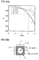
- Figure 3(A) shows the result of obtaining the amount of light (or optical power or luminous energy) P 1 based on the expression (7) by calculating a parameter as the deviation ⁇ on each of three set designed ratios ( ⁇ 4 / ⁇ 2 ).
- the deviation ⁇ is assigned to horizontal axis and the light intensity (transmitted amount of light) P 1 transmitting the second imaging lens 12 is assigned to vertical axis.
- Figure 3(B) is an illustration showing the relation between the size of the aperture or opening of the second imaging lens 12 and the "beam radius ⁇ 4 ' due to deviation".
- the beam radius ⁇ 4 ' is a value which can be obtained from the expression (6).
- Figure 3 shows that the light source is present on the origin of xy coordinates, that is, z axis (optical axis) even if it deviates in the optical-axis direction.
- the beam radius ⁇ 4 ' decreases in order of the curves c, b, and a.
- ⁇ 5 ' ⁇ 5 '' 1+ ⁇ ( L 4 - L 4 ') ⁇ 5 '' 2 2
- Amount of light P 2 received by the photodetector (also referred to as a detector) d is obtained by surface-integrating the Gaussian distribution of beams on the effective area of the light receiving plane of the photodetector ⁇ the light receiving plane is handled as a square similarly to the case of the expression (7) ⁇ and shown by the following expression (10) in the case of this embodiment.
- the already described design conditions are assumed and moreover, how the beam radius ⁇ 5 ' on the light receiving plane due to deviation of the light source in the optical axis direction changes to the designed ⁇ 5 on the already-described three designed beam spot reduction ratios ( ⁇ 4 / ⁇ 2 ) and the change of the amount of light (or optical power or luminous energy) P 2 are studied.
- straight lines a, b, and c are obtained by assigning the deviation ⁇ ( ⁇ m) of the light source s in the optical axis direction to horizontal axis and the beam radius ratio ( ⁇ 5 '/ ⁇ 5 ) of the photodetector (detector) d to vertical axis and thereby, showing the change of the beam radius of the photodetector to the deviation of the light source in the optical axis direction. From Fig. 4, it is found that the beam radius linearly changes when the light source s deviates in the optical axis direction.
- the beam radius ratio has a value of approx. 0.74 at -10 ⁇ m, a value of approx. of 1.26 at +10 ⁇ m, and a value of 1.0 at the reference position in the case of the straight line a.
- the change value of the beam radius increases as the beam spot reduction ratio of the beam radius of the second imaging lens 12 increases. That is, it is found that a focused Gaussian beam has a larger beam-radius change due to deviation of a light source contrary to the same characteristic of the second imaging lens 12.
- Figs. 5(A) and 5(B) are illustrations same as Figs. 3(A) and 3(B), showing the change of received amount of light due to the change of the beam radius shown in Fig. 4.
- the deviation ⁇ ( ⁇ m) of the light source s in the optical axis direction is assigned to horizontal axis and the amount of light (or optical power or luminous energy) P 2 received by the detector d is assigned to vertical axis.
- Figure 5(B) shows the relation between the size of the light receiving plane of the detector d and the beam radius ⁇ 5 ' on the light receiving plane.
- the beam radius ⁇ 5 ' is obtained from the expression (9).
- Fig. 3 Fig.
- Fig. 5 shows that the light source is present on the origin of the xy coordinates, that is, on z axis (optical axis) even if the light source deviates in the optical axis direction.
- Deviation of the light source s in the direction perpendicular to the optical axis causes an angle deviation and a lateral-directional axis deviation of an incoming beam on the second imaging lens 12 and the light receiving plane of the photodetector d. This study assumes that a paraxial condition is effected and ignores the angle deviation of the light source.
- ⁇ x 1 and ⁇ 1 are obtained from the following expression (11).
- amount of light (or optical power or luminous energy) P 3 transmitting the surface of the second imaging lens 12 is obtained in accordance with the axis deviation vertical to the optical axis by surface-integrating the effective area of the lens surface.
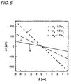
- Figure 6 is an illustration showing the axis deviation of a Gaussian beam in the direction vertical to the optical axis direction of the beam on the surface of the second imaging lens 12 by using the deviation ⁇ of the light source s in the lateral direction of the light source as a parameter to different beam spot reduction ratios on the surface of the second imaging lens. Therefore, Fig. 6 is an illustration showing a calculated deviation of the central position of the beam when it is assumed that the light source s deviates by the deviation ⁇ ( ⁇ m) in the direction vertical to its optical axis.
- the deviation ⁇ is assigned to horizontal axis and the beam shift ⁇ x 1 ( ⁇ m) on the second imaging lens is assigned to vertical axis.
- the shift ⁇ x 1 comes to approx. 50 ⁇ m, 0 ⁇ m, and approx. -50 ⁇ m when the deviation ⁇ changes from -5 ⁇ m to +5 ⁇ m centering around 0 ⁇ m in the case of the curve a.
- the shift comes to approx. 120 ⁇ m, approx. 0 ⁇ m, and approx. -120 ⁇ m correspondingly to the change of the same deviation.
- the shift comes to approx. 250 ⁇ m, 0 ⁇ m, and approx. -250 ⁇ m correspondingly to the change of the same deviation. Therefore, it is found that the change of the beam shift ⁇ x 1 to the deviation ⁇ of the light source s becomes linear and influences of beam shift can be decreased as a beam spot reduction ratio decreases.
- Figure 7(B) shows how far the center of a beam deviates from the optical axis (z axis) of the light source s on the surface of the second imaging lens 12 when the light source s deviates in the direction perpendicular to its optical axis like the case of Fig. 7(A). It is found in this example that the center of the optical axis shifts downward along x axis.
- an axis deviation ⁇ x 2 and an angle deviation ⁇ 2 on the light receiving plane can be obtained from the following expression (13) by using a ray matrix (ABCD matrix) similarly to the case of the study on the deviation ⁇ in the optical axis direction.
- Amount of light entering the light receiving plane of a detector due to the axis deviation in the direction vertical to an optical axis expressed by the expression (13) has a value obtained from the following expression (14) by surface-integrating the effective area of the light receiving plane.
- Figure 8 is an illustration showing the relation between the deviation ⁇ and the beam shift ⁇ x 2 obtained about three set beam spot reduction ratios similarly to Fig. 6 and showing the change of a beam shift on the light receiving plane due to a deviation in the direction perpendicular to the optical axis of a light source.
- the deviation ⁇ ( ⁇ m) is assigned to horizontal axis and the beam shift ⁇ x 1 ( ⁇ m) on the light receiving plane is assigned to vertical axis. From curves a, b, and c in Fig. 8, it is found that the shift ⁇ x 2 when changing ⁇ up to ⁇ 5 ⁇ m centering around 0 ⁇ m linearly changes in a range of approx.
- Figure 9(A) is an illustration showing values obtained by calculating the corresponding amount of light (or optical power or luminous energy) in accordance with the beam shift in Fig. 8 and showing the relation between the deviation ⁇ of the light source s in the direction vertical to its optical axis and incoming amount of light of beams received by the light receiving plane, that is, amount of light P 4 .
- the deviation ⁇ ( ⁇ m) is assigned to horizontal axis and the amount of light P 4 is assigned to vertical axis.
- Fig. 9(A) it is found that the tolerance of the received amount of light P 4 decreases correspondingly to the deviation ⁇ by increasing the beam spot reduation ratio of the beam radius (from the curve c to the curve a). However, it is found that the decrease of the tolerance is up to approx. 5% in the range of the change of the deviation ⁇ . Moreover, though a focused Gaussian beam is more sensitive to a lateral deviation of a light source, it is possible to select an optimum condition by properly selecting a beam spot reduction ratio.
- Figure 9(B) shows how far the center of a beam deviates from the optical axis (z axis) on the light receiving plane of the photodetector d when the light source s deviates in the direction perpendicular to its optical axis. From this example, it is found that the center shifts upward (positive direction) along x axis differently from the deviation direction in Fig. 7(B).
- the power loss resulting from a beam shift due to a lateral-directional deviation of the light source is the biggest problem in the case of the second imaging lens. That is, it is estimated that the lateral deviation of the light source vertical to the optical axis has the biggest influence.
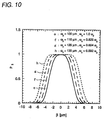
- Fig. 10 shows the result of calculating the amount of light (or optical power or luminous energy) transmitting the second imaging lens due to the lateral-directional deviation of a light source on various focused Gaussian beams obtained by keeping the interconnection length constant and changing combinations of beam radiuses of two imaging lenses.
- the lateral-directional deviation ⁇ ( ⁇ m) from the optical axis of a light source is assigned to x axis and amount of light (or optical power or luminous energy) P 5 transmitting the second imaging lens is assigned to y axis.
- the curve e is obtained by setting ⁇ 2 to 100 ⁇ m and ⁇ 4 to 1.0 ⁇ 2
- the curve f is obtained by setting ⁇ 2 to 110 ⁇ m and ⁇ 4 to 0.826 ⁇ 2
- the curve g is obtained by setting ⁇ 2 to 120 ⁇ m and ⁇ 4 to 0.694 ⁇ 2
- the curve h is obtained by setting ⁇ 2 to 130 ⁇ m and ⁇ 4 to 0.592 ⁇ 2 .
- the microoptical system for free-space optical interconnection and its setting method of the present invention use focused Gaussian beams and thereby position a point-light-source element, a first microlens, a second microlens, and a photodetector element so that an effective radius ⁇ 2 of a focused Gaussian beam on the first microlens is set larger than an effective radius ⁇ 4 of a focused Gaussian beam on the second microlens.
- the microoptical system and its setting method of the present invention can preferably be applied to the free-space optical interconnection of a packaged optical-system module in which a light source and a photodetector arranged on a glass substrate and the light source and photo detector are optically combined by focused Gaussian beams and lenses so that information processing can be performed.
Landscapes
- Physics & Mathematics (AREA)
- General Physics & Mathematics (AREA)
- Optics & Photonics (AREA)
- Length Measuring Devices By Optical Means (AREA)
- Optical Couplings Of Light Guides (AREA)
- Semiconductor Lasers (AREA)
Applications Claiming Priority (4)
| Application Number | Priority Date | Filing Date | Title |
|---|---|---|---|
| JP159561/95 | 1995-06-26 | ||
| JP15956195 | 1995-06-26 | ||
| JP312398/95 | 1995-11-30 | ||
| JP7312398A JPH0973041A (ja) | 1995-06-26 | 1995-11-30 | 自由空間光配線用のマイクロ光学系およびそのセッティング方法 |
Publications (1)
| Publication Number | Publication Date |
|---|---|
| EP0753776A1 true EP0753776A1 (fr) | 1997-01-15 |
Family
ID=26486315
Family Applications (1)
| Application Number | Title | Priority Date | Filing Date |
|---|---|---|---|
| EP96110314A Withdrawn EP0753776A1 (fr) | 1995-06-26 | 1996-06-26 | Système microoptique pour interconnexion optique en espace libre et son procédé d'ajustement |
Country Status (3)
| Country | Link |
|---|---|
| US (1) | US5986788A (fr) |
| EP (1) | EP0753776A1 (fr) |
| JP (1) | JPH0973041A (fr) |
Families Citing this family (14)
| Publication number | Priority date | Publication date | Assignee | Title |
|---|---|---|---|---|
| US7128737B1 (en) * | 1997-10-22 | 2006-10-31 | Carl Zeiss Meditec Ag | Object figuring device |
| US6694101B1 (en) * | 1998-12-31 | 2004-02-17 | Worldcom, Inc. | Focal plane division multiplexing system and method |
| US6580845B1 (en) | 2000-08-11 | 2003-06-17 | General Nutronics, Inc. | Method and device for switching wavelength division multiplexed optical signals using emitter arrays |
| US7279674B2 (en) * | 2000-08-17 | 2007-10-09 | Avago Technologies Ecbu Ip (Singapore) Pte Ltd | Optical encoder module |
| JP2002243991A (ja) * | 2001-02-15 | 2002-08-28 | Nippon Sheet Glass Co Ltd | 結合光学系およびそれを用いた光学素子 |
| US7978981B2 (en) * | 2002-02-22 | 2011-07-12 | Avago Technologies Fiber Ip (Singapore) Pte. Ltd. | Structure and apparatus for a very short haul, free space, and fiber optic interconnect and data link |
| US7302181B2 (en) * | 2003-02-25 | 2007-11-27 | Avago Technologies Ecbu Ip (Singapore) Pte. Ltd. | Single lens multiple light source device |
| US8244134B2 (en) * | 2007-06-19 | 2012-08-14 | Charles Santori | Optical interconnect |
| WO2009096927A1 (fr) * | 2008-01-31 | 2009-08-06 | Hewlett-Packard Development Company, L.P. | Interconnexion optique en espace libre |
| ES2487621T3 (es) * | 2009-05-06 | 2014-08-22 | Tesat Spacecom Gmbh & Co. Kg | Dispositivo híbrido de comunicación para una transmisión de datos de alta velocidad entre plataformas móviles y/o plataformas estacionarias |
| US10411812B1 (en) * | 2013-03-15 | 2019-09-10 | Forrest Rose | Optical interconnect computing module tolerant to changes in position and orientation |
| US9413448B2 (en) * | 2014-08-08 | 2016-08-09 | Nxgen Partners Ip, Llc | Systems and methods for focusing beams with mode division multiplexing |
| EP3980846A1 (fr) * | 2019-06-06 | 2022-04-13 | Optalysys Ltd | Dispositifs de guides d'ondes |
| CN115113344A (zh) * | 2021-03-18 | 2022-09-27 | 富士康(昆山)电脑接插件有限公司 | 无接触式连接器及其组件 |
Citations (2)
| Publication number | Priority date | Publication date | Assignee | Title |
|---|---|---|---|---|
| EP0463390A2 (fr) * | 1990-06-22 | 1992-01-02 | International Business Machines Corporation | Connecteurs électro-optiques |
| EP0560511A2 (fr) * | 1992-03-09 | 1993-09-15 | AT&T Corp. | Agencement d'interconnexion optique en libre espace |
Family Cites Families (2)
| Publication number | Priority date | Publication date | Assignee | Title |
|---|---|---|---|---|
| US5532856A (en) * | 1994-06-30 | 1996-07-02 | Nec Research Institute, Inc. | Planar optical mesh-connected tree interconnect network |
| US5568574A (en) * | 1995-06-12 | 1996-10-22 | University Of Southern California | Modulator-based photonic chip-to-chip interconnections for dense three-dimensional multichip module integration |
-
1995
- 1995-11-30 JP JP7312398A patent/JPH0973041A/ja not_active Withdrawn
-
1996
- 1996-06-25 US US08/670,356 patent/US5986788A/en not_active Expired - Fee Related
- 1996-06-26 EP EP96110314A patent/EP0753776A1/fr not_active Withdrawn
Patent Citations (2)
| Publication number | Priority date | Publication date | Assignee | Title |
|---|---|---|---|---|
| EP0463390A2 (fr) * | 1990-06-22 | 1992-01-02 | International Business Machines Corporation | Connecteurs électro-optiques |
| EP0560511A2 (fr) * | 1992-03-09 | 1993-09-15 | AT&T Corp. | Agencement d'interconnexion optique en libre espace |
Non-Patent Citations (5)
| Title |
|---|
| F.B.MCCORMICK ET.AL.: "oPTICAL INTERCONNECTIONS USING MICROLENS ARRAYS", OPTICAL AND QUANTUM ELECTRONICS, vol. 24, no. 4, April 1992 (1992-04-01), LONDON, pages 465 - 477, XP000431185 * |
| JAHNS J ET AL: "PARALLEL OPTICAL INTERCONNECTIONS USING SURFACE-EMITTING MICROLASERS AND A HYBRID IMAGING SYSTEM", OPTICS COMMUNICATIONS, vol. 109, no. 3/04, 1 July 1994 (1994-07-01), pages 328 - 337, XP000448151 * |
| KOSTUK R K ET AL: "DISTRIBUTED OPTICAL DATA BUS FOR BOARD-LEVEL INTERCONNECTS", APPLIED OPTICS, vol. 32, no. 26, 10 September 1993 (1993-09-10), pages 5010 - 5021, XP000393401 * |
| SAUER F ET AL: "REFRACTIVE-DIFFRACTIVE MICRO-OPTICS FOR PERMUTATION INTERCONNECTS", OPTICAL ENGINEERING, vol. 33, no. 5, 1 May 1994 (1994-05-01), pages 1550 - 1560, XP000440831 * |
| YASUTOSHI YAGIU ET AL: "NEW COLLIMATING LENS SYSTEM FOR LASER DIODE PACKAGE", PROCEEDINGS OF THE ELECTRONIC COMPONENTS AND TECHNOLOGY CONFERENCE, ORLANDO, JUNE 1 - 4, 1993, no. CONF. 43, 1 June 1993 (1993-06-01), INSTITUTE OF ELECTRICAL AND ELECTRONICS ENGINEERS, pages 1135 - 1138, XP000380114 * |
Also Published As
| Publication number | Publication date |
|---|---|
| US5986788A (en) | 1999-11-16 |
| JPH0973041A (ja) | 1997-03-18 |
Similar Documents
| Publication | Publication Date | Title |
|---|---|---|
| EP0619505B1 (fr) | Réseau de collimateurs optiques et méthode d'alignement de ses axes optiques | |
| EP0753776A1 (fr) | Système microoptique pour interconnexion optique en espace libre et son procédé d'ajustement | |
| US10451805B2 (en) | Wavelength division multiplexing/demultiplexing optical transceiving assembly based on diffraction grating | |
| US5428704A (en) | Optoelectronic interface and method of making | |
| US5853626A (en) | Optical module and a fabrication process thereof | |
| US6456761B2 (en) | Apparatus, assembly, and method for making micro-fixtured lensed assembly for optoelectronic devices and optical fibers | |
| EP0477036A2 (fr) | Dispositif pour la transmission d'informations optiques | |
| US6766076B2 (en) | Optical module and method for assembling the same | |
| DE19742895C2 (de) | Elektrooptische Anordnung | |
| DE102016221806B4 (de) | Wellenlängen-Multiplexeinheit, Wellenlängen-Multiplexsystem und Verfahren zum Bilden einer Wellenlängen-Multiplexeinheit | |
| US6326939B1 (en) | Optical waveguide system for a flat-panel display | |
| US7167618B2 (en) | Optical module having stacked guide substrates and method for assembling the same | |
| Kim et al. | Three-dimensionally interconnected multi-bus-line bidirectional optical backplane | |
| CN108614333B (zh) | 一种超小间距光滤波器组件结构及其制作方法 | |
| CN111025485B (zh) | 一种基于阵列波导光栅技术的波分复用光组件 | |
| Zhao et al. | Hybrid optoelectronic backplane bus for multiprocessor-based computing systems | |
| Oikawa et al. | Light coupling characteristics of planar microlens | |
| EP3422614A1 (fr) | Dispositif de multiplexage par répartition en longueur d'onde optique | |
| JP3915942B2 (ja) | 自由空間光配線用光学レンズ装置 | |
| EP4024103A1 (fr) | Module optique et système de réseau de communication optique l'utilisant | |
| DE202024101454U1 (de) | Lichtstrahlaufweitungssystem und optoelektronische Vorrichtung | |
| CN109669249B (zh) | 一种双波长双向传输光组件及方法 | |
| TW202607407A (zh) | 用於具有經打線接合部件之光學互連模組中之個別界定的光學元件 | |
| WO2025123008A1 (fr) | Coupleurs d'imagerie pour liaisons à micro-del | |
| Sasaki et al. | Passive alignment technique for single-channel laser diode coupling to single-mode fiber on v-grooved Si waferboard |
Legal Events
| Date | Code | Title | Description |
|---|---|---|---|
| PUAI | Public reference made under article 153(3) epc to a published international application that has entered the european phase |
Free format text: ORIGINAL CODE: 0009012 |
|
| AK | Designated contracting states |
Kind code of ref document: A1 Designated state(s): DE FR GB |
|
| 17P | Request for examination filed |
Effective date: 19970707 |
|
| STAA | Information on the status of an ep patent application or granted ep patent |
Free format text: STATUS: THE APPLICATION HAS BEEN WITHDRAWN |
|
| 18W | Application withdrawn |
Withdrawal date: 19990203 |