EP0754976B1 - Procédé pour l'activiation d'une surface ainsi que appareil et lampe pour exécuter ce procédé - Google Patents
Procédé pour l'activiation d'une surface ainsi que appareil et lampe pour exécuter ce procédé Download PDFInfo
- Publication number
- EP0754976B1 EP0754976B1 EP96111119A EP96111119A EP0754976B1 EP 0754976 B1 EP0754976 B1 EP 0754976B1 EP 96111119 A EP96111119 A EP 96111119A EP 96111119 A EP96111119 A EP 96111119A EP 0754976 B1 EP0754976 B1 EP 0754976B1
- Authority
- EP
- European Patent Office
- Prior art keywords
- workpiece
- lamp
- mask
- encapsulated
- ultraviolet light
- Prior art date
- Legal status (The legal status is an assumption and is not a legal conclusion. Google has not performed a legal analysis and makes no representation as to the accuracy of the status listed.)
- Expired - Lifetime
Links
- 238000000034 method Methods 0.000 title claims description 20
- 230000008569 process Effects 0.000 title claims description 18
- 230000003213 activating effect Effects 0.000 title description 8
- 230000000007 visual effect Effects 0.000 claims description 37
- 239000007789 gas Substances 0.000 claims description 34
- QSHDDOUJBYECFT-UHFFFAOYSA-N mercury Chemical compound [Hg] QSHDDOUJBYECFT-UHFFFAOYSA-N 0.000 claims description 32
- 229910052753 mercury Inorganic materials 0.000 claims description 32
- 229910052793 cadmium Inorganic materials 0.000 claims description 23
- BDOSMKKIYDKNTQ-UHFFFAOYSA-N cadmium atom Chemical compound [Cd] BDOSMKKIYDKNTQ-UHFFFAOYSA-N 0.000 claims description 23
- 230000003287 optical effect Effects 0.000 claims description 13
- 230000001678 irradiating effect Effects 0.000 claims description 12
- QVGXLLKOCUKJST-UHFFFAOYSA-N atomic oxygen Chemical compound [O] QVGXLLKOCUKJST-UHFFFAOYSA-N 0.000 claims description 10
- 239000001301 oxygen Substances 0.000 claims description 10
- 229910052760 oxygen Inorganic materials 0.000 claims description 10
- 238000001816 cooling Methods 0.000 claims description 9
- VYPSYNLAJGMNEJ-UHFFFAOYSA-N Silicium dioxide Chemical compound O=[Si]=O VYPSYNLAJGMNEJ-UHFFFAOYSA-N 0.000 claims description 6
- 230000008878 coupling Effects 0.000 claims 5
- 238000010168 coupling process Methods 0.000 claims 5
- 238000005859 coupling reaction Methods 0.000 claims 5
- 239000012141 concentrate Substances 0.000 claims 2
- 239000004973 liquid crystal related substance Substances 0.000 description 25
- 239000000758 substrate Substances 0.000 description 22
- 238000005538 encapsulation Methods 0.000 description 14
- 210000002858 crystal cell Anatomy 0.000 description 13
- 230000004913 activation Effects 0.000 description 9
- 239000010409 thin film Substances 0.000 description 8
- 230000005855 radiation Effects 0.000 description 7
- 230000002411 adverse Effects 0.000 description 6
- 230000003595 spectral effect Effects 0.000 description 6
- 238000012216 screening Methods 0.000 description 3
- XKRFYHLGVUSROY-UHFFFAOYSA-N Argon Chemical compound [Ar] XKRFYHLGVUSROY-UHFFFAOYSA-N 0.000 description 2
- PEDCQBHIVMGVHV-UHFFFAOYSA-N Glycerol Natural products OCC(O)CO PEDCQBHIVMGVHV-UHFFFAOYSA-N 0.000 description 2
- 230000005540 biological transmission Effects 0.000 description 2
- OKIIEJOIXGHUKX-UHFFFAOYSA-L cadmium iodide Chemical compound [Cd+2].[I-].[I-] OKIIEJOIXGHUKX-UHFFFAOYSA-L 0.000 description 2
- 210000004027 cell Anatomy 0.000 description 2
- 230000008859 change Effects 0.000 description 2
- 238000010276 construction Methods 0.000 description 2
- 230000007423 decrease Effects 0.000 description 2
- 230000003247 decreasing effect Effects 0.000 description 2
- 230000006866 deterioration Effects 0.000 description 2
- 239000007788 liquid Substances 0.000 description 2
- 238000004519 manufacturing process Methods 0.000 description 2
- LWJROJCJINYWOX-UHFFFAOYSA-L mercury dichloride Chemical compound Cl[Hg]Cl LWJROJCJINYWOX-UHFFFAOYSA-L 0.000 description 2
- 229920002120 photoresistant polymer Polymers 0.000 description 2
- 230000009467 reduction Effects 0.000 description 2
- 229910052774 Proactinium Inorganic materials 0.000 description 1
- 230000002159 abnormal effect Effects 0.000 description 1
- 230000009471 action Effects 0.000 description 1
- 230000004075 alteration Effects 0.000 description 1
- 238000013459 approach Methods 0.000 description 1
- 229910052786 argon Inorganic materials 0.000 description 1
- 230000000694 effects Effects 0.000 description 1
- 239000010408 film Substances 0.000 description 1
- 150000004820 halides Chemical class 0.000 description 1
- 229910052736 halogen Inorganic materials 0.000 description 1
- 150000002367 halogens Chemical class 0.000 description 1
- 238000005286 illumination Methods 0.000 description 1
- 239000011159 matrix material Substances 0.000 description 1
- 229960002523 mercuric chloride Drugs 0.000 description 1
- YFDLHELOZYVNJE-UHFFFAOYSA-L mercury diiodide Chemical compound I[Hg]I YFDLHELOZYVNJE-UHFFFAOYSA-L 0.000 description 1
- 229910052751 metal Inorganic materials 0.000 description 1
- 239000002184 metal Substances 0.000 description 1
- 231100000989 no adverse effect Toxicity 0.000 description 1
- 229920001721 polyimide Polymers 0.000 description 1
- 239000009719 polyimide resin Substances 0.000 description 1
- 230000002035 prolonged effect Effects 0.000 description 1
- 239000004065 semiconductor Substances 0.000 description 1
- 230000006641 stabilisation Effects 0.000 description 1
- 238000011105 stabilization Methods 0.000 description 1
Images



Classifications
-
- G—PHYSICS
- G02—OPTICS
- G02F—OPTICAL DEVICES OR ARRANGEMENTS FOR THE CONTROL OF LIGHT BY MODIFICATION OF THE OPTICAL PROPERTIES OF THE MEDIA OF THE ELEMENTS INVOLVED THEREIN; NON-LINEAR OPTICS; FREQUENCY-CHANGING OF LIGHT; OPTICAL LOGIC ELEMENTS; OPTICAL ANALOGUE/DIGITAL CONVERTERS
- G02F1/00—Devices or arrangements for the control of the intensity, colour, phase, polarisation or direction of light arriving from an independent light source, e.g. switching, gating or modulating; Non-linear optics
- G02F1/01—Devices or arrangements for the control of the intensity, colour, phase, polarisation or direction of light arriving from an independent light source, e.g. switching, gating or modulating; Non-linear optics for the control of the intensity, phase, polarisation or colour
- G02F1/13—Devices or arrangements for the control of the intensity, colour, phase, polarisation or direction of light arriving from an independent light source, e.g. switching, gating or modulating; Non-linear optics for the control of the intensity, phase, polarisation or colour based on liquid crystals, e.g. single liquid crystal display cells
- G02F1/133—Constructional arrangements; Operation of liquid crystal cells; Circuit arrangements
- G02F1/1333—Constructional arrangements; Manufacturing methods
- G02F1/1337—Surface-induced orientation of the liquid crystal molecules, e.g. by alignment layers
-
- G—PHYSICS
- G03—PHOTOGRAPHY; CINEMATOGRAPHY; ANALOGOUS TECHNIQUES USING WAVES OTHER THAN OPTICAL WAVES; ELECTROGRAPHY; HOLOGRAPHY
- G03F—PHOTOMECHANICAL PRODUCTION OF TEXTURED OR PATTERNED SURFACES, e.g. FOR PRINTING, FOR PROCESSING OF SEMICONDUCTOR DEVICES; MATERIALS THEREFOR; ORIGINALS THEREFOR; APPARATUS SPECIALLY ADAPTED THEREFOR
- G03F7/00—Photomechanical, e.g. photolithographic, production of textured or patterned surfaces, e.g. printing surfaces; Materials therefor, e.g. comprising photoresists; Apparatus specially adapted therefor
- G03F7/70—Microphotolithographic exposure; Apparatus therefor
- G03F7/70216—Mask projection systems
- G03F7/7035—Proximity or contact printers
-
- G—PHYSICS
- G03—PHOTOGRAPHY; CINEMATOGRAPHY; ANALOGOUS TECHNIQUES USING WAVES OTHER THAN OPTICAL WAVES; ELECTROGRAPHY; HOLOGRAPHY
- G03F—PHOTOMECHANICAL PRODUCTION OF TEXTURED OR PATTERNED SURFACES, e.g. FOR PRINTING, FOR PROCESSING OF SEMICONDUCTOR DEVICES; MATERIALS THEREFOR; ORIGINALS THEREFOR; APPARATUS SPECIALLY ADAPTED THEREFOR
- G03F7/00—Photomechanical, e.g. photolithographic, production of textured or patterned surfaces, e.g. printing surfaces; Materials therefor, e.g. comprising photoresists; Apparatus specially adapted therefor
- G03F7/20—Exposure; Apparatus therefor
- G03F7/2002—Exposure; Apparatus therefor with visible light or UV light, through an original having an opaque pattern on a transparent support, e.g. film printing, projection printing; by reflection of visible or UV light from an original such as a printed image
- G03F7/2004—Exposure; Apparatus therefor with visible light or UV light, through an original having an opaque pattern on a transparent support, e.g. film printing, projection printing; by reflection of visible or UV light from an original such as a printed image characterised by the use of a particular light source, e.g. fluorescent lamps or deep UV light
-
- G—PHYSICS
- G03—PHOTOGRAPHY; CINEMATOGRAPHY; ANALOGOUS TECHNIQUES USING WAVES OTHER THAN OPTICAL WAVES; ELECTROGRAPHY; HOLOGRAPHY
- G03F—PHOTOMECHANICAL PRODUCTION OF TEXTURED OR PATTERNED SURFACES, e.g. FOR PRINTING, FOR PROCESSING OF SEMICONDUCTOR DEVICES; MATERIALS THEREFOR; ORIGINALS THEREFOR; APPARATUS SPECIALLY ADAPTED THEREFOR
- G03F7/00—Photomechanical, e.g. photolithographic, production of textured or patterned surfaces, e.g. printing surfaces; Materials therefor, e.g. comprising photoresists; Apparatus specially adapted therefor
- G03F7/70—Microphotolithographic exposure; Apparatus therefor
- G03F7/708—Construction of apparatus, e.g. environment aspects, hygiene aspects or materials
- G03F7/70858—Environment aspects, e.g. pressure of beam-path gas, temperature
- G03F7/70866—Environment aspects, e.g. pressure of beam-path gas, temperature of mask or workpiece
-
- G—PHYSICS
- G02—OPTICS
- G02F—OPTICAL DEVICES OR ARRANGEMENTS FOR THE CONTROL OF LIGHT BY MODIFICATION OF THE OPTICAL PROPERTIES OF THE MEDIA OF THE ELEMENTS INVOLVED THEREIN; NON-LINEAR OPTICS; FREQUENCY-CHANGING OF LIGHT; OPTICAL LOGIC ELEMENTS; OPTICAL ANALOGUE/DIGITAL CONVERTERS
- G02F1/00—Devices or arrangements for the control of the intensity, colour, phase, polarisation or direction of light arriving from an independent light source, e.g. switching, gating or modulating; Non-linear optics
- G02F1/01—Devices or arrangements for the control of the intensity, colour, phase, polarisation or direction of light arriving from an independent light source, e.g. switching, gating or modulating; Non-linear optics for the control of the intensity, phase, polarisation or colour
- G02F1/13—Devices or arrangements for the control of the intensity, colour, phase, polarisation or direction of light arriving from an independent light source, e.g. switching, gating or modulating; Non-linear optics for the control of the intensity, phase, polarisation or colour based on liquid crystals, e.g. single liquid crystal display cells
- G02F1/133—Constructional arrangements; Operation of liquid crystal cells; Circuit arrangements
- G02F1/1333—Constructional arrangements; Manufacturing methods
- G02F1/1337—Surface-induced orientation of the liquid crystal molecules, e.g. by alignment layers
- G02F1/13378—Surface-induced orientation of the liquid crystal molecules, e.g. by alignment layers by treatment of the surface, e.g. embossing, rubbing or light irradiation
- G02F1/133788—Surface-induced orientation of the liquid crystal molecules, e.g. by alignment layers by treatment of the surface, e.g. embossing, rubbing or light irradiation by light irradiation, e.g. linearly polarised light photo-polymerisation
Definitions
- the invention relates to a surface irradiation process which is used to improve the surface characteristic.
- liquid crystal display devices there is, on the one hand, a liquid crystal display device of the transmission type, which is formed of a liquid crystal panel, a driver to control the latter, and a back light.
- a liquid crystal display device of the reflection type which does not use back light, but internal lighting.
- a liquid crystal cell conventionally consists of two substrates. On one of these substrates, a driver system for triggering the liquid crystals, such as a thin-film transistor, and electrodes for triggering the liquid crystals, as well as an alignment layer for alignment of liquid crystals to a certain direction, are formed. A light screening film which is called a black matrix is formed on the other of these substrates. In a color liquid crystal cell, a color filter and the above described alignment layer are formed.
- the alignment layer is produced by subjecting one surface of a thin film, such as polyimide resin or the like, to a treatment which is called rubbing, and by providing it with fine grooves (scratches) in a certain direction; this is intended to align the molecules of the liquid crystal along these fine grooves in a certain direction.
- a thin film such as polyimide resin or the like
- the picture contrast changes according to the angle of view field.
- the angular range in which advantageous contrast is obtained is called the angle of view field of the liquid crystal cell.
- the greater this angle of view field the more visible and better the liquid crystal cell becomes. Therefore, there is the important technical object of how a large visual angle is obtained.
- a pre-tilt angle of the molecules of the liquid crystals is controlled.
- the term "pre-tilt angle” is defined as an angle for which the molecules of the liquid crystals with reference to the surface of the alignment layer rise with a certain angle when they come into contact with the alignment layer.
- the alignment layer is irradiated through a mask with ultraviolet light, and thus, the characteristic of the alignment layer is activated.
- This technique of controlling the pre-tilt angle is known, for example, from Japanese patent disclosure document HEI 6-222366 and Japanese patent disclosure document HEI 6-281937.
- a liquid crystal cell with a wide angle of view field is produced using the phenomenon that the pre-tilt angle of the areas irradiated with the ultraviolet light decreases and using the measure by which, within this same substrate, areas with different pre-tilt angles are arranged in mixed fashion.
- the phenomenon that the pre-tilt angle is changed by irradiation with ultraviolet light is presumably caused by the fact that the surface of the alignment layer is oxidized by the ultraviolet light and that the polarity of the alignment layer changes.
- To activate the above described alignment layer it is necessary to place the alignment layer within a gas atmosphere which contains oxygen when it is irradiated with ultraviolet light. This means that, in irradiation of the alignment layer with ultraviolet light through the mask, the mask and the surface of the alignment layer (substrate surface) are held at a distance from one another and a gas layer (air) which contains oxygen is formed between the mask and alignment layer.
- US 4,023,904 A describes a process for exposing a semiconductor substrate coated with a photoresist to ultraviolet light having a wavelength in the range of from 300 to 500 nm.
- the UV light is passed through lenticules such that the radiation approaches the mask opening from different angles generating slightly superposed diffraction patterns.
- the purpose of this arrangement is more uniform illumination of the photoresist.
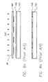
- Fig. 8 is a schematic of the known process for activating the characteristic of the alignment layer by irradiation with ultraviolet light in the above described manner.
- a mask pattern MP is formed which partially screens the ultraviolet light.
- the above described thin-film transistor, the above described electrodes for triggering of the liquid crystals and the like, which are not shown in the drawing, are formed and on which alignment layer 102 is formed.
- the mask MK, on which the mask pattern MP is formed is positioned at a distance from the substrate 101 on which alignment layer 102 is formed, and the mask MK is irradiated with ultraviolet light from above.
- the characteristic of alignment layer 102 is partially activated and the pre-tilt angle of the areas irradiated with the ultraviolet light changes.
- ultraviolet light with wavelengths of less than or equal to 300 nm (especially from 200 nm to 300 nm) é can be used.
- a mercury lamp of the long arc type is known as a light source which emits light in this wavelength range. The reason for this is that the distance between the discharge electrodes is great, i.e., it is a few dozen cm to a few hundred cm, that the surface of the emission part is large, and that therefore strong ultraviolet light is easily obtained.
- a mercury lamp of the long arc type is known as a lamp which is used to activate the characteristic of the alignment layer or the like which is formed on the substrate.
- the substrate is called a workpiece.
- the ultraviolet light from a lamp of this type is, however, scattered light.
- a lamp is used with an arc length such as in a mercury lamp of the long arc type or the like, using a lens with a high degree of parallelism of the central light beam, the degree of parallelism of the light emitted from the middle area of the lamp can be increased.
- the light which is emitted from the end of the lamp is, however, obliquely incident on the workpiece, this angle being designated the visual angle.
- the visual angle is defined as a half angle with consideration of a light source. As a result thereof, advantageous parallel light is not obtained and the oblique light enters.
- a lamp with a large arc length has a large discharge surface.
- an integrator lens or the like it is necessary to enlarge this integrator lens. This leads to the disadvantage of resultant higher costs.
- the "arc length" is equivalent to the distance between the electrodes of the lamp.
- a lamp is used with a short arc length, such as a super high pressure mercury lamp or the like, the degree of parallelism of the light can be increased and the visual angle can be decreased. If the visual angle is extremely decreased, light diffraction phaenomenon occurs more. As a result, the exposure of the screened parts increases due to the diffracted light.
- a lamp with a short arc length is constructed such that the light with a so-called i-line (365 nm), an h-line (405 nm) and a g-line (436 nm) is emitted with high efficiency. Radiation of the above described ultraviolet light with wavelengths of less than or equal to 300 nm is low in this case. In a lamp with a low arc length (discharge lamp of the short arc type), therefore, in the wavelength range which is necessary for activating the surface of the alignment layer, an irradiance in a sufficient amount cannot be obtained. In addition, when used as a surface activation lamp, it is considered disadvantageous that the duration of irradiation becomes long.
- a first object of the invention is to devise a surface irradiation process in which entry of adverse light (oblique light and diffracted light) can be prevented and in which irradiation of undesired areas does not occur.
- a second object of the invention is to devise an advantageous light source for purposes of surface irradiation as well as a device, which is suitable for implementing irradiation of a thin film which is formed on the workpiece, in which the workpiece is irradiated with light through the mask which is located at a distance from the workpiece, such as for implementing irradiation of an alignment layer on a substrate of liquid crystal cell or the like.
- a third object of the invention to devise a lamp for purposes of surface irradiation in which a high irradiance is obtained in the wavelength range which is necessary for surface irradiation, and in which surface irradiation can be achieved within a short period of time.
- the diffraction of light increases and the amount of light which enters due to diffraction becomes greater when the visual angle ⁇ is too small. It is conceivable that the size of the visual angle ⁇ at which, due to the above described light diffraction, entry of the diffracted light occurs is less than or equal to 1.5° .
- the visual angle ⁇ is too large, the light is incident obliquely on the mask and undesired areas are irradiated, as was described above.
- the maximum value of above described visual angle ⁇ can be computed in the manner described below. This means that, if the width of entry of the adverse light is less than or equal to 1/10 of width W of the smallest part of the areas to be irradiated, in practice, no adverse effect is exerted on the picture of the liquid crystal cell, and therefore, it can be acceptable.
- the width of entry of the adverse light is, furthermore, represented by a function between thickness d of the gas layer (the distance between the mask and the workpiece) and the visual angle ⁇ of the light.
- the maximum value ⁇ max of the visual angle can, therefore, be denoted with the following formula: d x tan ⁇ max ⁇ 0.1 W
- thickness d of the gas layer is 10 ⁇ m (microns) and furthermore width W of the areas of the alignment layer to be activated is likewise 100 ⁇ m (microns), as was described above, the maximum value ⁇ max of the visual angle is roughly 5.7° .
- visual angle ⁇ is within the range described below, if the workpiece is irradiated with light through the mask which is located at a distance to the workpiece and if surface irradiation is performed with it: 1.5° ⁇ ⁇ ⁇ ⁇ max (roughly 5.7°)
- Visual angle ⁇ depends on the arc length of the lamp, as was described above. If the arc length of the lamp is great, visual angle ⁇ becomes greater while, at a small arc length, the visual angle a becomes smaller. This means that it is necessary to select the arc length of the lamp accordingly in a suitable manner in order that visual angle ⁇ can be within a certain range.
- an arc length is computed at which visual angle ⁇ is within the above described range, as is described below.
- the arc length is roughly 7.5 mm to obtain a visual angle of 1.5° and that the arc length is roughly 29 mm to obtain a visual angle of 5.7° .
- a lamp for performing surface irradiation in which a workpiece is irradiated with light through a mask which is located at a distance to the workpiece as for irradiation of an alignment layer on a substrate of a liquid crystal cell or the like, a lamp with an arc length of roughly 7.5 mm to 29 mm is, therefore, desired.
- ultraviolet light with wavelengths from 200 nm to 300 nm is useful as was described above. Furthermore, for surface irradiation of an alignment layer on a substrate of a liquid crystal cell or the like under the above described ultraviolet light, ultraviolet light with wavelengths from 200 to 230 nm is more effective than ultraviolet light with wavelength from 230 to 300 nm. (Ultraviolet light with wavelengths from 200 nm to 230 nm has at least twice the action as ultraviolet light with wavelengths from 230 nm to 300 nm. Therefore, the duration of treatment is only less than or equal to half.)
- Figure 5 shows a case in which the power input into the lamp arc (power at which the loss, as in a voltage drop of the electrodes or the like, was subtracted from the lamp input power) was kept constant.
- a spectrometer was used, which was calibrated using a standard lamp (model UV-40 manufactured by Optronic Laboratories, Inc.), to measure the relative spectral distribution of the lamp in the horizontal direction from a distance of 1 m; this was denoted the total radiant energy by multiplication by 4 ⁇ .
- the encapsulation pressure of the rare gas in the case of use as a lamp for purposes of activating the thin layer, is 0.1 x 10 5 to 5 x 10 5 (Pa), as is apparent from Fig. 5.
- the irradiance increases, the smaller the encapsulation pressure of the rare gas.
- an encapsulation pressure of the rare gas of less than or equal to 0.05 x 10 5 Pa when the lamp is ignited, no arc was formed by the anode tip, and an abnormal arc formed. It is, therefore, necessary for stabilization of the igniting characteristic that the encapsulation pressure of the rare gas be greater than or equal to 0.1 x 10 5 Pa.
- Fig. 7 shows a case in which the power input into the lamp arc was kept constant, as in Fig. 5. This result showed that as a lamp for purposes of irradiating a thin film, it is desirable that the amount of cadmium C (mg/cm 3 (cc)) is in the range of 0.06 ⁇ C ⁇ 3.
- encapsulation pressure P2 of the rare gas in the cadmium lamp in the case of use as a lamp for purposes of activating the thin film, is 0.1 x 10 5 to 3 x 10 6 Pa, as becomes apparent from Fig. 7.
- the irradiance increases, the greater the encapsulation pressure of the rare gas.
- encapsulation pressure P2 be less than or equal to 3 x 10 6 Pa.
- the mercury lamp has less ultraviolet light with wavelengths from 200 nm to 230 nm than the cadmium lamp, as was described above.
- the amount of mercury M Q (mg/cm 3 (cc)) is within the range of 2 ⁇ M Q ⁇ 15, and in which, also, the encapsulation pressure P1 (Pa) of the rare gas is in the range from 0.1 x 10 5 ⁇ P1 ⁇ 5 x 10 5 , however, an irradiance in an amount sufficient for surface irradiation is obtained. Therefore the mercury lamp according to the invention can be used to a sufficient degree for practical purposes.
- the intensity of the light emitted from the lamp was checked.
- the intensity of the emitted light is greater, the greater the power supplied to the arc (the power which contributes to emission).
- the upper limit of the current I depends on the electrode configuration of the lamp, the cooling efficiency of the lamp and the like. Moreover, at an overly large current, damage to the electrodes is more possible, and efficiency drops as a result of a voltage drop on the electrodes or the like. The upper boundary is, therefore, necessarily fixed and cannot be easily increased.
- the arc length can be roughly 7.5 mm to 29 mm, as was described above, the power supplied to the arc can be increased and a light intensity required for irradiating the thin film can be obtained.
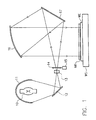
- Fig. 1 is schematically illustrates one example, according to the invention, of an arrangement of an ultraviolet light source for implementing irradiation of the alignment layer on a substrate of a liquid cristal cell.
- a lamp 10 for which the discharge lamp schown in Fig. 2 can be used for direct currents, or a discharge lamp for alternating currents can be used with the same arrangement.
- Lamp 10 is located at a first focal point of an oval focussing mirror 11.
- a first flat reflector 12 reflects light emitting by lamp 10 through an integrator lens 13.
- an integrator lens 13 Directly in front of or behind integrator lens 13, there is a circular diaphragm which is not shown in the drawing. The reason for this is to prevent the visual angle of the light irradiating the workpiece from differing according to the direction on the workpiece surface, because the arc spot of lamp 10 is not actually circular (spherical).
- the shape of the light beam can be determined by the arrangement of the circular diaphragm.
- a collimator 16 is also provided and for which a collimation lens (convex lens) or a collimation mirror (concave mirror) can be used.
- collimator 16 is a collimation mirror (concave mirror).
- an irradiation device can be formed at low cost and it irradiates a larger surface than a lens.
- a second plane mirror 17 enables the degree of freedom of the arrangement of oval focussing mirror 11, collimation mirror 16 or the like to be increased and a compact device obtained.
- a mask MK on which a light screening pattern is formed, and a workpiece WE on which several devices of liquid crystal displays are formed are disposed below collimator 16.
- Mask MK and workpiece WE are, as was described above, spaced at a distance of roughly 100 ⁇ m (microns) from one another, an oxygen-containing gas layer being formed between them.
- Workpiece WE is, furthermore, located on a workpiece carrier WS, such that its alignment layer becomes the upper surface, and is held in place using an attachment means such as, for example, a vacuum chuck or the like.
- Workpiece WE has conventionally four or six devices and has a maximum size of 600 mm x 700 mm; however, conventionally, a size of roughly 365 mm x 460 mm is used.
- ultraviolet light which is emitted from lamp 10 is concentrated by means of oval focussing mirror 11 and is incident via first plane mirror 12 on integrator lens 13. Furthermore, it is incident via shutter 14 and second plane mirror 17 on collimator 16. The ultraviolet light which is reflected from collimator 16 irradiates workpiece WE via mask MK.
- Fig. 2 shows one example of the discharge lamp 1 according to the invention for direct current which emits ultraviolet light.
- Discharge lamp 1 has an arc tube 2 made of quartz glass, within which mercury and rare gas or metallic cadmium and rare gas are encapsulated.
- an amount of mercury M Q (mg/cm 3 (cc)) in the range of 2 ⁇ M Q ⁇ 15 and an encapsulation pressure P1 (Pa) of the rare gas in the range of 0.1 x 10 5 ⁇ P1 ⁇ 5 x 10 5 are selected.
- an amount of cadmium C (mg/cm 3 (cc)) in the range of 0.06 ⁇ C ⁇ 3 is selected together with an encapsulation pressure P2 (Pa) of the rare gas in the range of 0.1 x 10 5 ⁇ P2 ⁇ 3 x 10 6 .
- Electrodes 3 comprise an anode 3a and a cathode 3b.
- the distance between electrodes 3a and 3b is roughly 7.5 mm to 29 mm in order that the arc length is 7.5 mm to 29 mm.
- reference number 4 designates lamp holder end caps. While Fig. 2 shows a discharge lamp for direct current, in the same way, a discharge lamp for alternating current can be provided in which the electrodes have a different shape, but other aspects are essentially the same.
- Fig. 3 is a schematic depiction in which the ultraviolet light source shown in Fig. 1 is described and explained in simplified form.
- the collimation mirror serving as collimator 16 is replaced by a collimation lens (convex lens).
- the collimation mirror (concave mirror) and collimation lens (convex lens) have equivalent functions as a collimator, in which only their optical paths differ from one another with respect to reflection or transmission.
- the magnification factor M S of oval focussing mirror 11 in the range from 10 to 60 is used.
- the angle of incidence of the light incident on integrator lens 13 becomes greater, by which construction of the integrator lens becomes difficult, and by which uniformity is difficult to achieve.
- magnification factor M S of oval focussing mirror 11 If, conversely, the magnification factor is increased, a large integrator lens is needed according to the size of the enlarged arc spot. Furthermore, in this case, deterioration of visual angle ⁇ occurs. It is therefore necessary to select an optimum magnification factor for magnification factor M S of oval focussing mirror 11 according to the applications. In the computation given below, a magnification factor of 18 is used.
- a reduction coefficient K through the diaphragm of roughly 0.65 is conventionally used.
- Distance L between integrator lens 13 and collimator 16 is determined by the required irradiation surface and by divergence angle ⁇ of the light emitted from integrator lens 13.
- divergence angle ⁇ is defined as the half angle of scattering of the light which has emerged from integrator lens 13, as is illustrated in Fig. 3. This means that the larger divergence angle ⁇ , the smaller distance L becomes, the more the light increases and the larger the surface which can be irradiated by means of a compact optical system. If, however, divergence angle ⁇ increases too much, the curvature of collimator 16 becomes greater, by which production becomes difficult, and moreover, the image error (or aberration) becomes greater.
- a divergence angle ⁇ of 5 to 15° is used.
- a large irradiation surface is required, as was described above.
- the visual angle ⁇ of the light incident on mask MK can be ascertained using a feasible optical system in the range from 1.5° ⁇ ⁇ ⁇ 5.7° , by which activation of the undesired areas due to entry of adverse light can be prevented.
- the energy emitted by the lamp can be increased to a sufficient degree in comparison to a conventional discharge lamp of the short arc type by the measure by which the arc length A is the above described length. In this way, irradiation of the alignment layer on a substrate of a liquid crystal cell with the desired duration is enabled.
- an arc power (power which is supplied to the arc for which the loss, as in a voltage drop across the electrodes or the like, was subtracted, and which corresponds to the emission intensity) of roughly 20 to 100 W/mm can be obtained. Therefore, light energy which is necessary for activation, as was described above, can be drawn off by the measure by which the arc length is roughly 7.5 mm to 29 mm.
- Fig. 9 shows the overall configuration of the surface irradiation device according to the invention.
- an ultraviolet irradiation part 20 is identical to the ultraviolet light source which is shown in Fig. 1, and thus, is not further described here.
- the lamp within irradiation part 20 not only a mercury discharge lamp or cadmium lamp, but also an electrodeless arc tube can be used, as is described below.
- the ultraviolet light from this irradiation part 20 is incident on workpiece WE through mask MK.
- the above described alignment layer is formed on workpiece WE.
- Mask MK and workpiece WE are, as was described above, arranged at a distance of roughly 100 ⁇ m (microns) from one another, in which an oxygen-containing gas layer is formed between them.
- workpiece WE is placed on workpiece carrier 25, such that the alignment layer becomes the upper surface, and is attached using a means such as a vacuum chuck or the like.
- workpiece WE is irradiated overall with ultraviolet light, and thus, activation of the alignment layer of each substrate is accomplished.
- any area of workpiece WE to be irradiated can also be exposed in steps and the alignment layer can be activated by gradually moving workpiece WE.
- a base 21 supports the mask carrier 22 which holds mask MK.
- Mask carrier 22 has a positioning device for setting mask MK in a predetermined position and a vacuum chuck for holding the mask by vacuum suction.
- a device 23 is provided for adjusting the mask MK relative to the workpiece WE in directions parallel to one another, and at the same time with a constant distance, is located between the base 21 and the mask carrier 22 at least at three points.
- this distance setting device reference is made to earlier European patent application EP 0 633 505 A1 of the same assignee.
- a device 24 serves for moving the mask carrier 22 to a predetermined position.
- a device 26 serves for moving the workpiece carrier 25 to a predetermined position.
- a microscope 27 has a light source 27a, which emits alignment light, and a CCD sensor 27b. The light from the light source 27a is radiated onto the mask MK and the workpiece WE, the light reflected therefrom is picked up by the CCD sensor 27b, and the alignment marks of mask MK and workpiece WE are brought into agreement with one another.
- a control element 28 which is comprised of a processor or the like, controls the positions of the mask MK and workpiece WE by means of the device 24 for moving the mask carrier and by means of the workpiece carrier 26 which, at the same time, controls distance setting device 23, and which also controls the irradiation part 20.
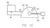
- Fig. 10 shows a light source which emits ultraviolet light, in which, as the lamp which emits the ultraviolet light, a lamp provided with electrodes, such as a mercury discharge lamp or a cadmium lamp, is not used, and in which an electrodeless lamp M1 is used instead.
- a lamp provided with electrodes such as a mercury discharge lamp or a cadmium lamp
- a microwave cavity M2 functions as an oval focussing mirror for the spherical electrodeless lamp M1, and a magnetron M3, which is connected to a current source (not shown in the drawing), feeds microwaves to the cavity M2 via a waveguide M4 and a window M5.
- a motor M6 is provided for turning lamp M1
- a cooling tube M7 is provided for cooling the lamp
- a metal mesh M8 covers the open end of the microwave cavity M2.
- lamp M1 Via the microwave power produced by magnetron M3 and routed by means of waveguide M4 through feed window M5 into the microwave cavity M2, a mixed gas within lamp M1 is excited and ultraviolet light is produced. Furthermore, lamp M1 is turned by motor M6 and cooled by cooling air which is blown in through cooling tube M7.
- electrodeless lamp M1 for example, a lamp with an encapsulated mixed gas can be used as described below:
- the "arc length" in this electrodeless lamp is identical to the inside diameter of the spherical part of the arc tube.
Landscapes
- Physics & Mathematics (AREA)
- General Physics & Mathematics (AREA)
- Health & Medical Sciences (AREA)
- Engineering & Computer Science (AREA)
- Nonlinear Science (AREA)
- Environmental & Geological Engineering (AREA)
- Epidemiology (AREA)
- Public Health (AREA)
- Atmospheric Sciences (AREA)
- Life Sciences & Earth Sciences (AREA)
- Toxicology (AREA)
- Spectroscopy & Molecular Physics (AREA)
- Chemical & Material Sciences (AREA)
- Crystallography & Structural Chemistry (AREA)
- Mathematical Physics (AREA)
- Optics & Photonics (AREA)
- Exposure And Positioning Against Photoresist Photosensitive Materials (AREA)
- Liquid Crystal (AREA)
- Physical Or Chemical Processes And Apparatus (AREA)
Claims (11)
- Procédé d'irradiation d'une surface, comprenant les étapes de mise en place d'un masque et d'une pièce à traiter de manière adjacente l'un à l'autre, formation d'une couche de gaz contenant de l'oxygène entre le masque et la pièce à traiter, irradiation avec une lumière ultraviolette d'une surface de la pièce à traiter à travers le masque selon une direction sensiblement verticale ; dans lequel ladite étape d'irradiation est réalisée avec une lumière ultraviolette parallèle tout en satisfaisant simultanément aux conditions α > 1,5° et d x tan α ≤ 0,1 W, où α est un angle visuel de la lumière ultraviolette, d est une épaisseur de la couche de gaz entre le masque et la pièce à traiter, et W est une largeur d'une unité minimale d'aires de la surface de la pièce à traiter par irradiation.
- Procédé d'irradiation d'une surface selon la revendication 1, dans lequel ladite étape d'irradiation est réalisée en utilisant une source de lumière comprenant une lampe qui émet une lumière qui contient au moins une lumière ultraviolette avec des longueurs d'onde comprises entre 200 nm et 300 nm, un miroir de focalisation ovale qui concentre la lumière émise par la lampe, et un système optique qui contient au moins une lentille intégratrice et un collimateur et, avec le masque, à travers lequel la surface de la pièce à traiter est irradiée, est situé de manière adjacente à la pièce à traiter, au-dessus de la couche de gaz contenant de l'oxygène.
- Procédé d'irradiation d'une surface selon la revendication 1, comprenant les étapes supplémentaires de maintien du masque avec un organe porte-masque et de maintien de la pièce à traiter avec un porte-pièce d'un organe porte-pièce qui possède un dispositif de mouvement pour faire tourner et déplacer le porte-pièce dans des directions horizontales et verticales ; et dans lequel lesdites étapes de mise en place et de formation sont réalisées en utilisant un dispositif de commande pour manoeuvrer lesdits organes de support (porte-masque et porte-pièce) et un dispositif de positionnement pour régler la distance entre la pièce à traiter et le masque.
- Procédé d'irradiation d'une surface selon la revendication 1, dans lequel ladite étape d'irradiation est réalisée en utilisant une lampe à décharge au mercure ayant un tube à arc fait de verre quartzeux dans lequel se trouvent deux électrodes espacées d'une distance produisant une longueur d'arc qui est supérieure ou égale à 7,5 mm et inférieure ou égale à 29 mm, et dans lequel au moins du mercure et un gaz rare sont encapsulés, le mercure étant encapsulé à raison d'une quantité MQ (mg/cm3) qui est comprise dans une plage de 2 ≤ MQ ≤ 15, et le gaz rare étant encapsulé sous une pression P1 (Pa) à température ambiante qui est comprise dans une plage de 0,1 x 10⁵ ≤ P1 ≤ 5 x 10⁵.
- Procédé d'irradiation d'une surface selon la revendication 1, dans lequel ladite étape d'irradiation est réalisée en utilisant une lampe au cadmium ayant un tube à arc fait de verre quartzeux dans lequel se trouvent deux électrodes espacées d'une distance produisant une longueur d'arc qui est supérieure ou égale à 7,5 mm et inférieure ou égale à 29 mm, et dans lequel au moins du cadmium métallique et un gaz rare sont encapsulés, le cadmium étant encapsulé à raison d'une quantité C (mg/cm3) qui est comprise dans une plage de 0,06 ≤ C ≤ 3, et le gaz rare étant encapsulé sous une pression P2 (Pa) à température ambiante qui est comprise dans une plage de 0,1 x 10⁵ ≤ P2 ≤ 3 x 10⁶.
- Procédé d'irradiation d'une surface selon la revendication 1, dans lequel ladite étape d'irradiation est réalisée en utilisant une lampe qui possède un tube à arc sphérique sans électrode, avec un diamètre intérieur qui est supérieur ou égal à 7,5 mm et inférieur ou égal à 29 mm et un miroir de focalisation ovale, une enceinte à cavité hyperfréquence (micro-onde) qui forme une cavité hyperfréquence dans laquelle est situé le tube à arc sans électrode et dans laquelle est réalisé un couplage aux micro-ondes et qui, en même temps, fonctionne comme un miroir de focalisation ovale, un magnétron pour générer des micro-ondes, et des moyens de guide d'ondes et de couplage pour introduire les micro-ondes générées par le magnétron à l'intérieur de la cavité hyperfréquence ; et des moyens de refroidissement pour refroidir le tube à arc sans électrode.
- Dispositif pour mettre en oeuvre le procédé d'irradiation de surface selon la revendication 1, comprenant une source lumineuse pour irradier la pièce à traiter à travers le masque, selon une direction sensiblement verticale, avec une lumière ultraviolette parallèle tout en satisfaisant simultanément aux conditions α > 1,5° et d x tan α ≤ 0,1 W, où α est un angle visuel de la lumière ultraviolette, d est une épaisseur de la couche de gaz entre le masque et la pièce à traiter, et W est une largeur d'une unité minimale d'aires de la surface de la pièce à activer, ledit dispositif comprenant une lampe qui émet une lumière contenant au moins une lumière ultraviolette avec des longueurs d'onde comprises entre 200 nm et 300 nm, un miroir de focalisation ovale qui concentre la lumière émise par la lampe, et un système optique qui contient au moins une lentille intégratrice et un collimateur.
- Dispositif selon la revendication 7, comprenant un organe porte-masque pour maintenir le masque ; un organe porte-pièce ayant un porte-pièce pour maintenir la pièce à traiter, et un dispositif de mouvement pour faire tourner et déplacer le porte-pièce dans des directions horizontales et verticales ; un dispositif de réglage de la distance entre la pièce à traiter et le masque pour former une couche de gaz contenant de l'oxygène entre la pièce à traiter et le masque ; et un élément de commande pour manoeuvrer lesdits organes de support (porte-masque et porte-pièce) et le dispositif de positionnement pour régler la distance de la pièce à traiter par rapport au masque.
- Dispositif selon la revendication 8, comprenant une lampe à décharge au mercure ayant un tube à arc fait de verre quartzeux dans lequel se trouvent deux électrodes espacées d'une distance produisant une longueur d'arc qui est supérieure ou égale à 7,5 mm et inférieure ou égale à 29 mm, et dans lequel au moins du mercure et un gaz rare sont encapsulés, le mercure étant encapsulé à raison d'une quantité MQ (mg/cm3) qui est comprise dans une plage de 2 ≤ MQ ≤ 15, et le gaz rare étant encapsulé sous une pression P1 (Pa) à température ambiante qui est comprise dans une plage de 0,1 x 10⁵ ≤ P1 ≤ 5 x 10⁵.
- Dispositif selon la revendication 8, comprenant une lampe au cadmium ayant un tube à arc fait de verre quartzeux dans lequel se trouvent deux électrodes espacées d'une distance produisant une longueur d'arc qui est supérieure ou égale à 7,5 mm et inférieure ou égale à 29 mm, et dans lequel au moins du cadmium métallique et un gaz rare sont encapsulés, le cadmium étant encapsulé à raison d'une quantité C (mg/cm3) qui est comprise dans une plage de 0,06 ≤ C ≤ 3, et le gaz rare étant encapsulé sous une pression P2 (Pa) à température ambiante qui est comprise dans une plage de 0,1 x 10⁵ ≤ P2 ≤ 3 x 10⁶.
- Dispositif selon la revendication 8, comprenant une lampe qui émet une lumière ultraviolette ayant un tube à arc sphérique sans électrode, avec un diamètre intérieur qui est supérieur ou égal à 7,5 mm et inférieur ou égal à 29 mm et un miroir de focalisation ovale ; une enceinte à cavité hyperfréquence (micro-onde) qui forme une cavité hyperfréquence dans laquelle est situé le tube à arc sans électrode et dans laquelle est réalisé un couplage aux micro-ondes et qui, en même temps, fonctionne comme un miroir de focalisation ovale ; un magnétron pour générer des micro-ondes ; un guide d'ondes pour introduire les micro-ondes générées par le magnétron dans la cavité hyperfréquence ; des moyens de couplage pour coupler les micro-ondes introduites par le guide d'ondes dans la cavité hyperfréquence ; et des moyens de refroidissement pour refroidir le tube à arc sans électrode.
Applications Claiming Priority (6)
| Application Number | Priority Date | Filing Date | Title |
|---|---|---|---|
| JP17528295 | 1995-07-11 | ||
| JP17528195 | 1995-07-11 | ||
| JP17528295 | 1995-07-11 | ||
| JP175281/95 | 1995-07-11 | ||
| JP17528195 | 1995-07-11 | ||
| JP175282/95 | 1995-07-11 |
Publications (3)
| Publication Number | Publication Date |
|---|---|
| EP0754976A2 EP0754976A2 (fr) | 1997-01-22 |
| EP0754976A3 EP0754976A3 (fr) | 1999-06-02 |
| EP0754976B1 true EP0754976B1 (fr) | 2003-06-04 |
Family
ID=26496599
Family Applications (1)
| Application Number | Title | Priority Date | Filing Date |
|---|---|---|---|
| EP96111119A Expired - Lifetime EP0754976B1 (fr) | 1995-07-11 | 1996-07-10 | Procédé pour l'activiation d'une surface ainsi que appareil et lampe pour exécuter ce procédé |
Country Status (5)
| Country | Link |
|---|---|
| US (1) | US5864388A (fr) |
| EP (1) | EP0754976B1 (fr) |
| KR (1) | KR100379873B1 (fr) |
| DE (1) | DE69628504T2 (fr) |
| TW (1) | TW444876U (fr) |
Families Citing this family (18)
| Publication number | Priority date | Publication date | Assignee | Title |
|---|---|---|---|---|
| US6400442B1 (en) * | 1996-08-28 | 2002-06-04 | Polaroid Corporation | Optical system for use in a photographic printer |
| JP4201862B2 (ja) * | 1997-02-27 | 2008-12-24 | シャープ株式会社 | 液晶表示装置 |
| TW536644B (en) * | 1997-10-29 | 2003-06-11 | Ushio Electric Inc | Polarized light radiation device for alignment film of liquid crystal display element |
| JP4238390B2 (ja) * | 1998-02-27 | 2009-03-18 | 株式会社ニコン | 照明装置、該照明装置を備えた露光装置および該露光装置を用いて半導体デバイスを製造する方法 |
| US6833904B1 (en) | 1998-02-27 | 2004-12-21 | Nikon Corporation | Exposure apparatus and method of fabricating a micro-device using the exposure apparatus |
| JP3517583B2 (ja) | 1998-03-27 | 2004-04-12 | キヤノン株式会社 | 露光装置、デバイス製造方法及び放電灯 |
| JP2000123786A (ja) * | 1998-10-13 | 2000-04-28 | Matsushita Electronics Industry Corp | 高圧水銀ランプ、この高圧水銀ランプを用いた照明光学装置、およびこの照明光学装置を用いた画像表示装置 |
| US6532047B1 (en) | 1998-10-27 | 2003-03-11 | Ushiodenki Kabushiki Kaisha | Irradiation device for polarized light for optical alignment of a liquid crystal cell element |
| JP3458733B2 (ja) * | 1998-11-24 | 2003-10-20 | ウシオ電機株式会社 | 斜め光照射装置 |
| US6492772B1 (en) * | 1999-02-10 | 2002-12-10 | Matsushita Electric Industrial Co., Ltd. | High pressure discharge lamp, high pressure discharge lamp electrode, method of producing the high pressure discharge lamp electrode, and illumination device and image display apparatus respectively using the high pressure discharge lamps |
| JP2002189301A (ja) * | 2000-12-22 | 2002-07-05 | Ushio Inc | 光配向用偏光光照射装置 |
| US6908586B2 (en) * | 2001-06-27 | 2005-06-21 | Fusion Uv Systems, Inc. | Free radical polymerization method having reduced premature termination, apparatus for performing the method and product formed thereby |
| US20030104171A1 (en) * | 2001-11-29 | 2003-06-05 | Maclachlan Julia | Method of using short wavelength UV light to selectively remove a coating from a substrate and article produced thereby |
| JP2007290233A (ja) * | 2006-04-25 | 2007-11-08 | Ushio Inc | 光照射器およびインクジェットプリンタ |
| JP2010087388A (ja) * | 2008-10-02 | 2010-04-15 | Ushio Inc | 露光装置 |
| TWI404922B (zh) * | 2010-02-02 | 2013-08-11 | Chroma Ate Inc | Spectral spectral measurement system |
| JP5688730B2 (ja) * | 2010-09-17 | 2015-03-25 | 株式会社ブイ・テクノロジー | 露光装置 |
| CN107561871B (zh) * | 2016-07-01 | 2020-04-10 | 上海微电子装备(集团)股份有限公司 | 接近式曝光和光配向一体装置、光配向方法及曝光方法 |
Family Cites Families (12)
| Publication number | Priority date | Publication date | Assignee | Title |
|---|---|---|---|---|
| DE2116713B2 (de) * | 1971-04-06 | 1974-03-28 | Ibm Deutschland Gmbh, 7000 Stuttgart | Belichtungsverfahren zum Abbilden sehr fein strukturierter Lichtmuster auf Photolackschichten und dazu geeignete Belichtungsvorrichtung |
| US4023904A (en) * | 1974-07-01 | 1977-05-17 | Tamarack Scientific Co. Inc. | Optical microcircuit printing process |
| US4485332A (en) * | 1982-05-24 | 1984-11-27 | Fusion Systems Corporation | Method & apparatus for cooling electrodeless lamps |
| US4859906A (en) * | 1982-10-06 | 1989-08-22 | Fusion Systems Corportion | Deep UV lamp bulb with improved fill |
| NL184550C (nl) * | 1982-12-01 | 1989-08-16 | Philips Nv | Gasontladingslamp. |
| NL191812C (nl) * | 1987-09-04 | 1996-08-02 | Philips Electronics Nv | Hogedrukgasontladingslamp en armatuur voorzien van die lamp. |
| US4975625A (en) * | 1988-06-24 | 1990-12-04 | Fusion Systems Corporation | Electrodeless lamp which couples to small bulb |
| US5673102A (en) * | 1991-02-22 | 1997-09-30 | Canon Kabushiki Kaisha | Image farming and microdevice manufacturing method and exposure apparatus in which a light source includes four quadrants of predetermined intensity |
| JP3291818B2 (ja) * | 1993-03-16 | 2002-06-17 | 株式会社ニコン | 投影露光装置、及び該装置を用いる半導体集積回路製造方法 |
| JP2775694B2 (ja) * | 1993-05-07 | 1998-07-16 | ウシオ電機株式会社 | 放電ランプ |
| KR100208739B1 (ko) * | 1993-07-08 | 1999-07-15 | 다나카 아키히로 | 작업편과 마스크의 간극설정방법 및 간극설정기구 |
| TW259845B (fr) * | 1993-07-30 | 1995-10-11 | Sharp Kk |
-
1996
- 1996-06-27 KR KR1019960024752A patent/KR100379873B1/ko not_active Expired - Lifetime
- 1996-07-10 EP EP96111119A patent/EP0754976B1/fr not_active Expired - Lifetime
- 1996-07-10 DE DE69628504T patent/DE69628504T2/de not_active Expired - Lifetime
- 1996-07-11 US US08/680,317 patent/US5864388A/en not_active Expired - Lifetime
- 1996-07-11 TW TW087220583U patent/TW444876U/zh not_active IP Right Cessation
Also Published As
| Publication number | Publication date |
|---|---|
| DE69628504D1 (de) | 2003-07-10 |
| US5864388A (en) | 1999-01-26 |
| EP0754976A3 (fr) | 1999-06-02 |
| TW444876U (en) | 2001-07-01 |
| EP0754976A2 (fr) | 1997-01-22 |
| KR100379873B1 (ko) | 2003-08-21 |
| DE69628504T2 (de) | 2004-04-29 |
| KR970007443A (ko) | 1997-02-21 |
Similar Documents
| Publication | Publication Date | Title |
|---|---|---|
| US5864388A (en) | Surface activating process, and device and lamp for performing said process | |
| US5207505A (en) | Illumination light source device | |
| EP2172962B1 (fr) | Dispositif d'exposition | |
| EP2534672B1 (fr) | Source lumineuse commandée par laser | |
| US7705331B1 (en) | Methods and systems for providing illumination of a specimen for a process performed on the specimen | |
| US7786455B2 (en) | Laser-driven light source | |
| US4532427A (en) | Method and apparatus for performing deep UV photolithography | |
| US20100164380A1 (en) | Light source | |
| US5144190A (en) | Light source having desired color temperature and chromaticity | |
| EP1717638B1 (fr) | Appareil d'exposition aux rayonnements UV extrêmes et source de rayonnements UV extrêmes | |
| JP3827492B2 (ja) | 放電灯 | |
| JP2004361746A (ja) | 露光用照明装置 | |
| US5059146A (en) | Method of adjusting a light source for color temperature and chromaticity | |
| KR20040090481A (ko) | 광원장치 및 화상표시장치 | |
| US5681394A (en) | Photo-excited processing apparatus and method for manufacturing a semiconductor device by using the same | |
| US3727525A (en) | Device for making phosphor screen for color picture tubes | |
| US6850367B2 (en) | Light exposure apparatus and light emitting device therefor | |
| US5670844A (en) | Discharge lamp | |
| TWI343588B (en) | Increasing the discharge arc diffuseness in mercury-free gas discharge lamps | |
| JP2002237442A (ja) | 照度分布均一化フィルタを備えた光照射装置 | |
| JPH09210911A (ja) | 光安定性試験装置 | |
| US5368647A (en) | Photo-excited processing apparatus for manufacturing a semiconductor device that uses a cylindrical reflecting surface | |
| JP3204100B2 (ja) | 膜質改質方法および膜質改質用光源 | |
| JP3149791B2 (ja) | 膜質改質装置 | |
| TWI410754B (zh) | 用於遮蔽弧燈之一部份之蓋、弧燈、及微影裝置 |
Legal Events
| Date | Code | Title | Description |
|---|---|---|---|
| PUAI | Public reference made under article 153(3) epc to a published international application that has entered the european phase |
Free format text: ORIGINAL CODE: 0009012 |
|
| AK | Designated contracting states |
Kind code of ref document: A2 Designated state(s): DE GB NL |
|
| PUAL | Search report despatched |
Free format text: ORIGINAL CODE: 0009013 |
|
| AK | Designated contracting states |
Kind code of ref document: A3 Designated state(s): DE GB NL |
|
| 17P | Request for examination filed |
Effective date: 19991117 |
|
| 17Q | First examination report despatched |
Effective date: 20010720 |
|
| GRAH | Despatch of communication of intention to grant a patent |
Free format text: ORIGINAL CODE: EPIDOS IGRA |
|
| GRAH | Despatch of communication of intention to grant a patent |
Free format text: ORIGINAL CODE: EPIDOS IGRA |
|
| GRAA | (expected) grant |
Free format text: ORIGINAL CODE: 0009210 |
|
| AK | Designated contracting states |
Designated state(s): DE GB NL |
|
| REG | Reference to a national code |
Ref country code: GB Ref legal event code: FG4D |
|
| REF | Corresponds to: |
Ref document number: 69628504 Country of ref document: DE Date of ref document: 20030710 Kind code of ref document: P |
|
| PLBE | No opposition filed within time limit |
Free format text: ORIGINAL CODE: 0009261 |
|
| STAA | Information on the status of an ep patent application or granted ep patent |
Free format text: STATUS: NO OPPOSITION FILED WITHIN TIME LIMIT |
|
| 26N | No opposition filed |
Effective date: 20040305 |
|
| PGFP | Annual fee paid to national office [announced via postgrant information from national office to epo] |
Ref country code: GB Payment date: 20120704 Year of fee payment: 17 |
|
| PGFP | Annual fee paid to national office [announced via postgrant information from national office to epo] |
Ref country code: DE Payment date: 20120704 Year of fee payment: 17 |
|
| PGFP | Annual fee paid to national office [announced via postgrant information from national office to epo] |
Ref country code: NL Payment date: 20120714 Year of fee payment: 17 |
|
| REG | Reference to a national code |
Ref country code: NL Ref legal event code: V1 Effective date: 20140201 |
|
| GBPC | Gb: european patent ceased through non-payment of renewal fee |
Effective date: 20130710 |
|
| PG25 | Lapsed in a contracting state [announced via postgrant information from national office to epo] |
Ref country code: DE Free format text: LAPSE BECAUSE OF NON-PAYMENT OF DUE FEES Effective date: 20140201 Ref country code: NL Free format text: LAPSE BECAUSE OF NON-PAYMENT OF DUE FEES Effective date: 20140201 Ref country code: GB Free format text: LAPSE BECAUSE OF NON-PAYMENT OF DUE FEES Effective date: 20130710 |
|
| REG | Reference to a national code |
Ref country code: DE Ref legal event code: R119 Ref document number: 69628504 Country of ref document: DE Effective date: 20140201 |