EP0756331B1 - Composant limiteur de courant et procédé de réalisation - Google Patents
Composant limiteur de courant et procédé de réalisation Download PDFInfo
- Publication number
- EP0756331B1 EP0756331B1 EP96420258A EP96420258A EP0756331B1 EP 0756331 B1 EP0756331 B1 EP 0756331B1 EP 96420258 A EP96420258 A EP 96420258A EP 96420258 A EP96420258 A EP 96420258A EP 0756331 B1 EP0756331 B1 EP 0756331B1
- Authority
- EP
- European Patent Office
- Prior art keywords
- microns
- zone
- current
- doped
- component
- Prior art date
- Legal status (The legal status is an assumption and is not a legal conclusion. Google has not performed a legal analysis and makes no representation as to the accuracy of the status listed.)
- Expired - Lifetime
Links
Images
Classifications
-
- H—ELECTRICITY
- H10—SEMICONDUCTOR DEVICES; ELECTRIC SOLID-STATE DEVICES NOT OTHERWISE PROVIDED FOR
- H10D—INORGANIC ELECTRIC SEMICONDUCTOR DEVICES
- H10D8/00—Diodes
- H10D8/80—PNPN diodes, e.g. Shockley diodes or break-over diodes
Definitions
- the present invention relates to a component limiting current, therefore intended to be connected in series on the branch of circuit for which a current limitation is desired.
- the invention which aims to remedy these drawbacks of these known components, proposes a component limiting overcurrent which is able to withstand a nominal current of several dozen Amps, and which reacts very quickly to an accidental overcurrent, its reaction time being by example of the order of a microsecond.
- the respective doping characteristics of these four successive zones N, P, N, P are such that, for low current levels, the sum of the gains in PNP bipolar transistor current formed by the three first zones and of the NPN bipolar transistor formed by the last three zones is equal to 1.
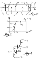
- the limiter component of invention 1 is shown connected in series on a line electric 2 which is traversed by an electric current unidirectional whose nominal intensity IN is for example of 50 Amps.
- This component 1 is provided with two electrodes, an anode 3 and a cathode 4, which conventionally allow it to be connected in series on power line 2.
- characteristic I (V) is that of a diode supplied with direct, or C1
- the voltage drop V across the component therefore remaining very weak as is the case for a diode polarized live.
- the operating point N has been marked on the curve nominal, for which the current I is the nominal current IN, by example 5 Amperes, while the voltage drop VN aux component terminals is less than 1 Volt.
- the level C2 is due to a phenomenon of desaturation already mentioned for some authors. This phenomenon is, in the thyristor domain, a parasitic phenomenon, and the latter are therefore carried out so as to avoid it, unlike the invention where this phenomenon is, well at otherwise, advantageously exploited.
- FIG. 3 An equivalent diagram of component 1 is shown on FIG. 3, where the layers 5, 6, 7 define a transistor 13 of PNP type, while layers 6,7,8 define another transistor 14, of NPN type.
- This equivalent scheme is not only approximate, since component 1 does not hold the voltage reverse, which would not necessarily be the case for a circuit arranged according to Figure 3.
- the manufacturing technology of this current limiter 1 can be either a "planar” technology or a technology “mesa”.
- the lifespan of the carriers This duration life is not constant in structure and it is possible that the component works for a duration distribution of life and it doesn't work for another distribution (this distribution depending in particular on manufacturing conditions).
Landscapes
- Bipolar Integrated Circuits (AREA)
- Thyristors (AREA)
- Bipolar Transistors (AREA)
- Emergency Protection Circuit Devices (AREA)
- Tone Control, Compression And Expansion, Limiting Amplitude (AREA)
Applications Claiming Priority (2)
| Application Number | Priority Date | Filing Date | Title |
|---|---|---|---|
| FR9509442A FR2737343B1 (fr) | 1995-07-28 | 1995-07-28 | Composant limiteur de courant et procede de realisation |
| FR9509442 | 1995-07-28 |
Publications (2)
| Publication Number | Publication Date |
|---|---|
| EP0756331A1 EP0756331A1 (fr) | 1997-01-29 |
| EP0756331B1 true EP0756331B1 (fr) | 1999-12-15 |
Family
ID=9481668
Family Applications (1)
| Application Number | Title | Priority Date | Filing Date |
|---|---|---|---|
| EP96420258A Expired - Lifetime EP0756331B1 (fr) | 1995-07-28 | 1996-07-26 | Composant limiteur de courant et procédé de réalisation |
Country Status (7)
| Country | Link |
|---|---|
| US (1) | US5696390A (da) |
| EP (1) | EP0756331B1 (da) |
| DE (1) | DE69605615T2 (da) |
| DK (1) | DK0756331T3 (da) |
| ES (1) | ES2140049T3 (da) |
| FR (1) | FR2737343B1 (da) |
| PT (1) | PT756331E (da) |
Families Citing this family (3)
| Publication number | Priority date | Publication date | Assignee | Title |
|---|---|---|---|---|
| FR2789519B1 (fr) * | 1999-02-05 | 2003-03-28 | Commissariat Energie Atomique | Transistor mos a tension de seuil dynamique equipe d'un limiteur de courant, et procede de realisation d'un tel transistor |
| US6674129B1 (en) * | 1999-12-17 | 2004-01-06 | Koninklijke Phillips Electronics N.V. | ESD diode structure |
| US6501630B1 (en) | 1999-12-17 | 2002-12-31 | Koninklijke Philips Electronics N.V. | Bi-directional ESD diode structure |
Family Cites Families (11)
| Publication number | Priority date | Publication date | Assignee | Title |
|---|---|---|---|---|
| NL239104A (da) * | 1958-05-26 | 1900-01-01 | Western Electric Co | |
| NL251532A (da) * | 1959-06-17 | |||
| US3175934A (en) * | 1960-01-19 | 1965-03-30 | Hitachi Ltd | Semiconductor switching element and process for producing the same |
| US3093755A (en) * | 1960-07-07 | 1963-06-11 | Mallory & Co Inc P R | Semiconductor diode exhibiting differential negative resistance |
| NL266849A (da) * | 1960-07-19 | |||
| DE1614440A1 (de) * | 1967-03-08 | 1970-07-16 | Siemens Ag | Thyristor |
| FR2458905A1 (fr) * | 1979-06-06 | 1981-01-02 | Silicium Semiconducteur Ssc | Diode de shockley et son procede de fabrication |
| JPH0638508B2 (ja) * | 1988-05-12 | 1994-05-18 | 工業技術院長 | 半導体サージ保護素子 |
| DE58909264D1 (de) * | 1988-06-21 | 1995-07-06 | Siemens Ag | Diode mit verbessertem Abschaltverhalten. |
| DE3931589A1 (de) * | 1989-09-22 | 1991-04-04 | Bosch Gmbh Robert | Halbleiterschaltelement |
| US5483086A (en) * | 1993-04-20 | 1996-01-09 | Shindengen Electric Manufacturing Co., Ltd. | Four layer semiconductor surge protector having plural short-circuited junctions |
-
1995
- 1995-07-28 FR FR9509442A patent/FR2737343B1/fr not_active Expired - Fee Related
-
1996
- 1996-07-26 ES ES96420258T patent/ES2140049T3/es not_active Expired - Lifetime
- 1996-07-26 PT PT96420258T patent/PT756331E/pt unknown
- 1996-07-26 DK DK96420258T patent/DK0756331T3/da active
- 1996-07-26 EP EP96420258A patent/EP0756331B1/fr not_active Expired - Lifetime
- 1996-07-26 DE DE69605615T patent/DE69605615T2/de not_active Expired - Fee Related
- 1996-07-29 US US08/688,156 patent/US5696390A/en not_active Expired - Fee Related
Also Published As
| Publication number | Publication date |
|---|---|
| DE69605615T2 (de) | 2000-05-31 |
| PT756331E (pt) | 2000-06-30 |
| DE69605615D1 (de) | 2000-01-20 |
| US5696390A (en) | 1997-12-09 |
| DK0756331T3 (da) | 2000-05-01 |
| EP0756331A1 (fr) | 1997-01-29 |
| FR2737343A1 (fr) | 1997-01-31 |
| ES2140049T3 (es) | 2000-02-16 |
| FR2737343B1 (fr) | 1997-10-24 |
Similar Documents
| Publication | Publication Date | Title |
|---|---|---|
| FR2744836A1 (fr) | Substrat epitaxial a concentration progressive pour dispositif a semi-conducteurs a diffusion par resurf | |
| FR2494499A1 (fr) | Structure plane pour dispositifs semi-conducteurs a haute tension | |
| FR2569495A1 (fr) | Procede pour la fabrication de dispositifs a semi-conducteur comportant des jonctions planaires a concentration de charge variable et a tres haute tension de rupture | |
| EP0006474A1 (fr) | Procédé de correction du coefficient en tension de résistances semi-conductrices diffusées ou implantées | |
| EP0368768B1 (fr) | Procédé de fabrication d'une diode rapide et diode rapide obtenue par ce procédé | |
| EP0614232B1 (fr) | Diode de référence dans un circuit intégré bipolaire | |
| SE511816C2 (sv) | Resistor innefattande en resistorkropp av polykristallint kisel samt förfarande för framställning av en sådan | |
| FR2477777A1 (fr) | Transistor bipolaire de puissance | |
| FR2468208A1 (fr) | Dispositif semiconducteur avec une diode zener | |
| EP0624943B1 (fr) | Composant limiteur de courant série | |
| FR3011124A1 (fr) | Composant scr a caracteristiques stables en temperature | |
| EP0756331A1 (fr) | Composant limiteur de courant et procédé de réalisation | |
| EP0002087B1 (fr) | Dispositif semiconducteur monolithique comprenant deux transistors complémentaires et son procédé de fabrication | |
| FR2554276A1 (fr) | Diode de reference pour circuit integre et son procede de fabrication | |
| EP0015835B1 (fr) | Dispositif semiconducteur de commutation à fréquence élevée et procédé pour sa fabrication | |
| EP0110777A1 (fr) | Structure de thyristor à allumage intrinsèque et son application à la réalisation d'un dispositif bidirectionnel | |
| EP0193462B1 (fr) | Diode hyperfréquence de type PIN à transitions abruptes | |
| FR2556882A1 (fr) | Composant semiconducteur rapide, notamment diode pin haute tension | |
| FR2581796A1 (fr) | Circuit integre bipolaire comprenant des transistors pnp verticaux avec collecteur sur le substrat, et procede pour la realisation d'un tel circuit | |
| FR2640813A1 (fr) | Circuit integre presentant un transistor vertical | |
| US3440497A (en) | Semiconductor negative resistance electroluminescent diode | |
| EP0021899A1 (fr) | Diode de Shockley et son procédé de fabrication | |
| FR2570545A1 (fr) | Dispositif a semi-conducteur a resistance enterree | |
| FR2531573A1 (fr) | Transistor integre contre les surtensions | |
| EP0032069A1 (fr) | Procédé d'ajustement du coefficient de température d'une diode de référence et diode de référence obtenue |
Legal Events
| Date | Code | Title | Description |
|---|---|---|---|
| PUAI | Public reference made under article 153(3) epc to a published international application that has entered the european phase |
Free format text: ORIGINAL CODE: 0009012 |
|
| AK | Designated contracting states |
Kind code of ref document: A1 Designated state(s): BE CH DE DK ES FR GB IT LI NL PT SE |
|
| 17P | Request for examination filed |
Effective date: 19970326 |
|
| 17Q | First examination report despatched |
Effective date: 19981103 |
|
| GRAG | Despatch of communication of intention to grant |
Free format text: ORIGINAL CODE: EPIDOS AGRA |
|
| GRAG | Despatch of communication of intention to grant |
Free format text: ORIGINAL CODE: EPIDOS AGRA |
|
| GRAH | Despatch of communication of intention to grant a patent |
Free format text: ORIGINAL CODE: EPIDOS IGRA |
|
| GRAH | Despatch of communication of intention to grant a patent |
Free format text: ORIGINAL CODE: EPIDOS IGRA |
|
| GRAA | (expected) grant |
Free format text: ORIGINAL CODE: 0009210 |
|
| AK | Designated contracting states |
Kind code of ref document: B1 Designated state(s): BE CH DE DK ES FR GB IT LI NL PT SE |
|
| REG | Reference to a national code |
Ref country code: CH Ref legal event code: EP |
|
| GBT | Gb: translation of ep patent filed (gb section 77(6)(a)/1977) |
Effective date: 19991216 |
|
| REF | Corresponds to: |
Ref document number: 69605615 Country of ref document: DE Date of ref document: 20000120 |
|
| REG | Reference to a national code |
Ref country code: ES Ref legal event code: FG2A Ref document number: 2140049 Country of ref document: ES Kind code of ref document: T3 |
|
| ITF | It: translation for a ep patent filed | ||
| REG | Reference to a national code |
Ref country code: DK Ref legal event code: T3 |
|
| REG | Reference to a national code |
Ref country code: PT Ref legal event code: SC4A Free format text: AVAILABILITY OF NATIONAL TRANSLATION Effective date: 20000314 |
|
| PLBE | No opposition filed within time limit |
Free format text: ORIGINAL CODE: 0009261 |
|
| STAA | Information on the status of an ep patent application or granted ep patent |
Free format text: STATUS: NO OPPOSITION FILED WITHIN TIME LIMIT |
|
| 26N | No opposition filed | ||
| PGFP | Annual fee paid to national office [announced via postgrant information from national office to epo] |
Ref country code: SE Payment date: 20010718 Year of fee payment: 6 |
|
| PGFP | Annual fee paid to national office [announced via postgrant information from national office to epo] |
Ref country code: NL Payment date: 20010719 Year of fee payment: 6 Ref country code: DK Payment date: 20010719 Year of fee payment: 6 |
|
| PGFP | Annual fee paid to national office [announced via postgrant information from national office to epo] |
Ref country code: PT Payment date: 20010810 Year of fee payment: 6 |
|
| PGFP | Annual fee paid to national office [announced via postgrant information from national office to epo] |
Ref country code: CH Payment date: 20010814 Year of fee payment: 6 |
|
| PGFP | Annual fee paid to national office [announced via postgrant information from national office to epo] |
Ref country code: BE Payment date: 20010907 Year of fee payment: 6 |
|
| REG | Reference to a national code |
Ref country code: GB Ref legal event code: IF02 |
|
| PG25 | Lapsed in a contracting state [announced via postgrant information from national office to epo] |
Ref country code: SE Free format text: LAPSE BECAUSE OF NON-PAYMENT OF DUE FEES Effective date: 20020727 |
|
| PG25 | Lapsed in a contracting state [announced via postgrant information from national office to epo] |
Ref country code: LI Free format text: LAPSE BECAUSE OF NON-PAYMENT OF DUE FEES Effective date: 20020731 Ref country code: DK Free format text: LAPSE BECAUSE OF NON-PAYMENT OF DUE FEES Effective date: 20020731 Ref country code: CH Free format text: LAPSE BECAUSE OF NON-PAYMENT OF DUE FEES Effective date: 20020731 Ref country code: BE Free format text: LAPSE BECAUSE OF NON-PAYMENT OF DUE FEES Effective date: 20020731 |
|
| BERE | Be: lapsed |
Owner name: CENTRO NACIONAL DE MICROELECTRONICA - *CSIC Effective date: 20020731 Owner name: S.A. *FERRAZ Effective date: 20020731 |
|
| PG25 | Lapsed in a contracting state [announced via postgrant information from national office to epo] |
Ref country code: PT Free format text: LAPSE BECAUSE OF NON-PAYMENT OF DUE FEES Effective date: 20030131 |
|
| PG25 | Lapsed in a contracting state [announced via postgrant information from national office to epo] |
Ref country code: NL Free format text: LAPSE BECAUSE OF NON-PAYMENT OF DUE FEES Effective date: 20030201 |
|
| REG | Reference to a national code |
Ref country code: DK Ref legal event code: EBP |
|
| EUG | Se: european patent has lapsed | ||
| REG | Reference to a national code |
Ref country code: CH Ref legal event code: PL |
|
| NLV4 | Nl: lapsed or anulled due to non-payment of the annual fee |
Effective date: 20030201 |
|
| REG | Reference to a national code |
Ref country code: PT Ref legal event code: MM4A Free format text: LAPSE DUE TO NON-PAYMENT OF FEES Effective date: 20030131 |
|
| PGFP | Annual fee paid to national office [announced via postgrant information from national office to epo] |
Ref country code: ES Payment date: 20080722 Year of fee payment: 13 Ref country code: DE Payment date: 20080715 Year of fee payment: 13 |
|
| PGFP | Annual fee paid to national office [announced via postgrant information from national office to epo] |
Ref country code: IT Payment date: 20080726 Year of fee payment: 13 Ref country code: FR Payment date: 20080710 Year of fee payment: 13 |
|
| PGFP | Annual fee paid to national office [announced via postgrant information from national office to epo] |
Ref country code: GB Payment date: 20080722 Year of fee payment: 13 |
|
| GBPC | Gb: european patent ceased through non-payment of renewal fee |
Effective date: 20090726 |
|
| REG | Reference to a national code |
Ref country code: FR Ref legal event code: ST Effective date: 20100331 |
|
| PG25 | Lapsed in a contracting state [announced via postgrant information from national office to epo] |
Ref country code: FR Free format text: LAPSE BECAUSE OF NON-PAYMENT OF DUE FEES Effective date: 20090731 |
|
| PG25 | Lapsed in a contracting state [announced via postgrant information from national office to epo] |
Ref country code: GB Free format text: LAPSE BECAUSE OF NON-PAYMENT OF DUE FEES Effective date: 20090726 |
|
| PG25 | Lapsed in a contracting state [announced via postgrant information from national office to epo] |
Ref country code: DE Free format text: LAPSE BECAUSE OF NON-PAYMENT OF DUE FEES Effective date: 20100202 |
|
| REG | Reference to a national code |
Ref country code: ES Ref legal event code: FD2A Effective date: 20090727 |
|
| PG25 | Lapsed in a contracting state [announced via postgrant information from national office to epo] |
Ref country code: ES Free format text: LAPSE BECAUSE OF NON-PAYMENT OF DUE FEES Effective date: 20090727 |
|
| PG25 | Lapsed in a contracting state [announced via postgrant information from national office to epo] |
Ref country code: IT Free format text: LAPSE BECAUSE OF NON-PAYMENT OF DUE FEES Effective date: 20090726 |