EP0757443A1 - Circuit pour la dissipation contrÔlé et indépendante d'énergie accumulée inductive des charges inductives multiples - Google Patents
Circuit pour la dissipation contrÔlé et indépendante d'énergie accumulée inductive des charges inductives multiples Download PDFInfo
- Publication number
- EP0757443A1 EP0757443A1 EP95830344A EP95830344A EP0757443A1 EP 0757443 A1 EP0757443 A1 EP 0757443A1 EP 95830344 A EP95830344 A EP 95830344A EP 95830344 A EP95830344 A EP 95830344A EP 0757443 A1 EP0757443 A1 EP 0757443A1
- Authority
- EP
- European Patent Office
- Prior art keywords
- circuit
- node
- load
- active element
- current
- Prior art date
- Legal status (The legal status is an assumption and is not a legal conclusion. Google has not performed a legal analysis and makes no representation as to the accuracy of the status listed.)
- Granted
Links
- 230000001939 inductive effect Effects 0.000 title claims abstract description 65
- 238000004064 recycling Methods 0.000 claims description 56
- 230000000903 blocking effect Effects 0.000 claims description 20
- 238000007599 discharging Methods 0.000 abstract description 6
- 230000001105 regulatory effect Effects 0.000 description 10
- 238000013461 design Methods 0.000 description 5
- 238000010586 diagram Methods 0.000 description 5
- 239000000446 fuel Substances 0.000 description 4
- 230000001276 controlling effect Effects 0.000 description 3
- 230000001419 dependent effect Effects 0.000 description 3
- 238000004519 manufacturing process Methods 0.000 description 3
- 238000000034 method Methods 0.000 description 3
- 230000008569 process Effects 0.000 description 3
- 239000000243 solution Substances 0.000 description 3
- 230000015556 catabolic process Effects 0.000 description 2
- 238000005520 cutting process Methods 0.000 description 2
- 230000006872 improvement Effects 0.000 description 2
- 239000002904 solvent Substances 0.000 description 2
- 230000009471 action Effects 0.000 description 1
- 239000012190 activator Substances 0.000 description 1
- 238000013459 approach Methods 0.000 description 1
- 238000010276 construction Methods 0.000 description 1
- 238000005516 engineering process Methods 0.000 description 1
- 238000002347 injection Methods 0.000 description 1
- 239000007924 injection Substances 0.000 description 1
- 230000010354 integration Effects 0.000 description 1
- 230000000670 limiting effect Effects 0.000 description 1
- 238000012986 modification Methods 0.000 description 1
- 230000004048 modification Effects 0.000 description 1
- 230000003071 parasitic effect Effects 0.000 description 1
- 239000004065 semiconductor Substances 0.000 description 1
- 238000004513 sizing Methods 0.000 description 1
- 238000012546 transfer Methods 0.000 description 1
Images


Classifications
-
- H—ELECTRICITY
- H03—ELECTRONIC CIRCUITRY
- H03K—PULSE TECHNIQUE
- H03K17/00—Electronic switching or gating, i.e. not by contact-making and –breaking
- H03K17/08—Modifications for protecting switching circuit against overcurrent or overvoltage
- H03K17/082—Modifications for protecting switching circuit against overcurrent or overvoltage by feedback from the output to the control circuit
- H03K17/0822—Modifications for protecting switching circuit against overcurrent or overvoltage by feedback from the output to the control circuit in field-effect transistor switches
-
- H—ELECTRICITY
- H03—ELECTRONIC CIRCUITRY
- H03K—PULSE TECHNIQUE
- H03K17/00—Electronic switching or gating, i.e. not by contact-making and –breaking
- H03K17/51—Electronic switching or gating, i.e. not by contact-making and –breaking characterised by the components used
- H03K17/74—Electronic switching or gating, i.e. not by contact-making and –breaking characterised by the components used by the use, as active elements, of diodes
Definitions
- This invention relates to a circuit for controllably and independently recycling the discharge current of a plurality of inductive loads connected between first and second power supply terminals.
- the circuit is of a type which includes, for each of the loads:
- inductive loads As is known, a number of electronic and electromagnetic devices, arranged to perform a variety of functions in motor cars, include one or more inductive loads. Such devices also distinguish themselves by the current that their respective loads are to withstand. Some inductive loads are of relatively small size and can only withstand moderately large currents during their operation. Devices of this kind may include relays of several different types, for example. On the other hand, there are inductive loads of larger size, such as those contained in fuel injection control devices, which can store larger amounts of energy.
- each inductive load has usually one terminal which is kept at a fixed voltage and another terminal connected to a preferably integrated control circuit driving the flow of current through the load.
- the control circuit comprises an active element, such as a driving transistor, which in most cases is a power transistor and performs switching functions to alternately force and interrupt the flow of current through the inductor.
- the active element is controlled by a drive signal generated within the circuit itself.
- the voltage peak should have limited width, for otherwise the peak could cause breakdowns in the junctions of the semiconductor elements present in the control circuit, or in other devices connected to this circuit. Where the circuit is integrated monolithically, the overvoltage may fire parasitic transistors, and ultimately cause the device to breakdown.
- the action to be taken in order to reduce the overvoltage is the provision of a means for dissipating the energy stored up in the inductor, i.e. a means enabling a discharge current from the inductor to be recycled.
- the energy built up in the inductive load is dissipated by causing current to flow through pre-arranged elements, usually power ones.
- the recycling circuit also functions to regulate the voltage increase. While the current is being recycled, the voltage on the inductive load reaches a maximum value which is set by the recycling means itself. This voltage limiting effect is called “clamping" in the pertinent literature. The value of the clamped voltage at that maximum remains constant through a given time interval, to then decrease in absolute value, simultaneously with the current, down to a zero value which corresponds to a fully discharged inductive load.
- the duration of the discharging phase i.e. the so-called discharge time, is tied directly to the maximum voltage value reached on the inductor.
- the discharge time is of particular consequence. It is frequently important that the discharge time be controlled accurately. For example, with devices for automotive use, it is on the basis of this time that logic control circuits operatively connected to the devices are correspondingly set. In addition, where the device happens to be a fuel injector which is controlled to open and close by the presence or absence of a current flow through the load, it is highly important that the control current which is flowed through the load can be cut off within the shortest possible time, so that the closing time of the injector can be made short and a precise amount of fuel injected.
- the discharging phase is regulated by suitably sizing the recycling circuit to correspondingly select the maximum voltage value.
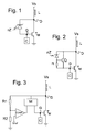
- a first solution provides one or more Zener diodes connected between the control terminal of the driving transistor and the inductive load.
- the Zeners constitute the reference for the voltage in this case, the maximum voltage being a combination of the Zener voltages.
- the inductive load L is connected in a low-side driver configuration, it having one terminal connected to the supply line Vs and the other terminal to the drain terminal D of a MOS driving transistor, here an N-channel type denoted by TM.
- the transistor TM has its source terminal connected to ground.
- Connected in series between the gate G and the node D, are a number, n, of Zener diodes schematically indicated at nZ in the Figure.
- a drawback of this circuit is that the maximum voltage value on the inductor, as determined by the combination of a discrete number of Zener voltages, may not equal exactly the desired one. In the instance of an integrated circuit, it should not be overlooked, moreover, that if the maximum voltage value is fairly high -- and fairly large, therefore, the number of the Zeners -- the area occupied by the recycling regulating circuit is better than negligible. The voltage value of the Zener diodes also is liable, as is well recognized, to be indeterminate due to significant process spread.
- the recycling regulating circuit further comprises at least one transistor Q of the bipolar type, connected between the gate G and the node D.
- the Zener diodes nZ are here connected between the base and the collector of the transistor Q.
- VBE is the drop in potential between the base and the emitter of the transistor Q.
- the transistor Q functions to absorb possible excess currents and prevent the Zener from being burned.
- the resistor R depicted in series with the Zener diodes in that Figure, is also effective to limit the current.
- one conventional circuit design provides for the use of a recycling regulating circuit which includes a voltage divider and a comparator.
- a circuit of that kind is disclosed in European Patent Application EP-0622717 by this Applicant.
- Such a circuit is illustrated in schematic form by Figure 3.
- the voltage divider R1-R2 is connected between the inductive load L and a ground terminal.
- the comparator COMP has two inputs respectively connected to the output of the voltage divider and to a generator of a reference voltage Vref, and has an output coupled to the gate terminal G of the driving transistor TM.
- the circuit further comprises a current mirror M having an input leg connected to the output of the comparator COMP and an output leg connected to the gate terminal G. The mirror M is also supplied to the node D.
- the reference voltage is compared with a divided value of the voltage to be regulated which is present on the node D.
- the reference for the voltage comprises that voltage reference circuit and the divider. Since the variation in the maximum voltage depends on a voltage reference which can be easily selected to be a stable one temperature-wise, that recycling regulating circuit is quite stable temperature-wise.
- the systems to be specifically discussed in connection with the invention include, as previously mentioned, a plurality of inductors.
- a plurality of inductors For example, in the instance of plural automotive devices wherein the different inductive loads require driving on an individual basis and must be operated each independently of the others, the recycling of the discharge current from each load should take place at different times from the other loads, and the discharging time required may not be the same for all the loads.
- the reference for the voltage may be provided in any desired way.
- circuits incorporating Zeners like those shown in Figures 1 and 2 are used.
- the overall number of Zeners employed actually tends to be fairly large.
- the number of the Zeners may be of about ten in each series, at the aforementioned maximum voltage values, which means that a very large area of the integrated circuit will be occupied.
- the technical problem that underlies this invention is to provide a circuit for independently recycling a plurality of inductive loads connected between two power supply terminals, which circuit can be integrated monolithically within a small integration area.
- An object of this invention is to provide a recycling circuit which is stable to variations in ambient conditions, such as temperature, and to varying parameters during its manufacture.
- the solvent idea on which the invention stands is that of providing a recycling circuit for plural inductive loads, which comprises, for each inductive load, at least one circuit element which allows the turning on of the driving element of one load to be uncoupled from that of the others. In this way, independent recycling of each load can be ensured while using a single common reference.
- a preferably monolithically integrated circuit for controllably and independently recycling the discharge current of a plurality of inductive loads connected between first and second power supply terminals comprises, for each of the loads, an active element and a regulator means for controlling the recycling of the discharge current of a respective one of the loads.
- the active element is connected in series with the inductive load between the two supply terminals, and has a control terminal to which a driver circuit is connected and which is coupled through an impedance to the supply terminal of lower potential.
- the regulator means is connected to the control terminal of the active element and to a node for connection between the active element and the respective inductive load.
- the recycling circuit includes a single voltage reference Vref.
- the regulator means for recycling control includes a blocking and triggering element and a circuit means for generating a turn-on signal to be applied to the control terminal of the active element.
- the blocking and triggering element is connected to the voltage reference, which is common for the whole circuit, and is coupled to the node for connection to the load.
- This circuit means is connected to the control terminal and operatively connected to the blocking and triggering element. Preferably, it is also connected to the node for connection.
- the blocking and triggering element will act on the circuit means to generate the turn-on signal and only start the recycling of the current through the active element when the potential at the node for connection to the load is significantly higher in absolute value than the reference potential. Otherwise, the blocking and triggering element would block the flow of current through said circuit means.
- the blocking and triggering element is essentially to permit the control terminal of the active elements for the different inductive loads to be uncoupled by acting thereon as a sensor of the voltage value present on the node for connection and as a recycling activator.
- the circuit means for generating the turn-on signal comprises a current mirror.
- the blocking and triggering element is preferably a diode which will be forward biased when the potential at the terminal for connection to the respective load is significantly higher in absolute value than the reference potential.
- Shown in Figure 4 is a comprehensive block diagram of a device which includes a circuit for controllably and independently recycling the discharge current of a plurality of inductive loads embodying this invention.
- the figure shows a number, N, of inductive loads L1, L2,...,LN connected between first and second power supply terminals which are respectively kept at constant voltages Va and Vb.
- the number N is illustratively on the order of a few tens.
- the lines Va and Vb typically represent power supply and ground lines. Both the low-side configuration, with Va corresponding to the supply voltage, and the high-side configuration, with the supply line being denoted by Vb, are encompassed by this invention.
- the circuit is preferably an integrated circuit and has a number, N, of terminals D1, D2,...,DN for connection to the inductive loads.
- the active element Tn is connected to the respective node Dn and the supply terminal Vb.
- a regulator means schematically represented by the block 2n, for controlling the recycling of the discharge current of the inductive load Ln, is connected to the node Dn and the control terminal DRn of the active element Tn.
- the regulator means 2n is further connected to a reference circuit, to be also indicated as the potential reference hereinafter, which generates a reference voltage Vref within the circuit 1.
- the inductive load Ln driving takes place directly through the active element Tn, functioning as a switch to regulate the flow of current through the respective load.
- a driver circuit Cn is operatively connected to a control terminal DRn of the active element Tn to alternatively drive it on and off.
- the driver circuits operate independently to permit operation of the N inductive loads. In practice, each circuit Cn acts on its corresponding active element and the latter, once turned on, forces a current flow through the inductor Ln.
- the regulator means 2n Upon the driver circuit Cn cutting off the flow of current through the inductive load Ln, and the current must then be flowed back as described, the regulator means 2n will allow the current to be recycled from the inductive load Ln through Tn. Specifically, the regulator means 2n functions as a sensor of the voltage value present on the specific node Dn for connection and determines the way that the corresponding active element Tn is to be turned back on, based upon a comparison with the value of the reference voltage Vref.
- FIG. 5 shows the inductive load L1, by way of example, but the scheme applies equally well to each of the other loads.
- the regulator means 21 comprises, in accordance with this invention, a blocking and triggering element 31 which is connected to the potential reference Vref and coupled to the node D1 for connection between the active element T1 and the inductive load L1.
- a circuit means 41 connected to the control terminal DR1 is arranged to generate a turn-on signal for application to the control terminal DR1. This is operatively acted upon by the blocking and triggering element 31.
- this circuit means is powered via the node D1 for connection.
- the circuit of Figure 5 operates as follows.
- the voltage at the node D1 which would be raised on account of the abrupt interruption in the current flow caused by the active element T1 being turned off, can attain a predetermined value VmaxD1 which is related to the reference value Vref.
- the element 31 will at that point be acting on the circuit means 41 to cause generation of the above turn-on signal.
- This signal generated by the circuit means 41 again enables the flow of current through the active element T1, with consequent discharging of the inductive load.
- the blocking and triggering element 31 performs a comparison of the potential present on the node for connection D1 with the constant value Vref. It is only activated when the potential at the node D1 is significantly higher in absolute value than the reference potential Vref. On the other hand, as long as the potential on the node D1 keeps within accettable values, i.e. below VmaxD1, the element 31 will function as a blocking element to inhibit operation of the means 41.
- the reference for the voltage according to this invention consists basically of the potential reference Vref; that is, the maximum voltage value for recycling triggering is substantially dependent on the value of Vref.
- the blocking and triggering element 31 functions to uncouple the control terminal DR1 of the active element T1 from the potential reference Vref. Accordingly, all the control terminals DRn will be uncoupled from one another. This allows a single voltage reference to be provided within the driver circuit 1 of the N inductive loads, while ensuring independent triggering for the different active elements Tn, with the latter being each allowed to recycle whenever necessary.
- the potential reference Vref is preferably included into the circuit, as shown in Figure 4. This reference may be provided by any generator of a constant voltage.
- the voltage Vref may be derived from the output of a voltage regulating circuit, or of a band-gap type of voltage multiplier. Also notice that the value of the voltage Vref may be either positive or negative, depending on specific applications.
- control terminal DR1 of the active element T1 is further coupled to the lower supply voltage terminal through an impedance Z1, as shown in Figure 5.
- the latter may represent one or more resistive loads.
- Z1 may comprise one or more capacitive loads.
- the circuit for recycling the N loads makes for a smaller bulk or occupied area than in the conventional circuit designs previously discussed. This because it is unnecessary to provide a number N of references for the voltage, as already explained.
- the blocking and triggering elements 3n and circuit means 4n may be small in size, as explained hereinafter in connection with one embodiment.
- the recycling circuit embodying this invention is advantageously stable, in that the maximum voltage value for recycling triggering is mainly dependent on the reference Vref.
- the potential reference may be selected to be uniquely stable to changes in ambient conditions, in particular to be unaffected by temperature.
- the operational conditions for the circuit triggering are made independent of random parameters.
- FIG. 6 A wiring diagram is specifically depicted in Figure 6 for a preferred embodiment.
- the blocks shown in the preceding figures have been denoted by the same references for clarity.
- the embodiment of figure 6 shows the N inductive loads Ln connected in a low-side driver configuration, that is with one terminal connected to a supply line Vs and the other terminal to the respective node Dn for connection between the load Ln and the circuit 1.
- N 8
- the description to follow will refer to a portion of the circuit 1 relating to a single inductive load, the first load L1, for example.
- the active element T1 for driving the load L1 comprises an N-channel MOS transistor. Preferably, this would be a power transistor in applications where the inductive load driving current is fairly large.
- the transistor T1 has a drain terminal connected to the node D1 and a source terminal to ground.
- the regulator means 21 for recycling control comprises a diode DI1 having its cathode connected to the potential reference Vref and its anode connected to an input leg of a current mirror, also included in the block 21 and comprising a pair of bipolar transistors Q11 and Q21 both of which are of the pnp type in this embodiment.
- An output leg of the current mirror Q11-Q21 is connected to the control terminal DR1, specifically comprised of a gate terminal of the transistor T1.
- the current mirror as shown in Figure 6 is preferably powered via the node D1 for connection between the circuit and the load L1.
- the gate terminal of the transistor T1 is also coupled to ground through a resistive load R1.
- the load R1 shown represents schematically one or more resistors in series.
- a driver circuit, illustrated in Figures 4 and 5 by the block C1 and also acting on the gate terminal DR1, is omitted from Figure 6.
- VmaxD1 Vref+VDI1+Vbe(Q11)
- VDI1 the voltage drop across the diode DI1 in conduction
- Vbe(Q11) the potential difference between the base and the emitter of the transistor Q11, as connected in a diode configuration.
- the value of Vmax is approximately equal to the value of Vref with the diode DI1 and current mirror conducting.
- the diode DI1 will actually be conducting because a voltage is present between its anode and cathode terminals which is equal to the forward biasing voltage.
- a current is caused to flow through the input leg of the current mirror Q11-Q21, from the potential reference through the diode DI1, which is mirrored onto the output leg.
- the current mirror supplies current to the resistor R1 and turns on again the transistor T1, biasing its gate DR1.
- the diode DI1 In a condition of no recycling, such as when the transistor T1 is on and a current is flowing through the load L1, the diode DI1 functions to block the current flow, the drain terminal of the transistor T1, and therefore the node D1, being in this case at a low voltage.
- the voltage on the anode of the diode DI1 is far lower than the cathode voltage, i.e. than Vref, so that the diode will block the flow of current. Accordingly, the transistors Q11 and Q21 of the current mirror will be in the off state.
- the diode DI1 functions as a blocking and triggering element, and is encircled by a dash line 31 in the Figure.
- this element 31 may be implemented in some other ways, provided that it will only supply current when the potential on its anode, or else on the node connected to the current mirror input, is significantly higher in absolute value than that on its cathode, but for the intrinsic voltage drop across the element 31 itself.
- the current mirror Q11-Q21 is generally shown at 41; it constitutes a preferential embodiment of the circuit means for generating the transistor T1 turn-on signal for recycling triggering.
- the turn-on signal consists in this case of the output current from the current mirror.
- the current mirror can optionally supply an amplified current.
- the current mirror should be capable of operating on a high voltage, since it is connected to that node.
- the circuit construction of the current mirror Q11-Q21 could be implemented in any other ways.
- the transistors Q11 and Q21 are not required to be of the bipolar type, and the mirror may be implemented with MOS technology, for example. Nor is it necessary that the mirror be powered from just D1.
- the active element T1 illustratively comprised of a MOS transistor could be replaced by a different active element, e.g. a Darlington.
- the preferred embodiment shown in Figure 6 of the recycling circuit 1, where the latter is advantageously in the integrated form would occupy a greatly reduced area because it includes a reduced number of transistors, and a definitely smaller area than the conventional circuits previously described.
- the recycling control afforded by the circuit shown in Figure 6 is advantageously unaffected by fluctuations in such external parameters as temperature and fabrication, because the values VmaxDn are mainly dependent on the voltage Vref, as previously explained.
- the contribution from the diodes DIn and the current mirror toward setting the value VmaxDn is a substantially stable one to temperature and unaffected by process parameters.
Landscapes
- Electronic Switches (AREA)
Priority Applications (3)
| Application Number | Priority Date | Filing Date | Title |
|---|---|---|---|
| DE69534839T DE69534839D1 (de) | 1995-07-31 | 1995-07-31 | Schaltung zum gesteuerten unabhängigen Verbrauchen von gespeicherter induktiver Energie mehrerer induktiver Lasten |
| EP95830344A EP0757443B1 (fr) | 1995-07-31 | 1995-07-31 | Circuit pour la dissipation contrôlée et indépendante d'énergie accumulée inductive des charges inductives multiples |
| US08/688,490 US5883537A (en) | 1995-07-31 | 1996-07-30 | Circuit and method for controlled independent recycle of discharge current of multiple inductive loads |
Applications Claiming Priority (1)
| Application Number | Priority Date | Filing Date | Title |
|---|---|---|---|
| EP95830344A EP0757443B1 (fr) | 1995-07-31 | 1995-07-31 | Circuit pour la dissipation contrôlée et indépendante d'énergie accumulée inductive des charges inductives multiples |
Publications (2)
| Publication Number | Publication Date |
|---|---|
| EP0757443A1 true EP0757443A1 (fr) | 1997-02-05 |
| EP0757443B1 EP0757443B1 (fr) | 2006-03-08 |
Family
ID=8221991
Family Applications (1)
| Application Number | Title | Priority Date | Filing Date |
|---|---|---|---|
| EP95830344A Expired - Lifetime EP0757443B1 (fr) | 1995-07-31 | 1995-07-31 | Circuit pour la dissipation contrôlée et indépendante d'énergie accumulée inductive des charges inductives multiples |
Country Status (3)
| Country | Link |
|---|---|
| US (1) | US5883537A (fr) |
| EP (1) | EP0757443B1 (fr) |
| DE (1) | DE69534839D1 (fr) |
Cited By (2)
| Publication number | Priority date | Publication date | Assignee | Title |
|---|---|---|---|---|
| WO2015062902A1 (fr) * | 2013-10-29 | 2015-05-07 | Robert Bosch Gmbh | Circuit de protection contre des surtensions pour un semi-conducteur de puissance et procédé de protection d'un semi-conducteur de puissance contre des surtensions |
| EP3089367A1 (fr) * | 2015-04-27 | 2016-11-02 | Renesas Electronics Corporation | Circuit de calage des tensions pour un élément semi-conducteur |
Families Citing this family (30)
| Publication number | Priority date | Publication date | Assignee | Title |
|---|---|---|---|---|
| DE19704089C2 (de) * | 1997-02-04 | 1999-02-11 | Deutsch Zentr Luft & Raumfahrt | Verfahren zur Steuerung eines Zerhacker(Chopper)-Treibers und Schaltungsanordnung zur Durchführung des Verfahrens |
| US6614633B1 (en) * | 1999-03-19 | 2003-09-02 | Denso Corporation | Semiconductor device including a surge protecting circuit |
| FR2811090B1 (fr) * | 2000-06-28 | 2002-10-11 | St Microelectronics Sa | Integration d'un regulateur de tension |
| JP3935777B2 (ja) * | 2002-05-28 | 2007-06-27 | 富士通株式会社 | 出力回路装置 |
| EP1443649B1 (fr) * | 2003-01-31 | 2008-08-13 | STMicroelectronics S.r.l. | Configuration de commutation par l'émetteur et structure intégrée correspondante |
| US7134959B2 (en) * | 2003-06-25 | 2006-11-14 | Scientific Games Royalty Corporation | Methods and apparatus for providing a lottery game |
| US7364091B2 (en) | 2003-12-19 | 2008-04-29 | Scientific Games International, Inc. | Embedded optical signatures in documents |
| DE102004007208B3 (de) * | 2004-02-13 | 2005-05-25 | Infineon Technologies Ag | Schaltungsanordnung mit einem Lasttransistor und einer Spannungsbegrenzungsschaltung und Verfahren zur Ansteuerung eines Lasttransistors |
| US7621814B2 (en) * | 2004-07-22 | 2009-11-24 | Scientific Games International, Inc. | Media enhanced gaming system |
| US7410168B2 (en) | 2004-08-27 | 2008-08-12 | Scientific Games International, Inc. | Poker style scratch-ticket lottery games |
| US7429044B2 (en) | 2004-08-31 | 2008-09-30 | Scientific Games International, Inc. | Scratch-ticket lottery and promotional games |
| WO2006042171A2 (fr) | 2004-10-11 | 2006-04-20 | Scientific Games Royalty Corporation | Jeu de loterie sportive a cote fixe |
| US7631871B2 (en) * | 2004-10-11 | 2009-12-15 | Scientific Games International, Inc. | Lottery game based on combining player selections with lottery draws to select objects from a third set of indicia |
| MX2007005181A (es) | 2004-10-28 | 2007-06-20 | Scient Games Royalty Corp | Juego de loteria jugando en una figura geometrica utilizando indicios con valores de punto variable. |
| US20060217181A1 (en) * | 2004-10-28 | 2006-09-28 | Chantal Jubinville | On-line lottery extension game having an instant component and a draw-based component |
| US7213811B2 (en) * | 2004-12-08 | 2007-05-08 | Scientific Games Royalty Corporation | Extension to a lottery game for which winning indicia are set by selections made by winners of a base lottery game |
| EP1861184A4 (fr) * | 2005-01-07 | 2009-05-13 | Scient Games Int Inc | Jeu de loterie utilisant des themes de jeu nostalgiques |
| US7662038B2 (en) * | 2005-01-07 | 2010-02-16 | Scientific Games International, Inc. | Multi-matrix lottery |
| CN101163527A (zh) * | 2005-01-11 | 2008-04-16 | 科学游戏程序国际有限公司 | 其中补充的彩票选择的标记可用于购买的联机彩票游戏 |
| US7601059B2 (en) | 2005-01-21 | 2009-10-13 | Scientific Games International, Inc. | Word-based lottery game |
| US7481431B2 (en) * | 2005-02-01 | 2009-01-27 | Scientific Games International, Inc. | Bingo-style lottery game ticket |
| US8262453B2 (en) * | 2005-02-09 | 2012-09-11 | Scientific Games International, Inc. | Combination lottery and raffle game |
| US8221210B2 (en) * | 2005-03-08 | 2012-07-17 | Scientific Games International, Inc. | Lottery game having secondary game with multiplier and second payout |
| US7874902B2 (en) * | 2005-03-23 | 2011-01-25 | Scientific Games International. Inc. | Computer-implemented simulated card game |
| US7867075B2 (en) * | 2005-04-27 | 2011-01-11 | Scientific Games International, Inc. | Game apparatus |
| US7654529B2 (en) | 2005-05-17 | 2010-02-02 | Scientific Games International, Inc. | Combination scratch ticket and on-line game ticket |
| AU2012203559B2 (en) * | 2007-11-23 | 2015-09-17 | Aristocrat Technologies Australia Pty Limited | A gaming system and a method of gaming |
| US8460081B2 (en) | 2010-05-14 | 2013-06-11 | Scientific Games International, Inc. | Grid-based multi-lottery game and associated method |
| US8808080B2 (en) | 2010-05-14 | 2014-08-19 | Scientific Games International, Inc. | Grid-based lottery game and associated method |
| US10666146B2 (en) * | 2018-03-05 | 2020-05-26 | Texas Instruments Incorporated | Bidirectional inverting buck-boost converter converting dissipation current into recycling current |
Citations (5)
| Publication number | Priority date | Publication date | Assignee | Title |
|---|---|---|---|---|
| US4679112A (en) * | 1986-07-31 | 1987-07-07 | General Motors Corporation | Transistor protection circuit for automotive motor control applications |
| FR2593946A1 (fr) * | 1986-01-24 | 1987-08-07 | Peugeot | Regulateur de tension |
| FR2654880A1 (fr) * | 1989-11-22 | 1991-05-24 | Siemens Automotive Sa | Circuit integre de puissance "intelligent" du type mos, pour la commande de l'alimentation d'une charge electrique. |
| EP0525522A2 (fr) * | 1991-07-31 | 1993-02-03 | STMicroelectronics S.r.l. | Dispositif de détection de défauts pour circuit d'attaque |
| EP0622717A1 (fr) * | 1993-04-30 | 1994-11-02 | STMicroelectronics S.r.l. | Circuit à récirculation de courant de décharge de charge inductive avec compensation en température |
Family Cites Families (4)
| Publication number | Priority date | Publication date | Assignee | Title |
|---|---|---|---|---|
| DE4236334A1 (de) * | 1992-10-28 | 1994-05-05 | Bosch Gmbh Robert | Monolithisch integriertes MOS-Endstufenbauteil mit einer Überlast-Schutzeinrichtung |
| JP3084982B2 (ja) * | 1992-11-25 | 2000-09-04 | 富士電機株式会社 | 半導体装置 |
| US5416361A (en) * | 1993-09-02 | 1995-05-16 | At&T Corp. | Low dissipation snubber for switching power transistor |
| EP0677925B1 (fr) * | 1994-04-12 | 1998-10-07 | STMicroelectronics S.r.l. | Dispositif électronique de puissance à porte isolée à trois bornes avec une caractéristique de saturation de sortie à pente variable fonction discontinue du courant de sortie |
-
1995
- 1995-07-31 DE DE69534839T patent/DE69534839D1/de not_active Expired - Lifetime
- 1995-07-31 EP EP95830344A patent/EP0757443B1/fr not_active Expired - Lifetime
-
1996
- 1996-07-30 US US08/688,490 patent/US5883537A/en not_active Expired - Lifetime
Patent Citations (5)
| Publication number | Priority date | Publication date | Assignee | Title |
|---|---|---|---|---|
| FR2593946A1 (fr) * | 1986-01-24 | 1987-08-07 | Peugeot | Regulateur de tension |
| US4679112A (en) * | 1986-07-31 | 1987-07-07 | General Motors Corporation | Transistor protection circuit for automotive motor control applications |
| FR2654880A1 (fr) * | 1989-11-22 | 1991-05-24 | Siemens Automotive Sa | Circuit integre de puissance "intelligent" du type mos, pour la commande de l'alimentation d'une charge electrique. |
| EP0525522A2 (fr) * | 1991-07-31 | 1993-02-03 | STMicroelectronics S.r.l. | Dispositif de détection de défauts pour circuit d'attaque |
| EP0622717A1 (fr) * | 1993-04-30 | 1994-11-02 | STMicroelectronics S.r.l. | Circuit à récirculation de courant de décharge de charge inductive avec compensation en température |
Cited By (5)
| Publication number | Priority date | Publication date | Assignee | Title |
|---|---|---|---|---|
| WO2015062902A1 (fr) * | 2013-10-29 | 2015-05-07 | Robert Bosch Gmbh | Circuit de protection contre des surtensions pour un semi-conducteur de puissance et procédé de protection d'un semi-conducteur de puissance contre des surtensions |
| US10236874B2 (en) | 2013-10-29 | 2019-03-19 | Robert Bosch Gmbh | Overvoltage protection circuit for a power semiconductor and method for protecting a power semiconductor from over-voltages |
| EP3089367A1 (fr) * | 2015-04-27 | 2016-11-02 | Renesas Electronics Corporation | Circuit de calage des tensions pour un élément semi-conducteur |
| CN106089462A (zh) * | 2015-04-27 | 2016-11-09 | 瑞萨电子株式会社 | 半导体装置、功率控制半导体装置、车载电子控制单元及车辆 |
| JP2016208406A (ja) * | 2015-04-27 | 2016-12-08 | ルネサスエレクトロニクス株式会社 | 半導体装置、電力制御用半導体装置、車載用電子制御ユニット及びそれを備えた車両 |
Also Published As
| Publication number | Publication date |
|---|---|
| US5883537A (en) | 1999-03-16 |
| DE69534839D1 (de) | 2006-05-04 |
| EP0757443B1 (fr) | 2006-03-08 |
Similar Documents
| Publication | Publication Date | Title |
|---|---|---|
| EP0757443B1 (fr) | Circuit pour la dissipation contrôlée et indépendante d'énergie accumulée inductive des charges inductives multiples | |
| EP0585926B1 (fr) | Dispositif à semiconducteur à grille isolée | |
| US5796276A (en) | High-side-driver gate drive circuit | |
| KR100264718B1 (ko) | 조정기회로및반도체집적회로장치 | |
| US7619450B2 (en) | Start-up circuit for providing a start-up voltage to an application circuit | |
| EP0501418B1 (fr) | Régulateur de tension a faible chute de tension. | |
| EP0622717A1 (fr) | Circuit à récirculation de courant de décharge de charge inductive avec compensation en température | |
| JPH06244693A (ja) | Mos電界効果トランジスタスイッチ回路 | |
| US4611162A (en) | Parallel voltage regulators with different operating characteristics collectively forming a single regulator with wide operating range | |
| US6870351B2 (en) | Voltage regulator circuit and integrated circuit device including the same | |
| US5748422A (en) | Power latch circuit with overvoltage protection | |
| EP0427086B1 (fr) | Circuit de décharge de grille adaptative pour transistors à effet de champ de puissance | |
| US4683438A (en) | Circuit for connecting a load to the high side of a DC power supply | |
| US4513241A (en) | Foldback current limiting driver | |
| EP0631375B1 (fr) | Etage de sortie alternativement utilisant un appareil MOS ou bipolaire, dépendant de la tension d'alimentation et régulateur pour un alternateur | |
| JP2719677B2 (ja) | 誘導負荷駆動のための能動過電圧コントロール回路 | |
| JPH03159561A (ja) | スイツチングレギユレータ用回路装置 | |
| JP4082547B2 (ja) | 発光素子の電源供給制御装置 | |
| GB2170931A (en) | Driver circuit for solenoids | |
| KR100213582B1 (ko) | 전원공급장치에 연결되는 공진부하를 구동하는 모놀리식반도체 전원장치의 출력전압을 제한하기 위한 회로 | |
| US4400756A (en) | Inductive load driver protection circuits having minimal power dissipation | |
| KR101325184B1 (ko) | 과전압 보호 회로 및 이를 구비한 반도체 장치 | |
| JP3232981B2 (ja) | 制御信号のレベルシフト回路 | |
| JP2026044327A (ja) | 電源回路 | |
| SU320880A1 (ru) | Устройство защиты |
Legal Events
| Date | Code | Title | Description |
|---|---|---|---|
| PUAI | Public reference made under article 153(3) epc to a published international application that has entered the european phase |
Free format text: ORIGINAL CODE: 0009012 |
|
| AK | Designated contracting states |
Kind code of ref document: A1 Designated state(s): DE FR GB IT |
|
| 17P | Request for examination filed |
Effective date: 19970728 |
|
| RAP3 | Party data changed (applicant data changed or rights of an application transferred) |
Owner name: STMICROELECTRONICS S.R.L. |
|
| 17Q | First examination report despatched |
Effective date: 20020711 |
|
| GRAP | Despatch of communication of intention to grant a patent |
Free format text: ORIGINAL CODE: EPIDOSNIGR1 |
|
| GRAS | Grant fee paid |
Free format text: ORIGINAL CODE: EPIDOSNIGR3 |
|
| GRAA | (expected) grant |
Free format text: ORIGINAL CODE: 0009210 |
|
| AK | Designated contracting states |
Kind code of ref document: B1 Designated state(s): DE FR GB IT |
|
| PG25 | Lapsed in a contracting state [announced via postgrant information from national office to epo] |
Ref country code: IT Free format text: LAPSE BECAUSE OF FAILURE TO SUBMIT A TRANSLATION OF THE DESCRIPTION OR TO PAY THE FEE WITHIN THE PRE;WARNING: LAPSES OF ITALIAN PATENTS WITH EFFECTIVE DATE BEFORE 2007 MAY HAVE OCCURRED AT ANY TIME BEFORE 2007. THE CORRECT EFFECTIVE DATE MAY BE DIFFERENT FROM THE ONE RECORDED.SCRIBED TIME-LIMIT Effective date: 20060308 |
|
| REG | Reference to a national code |
Ref country code: GB Ref legal event code: FG4D |
|
| REF | Corresponds to: |
Ref document number: 69534839 Country of ref document: DE Date of ref document: 20060504 Kind code of ref document: P |
|
| PG25 | Lapsed in a contracting state [announced via postgrant information from national office to epo] |
Ref country code: DE Free format text: LAPSE BECAUSE OF FAILURE TO SUBMIT A TRANSLATION OF THE DESCRIPTION OR TO PAY THE FEE WITHIN THE PRESCRIBED TIME-LIMIT Effective date: 20060609 |
|
| PGFP | Annual fee paid to national office [announced via postgrant information from national office to epo] |
Ref country code: GB Payment date: 20060627 Year of fee payment: 12 |
|
| PLBE | No opposition filed within time limit |
Free format text: ORIGINAL CODE: 0009261 |
|
| STAA | Information on the status of an ep patent application or granted ep patent |
Free format text: STATUS: NO OPPOSITION FILED WITHIN TIME LIMIT |
|
| 26N | No opposition filed |
Effective date: 20061211 |
|
| EN | Fr: translation not filed | ||
| GBPC | Gb: european patent ceased through non-payment of renewal fee |
Effective date: 20070731 |
|
| PG25 | Lapsed in a contracting state [announced via postgrant information from national office to epo] |
Ref country code: FR Free format text: LAPSE BECAUSE OF FAILURE TO SUBMIT A TRANSLATION OF THE DESCRIPTION OR TO PAY THE FEE WITHIN THE PRESCRIBED TIME-LIMIT Effective date: 20070309 |
|
| PG25 | Lapsed in a contracting state [announced via postgrant information from national office to epo] |
Ref country code: GB Free format text: LAPSE BECAUSE OF NON-PAYMENT OF DUE FEES Effective date: 20070731 |
|
| PG25 | Lapsed in a contracting state [announced via postgrant information from national office to epo] |
Ref country code: FR Free format text: LAPSE BECAUSE OF FAILURE TO SUBMIT A TRANSLATION OF THE DESCRIPTION OR TO PAY THE FEE WITHIN THE PRESCRIBED TIME-LIMIT Effective date: 20060308 |