EP0757458A2 - Bittakterfassungsverfahren und -anordnung für Direktsequenzspreizspektrumempfänger - Google Patents
Bittakterfassungsverfahren und -anordnung für Direktsequenzspreizspektrumempfänger Download PDFInfo
- Publication number
- EP0757458A2 EP0757458A2 EP96305590A EP96305590A EP0757458A2 EP 0757458 A2 EP0757458 A2 EP 0757458A2 EP 96305590 A EP96305590 A EP 96305590A EP 96305590 A EP96305590 A EP 96305590A EP 0757458 A2 EP0757458 A2 EP 0757458A2
- Authority
- EP
- European Patent Office
- Prior art keywords
- signal
- magnitudes
- samples
- bit
- sum
- Prior art date
- Legal status (The legal status is an assumption and is not a legal conclusion. Google has not performed a legal analysis and makes no representation as to the accuracy of the status listed.)
- Withdrawn
Links
Images


Classifications
-
- H—ELECTRICITY
- H03—ELECTRONIC CIRCUITRY
- H03L—AUTOMATIC CONTROL, STARTING, SYNCHRONISATION OR STABILISATION OF GENERATORS OF ELECTRONIC OSCILLATIONS OR PULSES
- H03L7/00—Automatic control of frequency or phase; Synchronisation
-
- H—ELECTRICITY
- H04—ELECTRIC COMMUNICATION TECHNIQUE
- H04B—TRANSMISSION
- H04B1/00—Details of transmission systems, not covered by a single one of groups H04B3/00 - H04B13/00; Details of transmission systems not characterised by the medium used for transmission
- H04B1/69—Spread spectrum techniques
- H04B1/707—Spread spectrum techniques using direct sequence modulation
- H04B1/7073—Synchronisation aspects
- H04B1/7075—Synchronisation aspects with code phase acquisition
- H04B1/70755—Setting of lock conditions, e.g. threshold
-
- H—ELECTRICITY
- H04—ELECTRIC COMMUNICATION TECHNIQUE
- H04L—TRANSMISSION OF DIGITAL INFORMATION, e.g. TELEGRAPHIC COMMUNICATION
- H04L7/00—Arrangements for synchronising receiver with transmitter
- H04L7/0054—Detection of the synchronisation error by features other than the received signal transition
-
- H—ELECTRICITY
- H04—ELECTRIC COMMUNICATION TECHNIQUE
- H04B—TRANSMISSION
- H04B2201/00—Indexing scheme relating to details of transmission systems not covered by a single group of H04B3/00 - H04B13/00
- H04B2201/69—Orthogonal indexing scheme relating to spread spectrum techniques in general
- H04B2201/707—Orthogonal indexing scheme relating to spread spectrum techniques in general relating to direct sequence modulation
- H04B2201/70707—Efficiency-related aspects
Definitions
- This invention relates to systems and methods for receiving signals having data coded therein, and in particular to systems and methods for determining and/or adjusting a clock used to extract the data from a received signal.
- signals to be transmitted in which data to be transmitted is used to modify a carrier signal.
- digital data may be used to key a phase shift keyed modulator of a carrier frequency.
- Decoding of such modulated signals generally requires acquisition and tracking of the carrier frequency and demodulating of the carrier signal to return the original data signal.
- the demodulating may take more than one step as the received signal may first be down converted to an intermediate frequency and subsequently demodulated to baseband.
- This baseband signal may then be processed in a correlator to remove an overlying spectrum spreading pseudo noise sequence.
- Such sequences are well known in the art and are referred to as spread spectrum. They are often applied as phase shift keyed ("PSK”) modulation over the data modulation.
- PSK phase shift keyed
- the spreading sequence usually has a higher rate than the data modulation, often much higher.
- the data signal may be a series of transitions in phase or amplitude or frequency, each transition signifying the transmission of one or more portions of the data signal.
- the carrier signal is phase shift keyed to represent the data.
- the modulating signal causes the phase of the carrier signal to be advanced (or retarded) a predetermined number of degrees of phase to represent either a 0 or 1 binary number.
- the carrier signal contains one "symbol" which may represent one or more bits of data.
- the modulating signal is applied to the carrier signal without regard to the phase relationship between the two signals.
- the receiver may not necessarily know therefrom the beginning of each symbol within the data signal.
- the presence of noise on the received signal may make it difficult to determine from examining any particular symbol where the symbol begins.
- the receiver In order to demodulate a received signal in straightforward fashion, the receiver should know the modulation rate, i.e., how often to expect to receive a new symbol. Accordingly, the receiver may be set to generate a clock pulse the frequency of which coincides with the frequency of the modulation (or the symbol rate). This clock may be called a bit clock because it has a frequency which should match the frequency at which new symbols are received. Oftentimes, the receiver may also generate other clocks as needed from the bit clock. Merely having a bit clock, however, is generally insufficient because the bit clock must usually be synchronized with the incoming symbols. Unless the bit clock is properly synchronized, decoding and demodulating components the signal may suffer relatively large losses.
- bit synchronization In the case of spread spectrum, demodulating the signal is generally possible only if the bit clock is aligned such that the signal samples being used fall somewhere on the correlation peak. Once bit synchronization can be obtained, however, the various receiver elements can be set to align the decoding circuits so that decoding and similar evaluations of the received symbols may be accomplished at the most useful time within the symbol period (For example, the bit synchronization may be critical in determining when to use an analog-to-digital circuit to sample the magnitude of the input signal.)
- a received signal may be sampled at a frequency greater than the Nyquist frequency and the digital samples represent the received signal.
- a sequence of symbols may be represented by a sequence of samples.
- the sequence of digital samples may be evaluated to locate which set of the samples best coincides with an event expected within each symbol (start, end, transition, etc.).
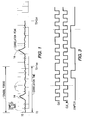
- a received signal 10 after correlation processing, may have the shape shown.
- Samples 12 of the signal are taken at a periodic rate and digitally stored and processed.
- peaks 14 in the signal represent the points of maximum correlation between the PN reference and the signal spreading sequence for each symbol.
- a receiver can determine where the peaks 14 occur and adjust its decoding circuits to center the peaks within the symbol period. For the signal of Figure 1, the peaks occur near the eighth sample, and accordingly, the eighth sample will have the maximum value. The decode circuitry can then be reset to center the symbol period appropriately.
- An object of the present invention is to provide a method and apparatus of acquiring bit synchronization while minimizing additional circuitry and power consumption, and to acquire bit synchronization with a reduced number of circuit components and complexity when compared to some prior art bit synchronization schemes.
- Another object is to provide a method and apparatus for demodulating and decoding phase shift keyed signals without a relatively high speed A-to-D device to adjust bit synchronization.
- a circuit for acquiring the bit synchronization of a signal having plural symbols contained therein comprising:
- the present invention also includes a method A method for acquiring bit timing in a received signal comprising the steps of:
- the invention furthermore, includes a signal processing system for a signal having plural symbols within a predetermined interval of time, a system for synchronizing the decoding of the symbols comprising:
- PN pseudorandom noise
- Figure 1 illustrates a process to a received spread signal digitally.
- one typical step is to correlate the PN code against the received signal to develop a correlated signal 10.
- the correlated signal 10 indicates the locations along the received signal where the data signals are present.
- the correlation process produces a correlated signal in which triangular peaks 14 occur at the data locations. The higher the peak within the signal, the better the correlation between the received signal and the PN code.
- messages are transmitted in the form of plural, periodic symbols modulated onto a carrier signal, a series of peaks 14 will be output from the correlator at the frequency of the modulating signal.
- the task of the bit synchronization circuit is to identify the locations of the peak and to adjust the decoding and demodulating circuits to the extent possible to perform their decoding/demodulating functions as near to the center of the peaks as possible, within the cost, size, and power constraints applicable to a particular receiving system.
- the output of the correlator circuit may be digitized at a periodic rate greater than the bit rate. For example, in the system shown in Figure 1, each bit period is sampled twenty-two times to produce twenty-two samples per symbol.
- a receiving system can determine that the symbols are best decoded with respect to a particular sample within each symbol period. So long as the symbol clock of the receiving system matches the symbol clock of the transmitting system, the location of the sample within each symbol which has the highest correlation value will remain the same over plural symbols. (Clock drift or noise may eventually cause the location of the sample having the highest value to drift or change within a particular message).
- the sampling of the correlator signal 10 is depicted in greater detail at and near the peak 14 of the signal. Note that no sample 12 occurs exactly at the peak correlation magnitude.
- the sample having the highest correlation magnitude is the S sample; the sample immediately earlier than the S sample is designated as the E sample (or early sample); and, the sample immediately after the highest sample is designated the L sample (or late sample).
- the sample (or bit) clock is aligned exactly with the received signal. In this situation, the magnitudes of the early sample and the late sample would be expected to be nearly equal and be nearly 50% of the magnitude of the S sample.
- Figure 2 shows the S sample is not taken at exactly the point of highest correlation and the early and late samples are not equal to each other. This relationship among the early, largest and late samples may be used to adjust the bit synchronization with respect to the symbol timing of the received signal.
- the bit synchronization (“sync”) clock used to clock the symbol decode and demodulate circuits is simply adjusted to bring into better alignment the receiver bit clock and the symbols in the received signal. It is known to use a periodic signal such as a sinusoid or square wave to drive the devices, such as the A/D converters which sample the received signal or signals derived therefrom, such as a correlation signal.
- the sampling circuit may be built such that a sample is taken upon the occurrence (a rising edge, a falling edge, etc.) of the bit clock.
- the bit clock can be operated at a frequency such that the rising edges of the bit clock occur, and drive the synchronization circuits, at a rising edge of the system clock.
- the bit clock can be made to better coincide with the received symbol clocking by selectively inverting the bit clock (to delay one-half cycle of the clock) and/or by selectively inverting and skipping one cycle of the clock (to advance the clock by one-half cycle).
- Figure 3 shows a receiver using conventional means to generate a clocking signal which produces a clock signal of a desired frequency (the expected frequency of the symbols).
- the signal labelled CLK_IN is such a signal.
- the CLK_IN signal is used by appropriate circuitry to produce a signal CLK (a bit sync clock) which may be used to drive the decode and demodulation circuits.
- a delay of one-half cycle in the clock signal is desirable to align the bit sync clock with the symbols of the received signal, such a delay can be accomplished by selectively inverting the CLK signal. If a signal JUMPCLK is received, indicating that the CLK should be inverted, a selectively operated inversion device can be placed between the CLK_IN signal and the CLK signal derived therefrom to invert the CLK signal. When the CLK signal is so inverted, its rising edges are thereafter delayed one-half cycle from when they otherwise would have occurred. At another selective time, the CLK signal may be again inverted to again delay the CLK signal by one half-cycle.
- the circuit determines that a one-half cycle advance of the CLK signal is needed, an entire cycle of the CLK signal can be skipped and the signal inverted to effective advance the CLK signal by one-half cycle.
- the advancement of the CLK circuit can readily be performed by appropriate circuits in the CLK generating circuit or by circuit elements which use the CLK signal.
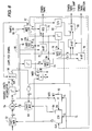
- Figure 4 illustrates a circuit which can be used to delay the CLK circuit by one-half cycle may include an Exclusive-OR gate EO which receives a CLK_IN signal and a signal from a first D-Q flip-flop 20.
- the CLK_IN signal may be a periodic signal, such as the square wave signal referenced as CLK_IN of Figure 3.
- the EO Exclusive-OR gate produces a signal CLK_EO which is applied to one input gate of a first OR gate 22.
- the other input into the first OR gate 22 is tied to the clock input of the first D-Q flip-flop 20.
- the output signal 24 is taken at the output of the first OR gate 22.
- a signal indicating when the output clock signal is to be inverted may be received at a circuit input JUMPCLK.
- the JUMPCLK signal is applied to the D lead of a second D-Q flip-flop 28 and to one of the inputs of an AND gate 30.
- the second D-Q flip-flop 28 is clocked by the CLK-EO signal.
- the output signal from the first D-Q flip-flop 20 is provided to the second input of the AND gate 30.
- the output of the AND gate 30 is provided to a SR latch 32 which has its output tied to a third D-Q flip-flop 36.
- the output signal from the third D-Q flip-flop 36 is tied back to the input of the S-R gate 32 and is also provided to the clock lead of the first D-Q flip-flop 20.
- the output signal from the third D-Q flip-flop 36 is used to clock the first D-Q flip-flop 20, as a second input signal to the first OR gate 22, and as the second input to the SR latch 32.
- a CLK_IN signal may be provided to the first input of the Exclusive OR gate EO. SO long as the other input of the Exclusive OR gate EO remains low, the periodic signal of the CLK_IN signal is passed through to the first OR gate 22, and ultimately, assuming a zero input on the other input to the first OR gate 22, the CLK-IN signal is passed out of the circuit as the CLK signal 24.
- a pulse signal may be provided on the JUMPCLK signal. Note that the length of the pulse is not significant as only the leading (rising) edge of the JUMPCLK signal affects the circuit of Figure 4.
- a circuit of the present invention causes a graceful inversion of the CLK signal upon receipt of a rising edge on the JUMPCLK line and causes a second inversion (to the original phase relationship) upon receipt of a second rising edge on the JUMPCLK line.
- Appropriate reset inputs to the gates in the circuit of Figure 4 may be used to obtain a known initial condition upon reinitialization of the circuit.
- the bit sync clock adjustment circuit of Figure 4 may be used along with suitable other circuits to determine the samples within a series of sampled symbols at which decoding should be accomplished and to adjust the bit synchronization of the decoding and demodulating circuits to better center the sampling near the received peak of the symbol.
- Figure 5 shows a functional block diagram of a system which could be used to adjust the bit synchronization may receive a signal which provides a time series of magnitudes associated with each sample of a received signal.
- the magnitude signal may be provided to an accumulator 42 which sums the magnitudes associated with each sample position within a symbol. For example, the accumulator may sum all the first samples (within each symbol) together, all the second samples together, etc. for a predetermined period of time.
- the period of time over which the samples are accumulated may be a function of the duration of the preamble or a portion of a preamble of the received signal.
- the sums are evaluated by a biggest selector 44 which compares the accumulated sums and determines which set of samples contains the highest sum.
- the set of samples having the biggest sum and the adjacent samples i.e., the early and late samples are then passed to an adjacent sample comparator 46 which determines the extent to which the selected biggest set of samples are centered in the peak of the received signal and whether an adjustment in the bit sync clock is desirable.
- bits indicating that fact and the direction of the adjustment may be sent to a bit sync adjust circuit 48 which adjusts the bit sync clock with respect to the received signal.
- the bit sync adjust circuit 48 may include a circuit such as depicted in Figure 4 to adjust the bit sync clock.
- the adjacent sample comparator 46 may evaluate the biggest set of samples and the adjacent sets of samples to determine if and how much bit sync adjustment may be desirable.
- the adjacent sample comparator may look at the magnitudes of the adjacent sets of samples in relation to the magnitude of the biggest set of samples. For example, the comparator could compare the summed magnitudes and if either of the adjacent samples magnitudes exceeds a threshold, the bit sync clock can be adjusted to move the bit sync clock one half-cycle between the biggest set of samples and the next biggest magnitude samples. It has been determined that the comparator circuit works appropriately when the comparator compares the magnitude of the adjacent set of samples to determine whether either adjacent set has a total magnitude at or exceeding seventy-five percent (75%) of the magnitude of the biggest set of samples.
- Figure 6 is one embodiment of a circuit which can carry out the bit clock synchronization portion of the present invention may receive an input signal 50 indicating the magnitude of samples of the received signal (or of correlations between the received signal and a PN code) which may be applied to a shifting multiplexer 52.
- the output of the shifting multiplexer 52 may be applied in turn to a summer 54, a variable length accumulator 56 and a multiplexer 58.
- the multiplexer 58 may be set to operate based on the number of chips (or samples) per symbol within the received signal.
- a sample clock signal 60 operating at the frequency of the sampling, may be used to provide a clocking signal to the variable length accumulator and to a modulo counter 62 which repeatedly counts from one to the number of samples per symbol, i.e., the modulo counter 62 identifies the position of each sample within a symbol.
- a second shifting multiplexer 64 also feeds the summer 54 to accumulate the magnitude associated with each sample position within a symbol.
- the results from the variable length accumulator are read into a biggest picker circuit 66.
- the biggest picker circuit 66 includes a largest register used to hold the largest sum of magnitudes value received from the variable length accumulator.
- a corresponding register 70 holds the position (or timing) within the symbols of the sample having the largest magnitude sum.
- the biggest picker 66 will have within its circuits the largest value sample, the values of the adjacent samples, and the position or timing of the largest value.
- the two adjacent values may be compared first with each other in a second comparator 78 to determine which sample is larger and then the larger of the two adjacent samples is compared in a third comparator against a scaled value of the largest sample.
- the scaling of the largest sample is accomplished in a scaler 82 which may be set, for example, to 0.75 to compare the adjacent sample against 75 % of the largest sample.
- the timing of the sample having the largest cumulative value is already in the corresponding register 70 and may be made available (through the SYMBOL TIMING signal) to other elements within the receiver for decoding and demodulating the symbols.
- a signal is sent to the bit sync circuit to adjust the bit sync timing by one-half sample (SYMBOL TIMING 1/2 SAMP) and the direction (early or late) in which to adjust the bit sync timing (SYMBOL TIMING DIRECTION).
- the main sample clock may be inverted as discussed earlier with regard to Figure 4. If a timing advance of one-half cycle is desired, the clock may be inverted, as explained previously, and the timing decode circuits may be advanced by an entire clock cycle. This technique advances the symbol interval by one-half clock cycle without requiring any circuit to run at twice speed.
- the magnitude signals contain up to eights bits of value. If two such magnitude values are added, the sum of the values may overflow an eight bit register. In conventional magnitude comparing circuits, the accumulator and many other devices must be more than eight bits in width or the selection of the biggest sum of magnitudes will be erroneous. In one aspect of the present invention, overflow is avoided yet additional circuitry to widen the bit width of the accumulator and downstream circuits is not required. To avoid the overflow, after each magnitude is added to the running total of each sample, the most significant bit of the total is checked to determine whether it is set by a flip-flop 82. If the bit is set, the flip-flop is used to enable a counter 84 which tracks the number of times that the magnitude has been shifted within the evaluation period.
- the counter 84 also causes the two shifting multiplexers 52 and 64 to right shift their contents using a barrel shift.
- all of the samples are scaled equally and both the stored partial magnitude sums and the input values are scaled in a corresponding manner.
- signals having a relatively large strength (and correspondingly large correlation magnitudes) will not overflow the accumulator and both the stored values and the input values will be shifted in a coordinated manner.
- signals having low magnitudes scaling, and its usual lose of precision may be avoided.
- the magnitude values 50 output from a correlator may be accumulated for fourteen symbols.
- the accumulator and the various counters may previously have been be cleared (by the BS-CL) signal at the beginning of an evaluation interval.
- the accumulator length (i.e., the number of samples which can be processed in parallel) may, if desired, be set to correspond to the number of samples per symbol by use of the mux 58 which can be selected from one of a predefined set of available selections.
- an apparatus for obtaining and adjusting bit synchronization In a direct sequence spread spectrum receiver, an apparatus for obtaining and adjusting bit synchronization.
- the bit synchronization is adjusted by selectively inverting a clocking circuit to delay sampling by one-half a clock cycle and to combine the inversion with a skipping of one cycle to advance the sampling by one-half cycle.
- the synchronization circuit avoids overflow of accumulating components by downshifting both the partial sums and the input data when needed.
Landscapes
- Engineering & Computer Science (AREA)
- Computer Networks & Wireless Communication (AREA)
- Signal Processing (AREA)
- Synchronisation In Digital Transmission Systems (AREA)
- Dc Digital Transmission (AREA)
Applications Claiming Priority (2)
| Application Number | Priority Date | Filing Date | Title |
|---|---|---|---|
| US08/509,588 US5654991A (en) | 1995-07-31 | 1995-07-31 | Fast acquisition bit timing loop method and apparatus |
| US509588 | 1995-07-31 |
Publications (2)
| Publication Number | Publication Date |
|---|---|
| EP0757458A2 true EP0757458A2 (de) | 1997-02-05 |
| EP0757458A3 EP0757458A3 (de) | 2000-01-05 |
Family
ID=24027291
Family Applications (1)
| Application Number | Title | Priority Date | Filing Date |
|---|---|---|---|
| EP96305590A Withdrawn EP0757458A3 (de) | 1995-07-31 | 1996-07-30 | Bittakterfassungsverfahren und -anordnung für Direktsequenzspreizspektrumempfänger |
Country Status (4)
| Country | Link |
|---|---|
| US (1) | US5654991A (de) |
| EP (1) | EP0757458A3 (de) |
| JP (1) | JPH09153887A (de) |
| KR (1) | KR100433751B1 (de) |
Cited By (5)
| Publication number | Priority date | Publication date | Assignee | Title |
|---|---|---|---|---|
| WO2000035140A1 (en) * | 1998-12-08 | 2000-06-15 | Ericsson Inc. | Synchronization tracking method |
| WO2001020841A1 (en) * | 1999-09-10 | 2001-03-22 | Telefonaktiebolaget L M Ericsson | Technique for demodulating a linear modulated data signal in a communications system |
| WO2005048521A1 (en) * | 2003-08-28 | 2005-05-26 | Qualcomm Incorporated | Bit synchronization in a communications device |
| EP1703661A1 (de) * | 2005-03-14 | 2006-09-20 | NTT DoCoMo INC. | Mobiles Telekommunikationsendgerät mit Kontrolle der Abtastphase |
| EP1703660A1 (de) * | 2005-03-14 | 2006-09-20 | NTT DoCoMo Inc. | Abtastratensteuerung in einem mobilen Kommunikationsendgerät |
Families Citing this family (15)
| Publication number | Priority date | Publication date | Assignee | Title |
|---|---|---|---|---|
| JP2926651B2 (ja) * | 1995-11-02 | 1999-07-28 | 株式会社鷹山 | マッチドフィルタ回路 |
| US6243372B1 (en) * | 1996-11-14 | 2001-06-05 | Omnipoint Corporation | Methods and apparatus for synchronization in a wireless network |
| US6266172B1 (en) * | 1997-11-06 | 2001-07-24 | Agere Systems Optoelectronics Guardian Corp. | Signal bit rate and performance measurement for optical channel signals |
| US6421371B1 (en) | 1998-11-17 | 2002-07-16 | Ericsson Inc. | Modulation sequence synchronization methods and apparatus employing partial sequence correlation |
| FI114887B (fi) * | 1999-10-13 | 2005-01-14 | U Nav Microelectronics Corp | Hajaspektrivastaanottimen signaalinhakujärjestelmä |
| US7231000B2 (en) | 2001-10-22 | 2007-06-12 | Broadcom Corporation | System and method for DC offset compensation and bit synchronization |
| US20050047537A1 (en) * | 2003-08-29 | 2005-03-03 | Ting-Yuan Cheng | Method and system of signal path tracking |
| JP4097615B2 (ja) * | 2004-03-23 | 2008-06-11 | 三洋電機株式会社 | 信号検出方法および装置ならびにそれを利用した送信装置および受信装置 |
| JP4308105B2 (ja) * | 2004-08-23 | 2009-08-05 | Okiセミコンダクタ株式会社 | 同期追従回路 |
| US8542714B2 (en) * | 2005-07-29 | 2013-09-24 | U-Blox Ag | Method and system for reconstructing time of transmit from assisted or weak signal GPS observations |
| KR100653199B1 (ko) * | 2005-11-18 | 2006-12-05 | 삼성전자주식회사 | 로컬 신호를 이용하여 수신 신호에서 리키지 성분을제거하는 rf 수신 장치 및 방법 |
| US20110134906A1 (en) * | 2009-12-03 | 2011-06-09 | Qualcomm Incorporated | Method and apparatus for distributed processing for wireless sensors |
| WO2011096025A1 (ja) * | 2010-02-04 | 2011-08-11 | パナソニック電工株式会社 | 遅延検波回路および受信装置 |
| CN119341653A (zh) | 2019-04-12 | 2025-01-21 | 迈凌有限公司 | 用于nrz调制光纤传输的电双二进制软信息接收器 |
| WO2025019836A2 (en) * | 2023-07-19 | 2025-01-23 | Maxlinear, Inc. | Low complexity soft decision optical receiver |
Family Cites Families (10)
| Publication number | Priority date | Publication date | Assignee | Title |
|---|---|---|---|---|
| MX157636A (es) * | 1984-01-03 | 1988-12-07 | Motorola Inc | Mejoras en circuito de sincronizacion de fase digital de frecuencia multiple |
| US4653076A (en) * | 1984-03-23 | 1987-03-24 | Sangamo Weston, Inc. | Timing signal correction system for use in direct sequence spread signal receiver |
| US4805191A (en) * | 1987-11-25 | 1989-02-14 | Motorola, Inc. | Modem with improved timing recovery using equalized data |
| US5140617A (en) * | 1990-02-07 | 1992-08-18 | Mitsubishi Denki Kabushiki Kaisha | Frame phase estimation method and circuit |
| US5056054A (en) * | 1990-05-02 | 1991-10-08 | National Semiconductor Corporation | Digital phase locked loop utilizing a multi-bit phase error input for control of a stepped clock generator |
| US5280501A (en) * | 1990-10-09 | 1994-01-18 | Seko Corp. | Data bit synchronization |
| US5199050A (en) * | 1991-04-05 | 1993-03-30 | Trw Inc. | Pseudorandom (PN) signal synchronization circuit and related method |
| US5325405A (en) * | 1991-08-27 | 1994-06-28 | Motorola, Inc. | Burst mode receiver control |
| GB2276797B (en) * | 1993-04-02 | 1996-10-23 | Northern Telecom Ltd | Digital demodulation |
| US5499273A (en) * | 1995-05-11 | 1996-03-12 | Motorola, Inc. | Method and apparatus for symbol clock recovery from signal having wide frequency possibilities |
-
1995
- 1995-07-31 US US08/509,588 patent/US5654991A/en not_active Expired - Lifetime
-
1996
- 1996-07-30 EP EP96305590A patent/EP0757458A3/de not_active Withdrawn
- 1996-07-31 JP JP8202384A patent/JPH09153887A/ja active Pending
- 1996-07-31 KR KR1019960032113A patent/KR100433751B1/ko not_active Expired - Lifetime
Non-Patent Citations (1)
| Title |
|---|
| None |
Cited By (14)
| Publication number | Priority date | Publication date | Assignee | Title |
|---|---|---|---|---|
| CN1319310C (zh) * | 1998-12-08 | 2007-05-30 | 艾利森公司 | 同步跟踪方法 |
| US6314148B1 (en) | 1998-12-08 | 2001-11-06 | Ericsson Inc | Synchronization tracking method |
| WO2000035140A1 (en) * | 1998-12-08 | 2000-06-15 | Ericsson Inc. | Synchronization tracking method |
| WO2001020841A1 (en) * | 1999-09-10 | 2001-03-22 | Telefonaktiebolaget L M Ericsson | Technique for demodulating a linear modulated data signal in a communications system |
| US6904104B1 (en) | 1999-09-10 | 2005-06-07 | Telefonaktiebolaget L M Ericsson (Publ) | Technique for demodulating a linear modulated data signal in a communications system |
| WO2005048521A1 (en) * | 2003-08-28 | 2005-05-26 | Qualcomm Incorporated | Bit synchronization in a communications device |
| US7248624B2 (en) | 2003-08-28 | 2007-07-24 | Qualcomm Incorporated | Bit synchronization in a communications device |
| EP1703660A1 (de) * | 2005-03-14 | 2006-09-20 | NTT DoCoMo Inc. | Abtastratensteuerung in einem mobilen Kommunikationsendgerät |
| EP1755254A1 (de) * | 2005-03-14 | 2007-02-21 | NTT DoCoMo Inc. | Mobiles Telekommunikationsendgerät mit Kontrolle der Abtastphase |
| EP1755255A1 (de) * | 2005-03-14 | 2007-02-21 | NTT DoCoMo Inc. | Mobiles Telekommunikationsendgerät mit Kontrolle der Abtastphase |
| EP1703661A1 (de) * | 2005-03-14 | 2006-09-20 | NTT DoCoMo INC. | Mobiles Telekommunikationsendgerät mit Kontrolle der Abtastphase |
| US7602871B2 (en) | 2005-03-14 | 2009-10-13 | Ntt Docomo, Inc. | Mobile communication terminal |
| US7706491B2 (en) | 2005-03-14 | 2010-04-27 | Ntt Docomo, Inc. | Mobile communication terminal |
| CN1835430B (zh) * | 2005-03-14 | 2012-02-08 | 株式会社Ntt都科摩 | 移动通信终端 |
Also Published As
| Publication number | Publication date |
|---|---|
| EP0757458A3 (de) | 2000-01-05 |
| JPH09153887A (ja) | 1997-06-10 |
| KR970008905A (ko) | 1997-02-24 |
| KR100433751B1 (ko) | 2004-08-18 |
| US5654991A (en) | 1997-08-05 |
Similar Documents
| Publication | Publication Date | Title |
|---|---|---|
| US5654991A (en) | Fast acquisition bit timing loop method and apparatus | |
| US5093841A (en) | Clock acquisition in a spread spectrum system | |
| EP0701333B1 (de) | Verfahren und Gerät zur Synchronisierung in einem Direktsequenzspreizspektrumkommunikationssystem | |
| US6614864B1 (en) | Apparatus for and method of adaptive synchronization in a spread spectrum communications receiver | |
| EP0583241B1 (de) | Spreizspektrumkorrelator | |
| CA2105299C (en) | Asymmetric spread spectrum correlator | |
| US5237587A (en) | Pseudo-noise modem and related digital correlation method | |
| US6064695A (en) | Spread spectrum communication system utilizing differential code shift keying | |
| US4964138A (en) | Differential correlator for spread spectrum communication system | |
| US7006587B1 (en) | Preamble aided synchronization | |
| US5761211A (en) | Peak correlation timing recovery circuit and receiving apparatus | |
| US5719900A (en) | Dual-threshold spread spectrum correlator | |
| US20030156672A1 (en) | Frame synchronization and detection technique for a digital receiver | |
| US6212223B1 (en) | Demodulation and correlation for spread spectrum communications | |
| JP2002501713A (ja) | バーストタイプ・ディジタル通信システムのためのプリアンブル検出と情報伝送を組合せる方法 | |
| JP4557486B2 (ja) | 差分符号シフトキーイングを利用するスペクトラム拡散通信システム | |
| US5103465A (en) | Symbol synchronization circuit | |
| US3931472A (en) | Asynchronous quadriphase communications system and method | |
| EP1176732A2 (de) | Verfahren und Gerät zur Kodenachführung in einem Rake-Empfänger | |
| KR100534592B1 (ko) | 디지털 통신 시스템의 수신 장치 및 그 방법 | |
| US6940837B1 (en) | Spread spectrum demodulator | |
| JP3406167B2 (ja) | 同期装置 | |
| JP2999368B2 (ja) | 同期装置 | |
| JP3693516B2 (ja) | スペクトル拡散通信機 | |
| US7023906B2 (en) | Receiver and receiving method in spread spectrum communication system |
Legal Events
| Date | Code | Title | Description |
|---|---|---|---|
| PUAI | Public reference made under article 153(3) epc to a published international application that has entered the european phase |
Free format text: ORIGINAL CODE: 0009012 |
|
| AK | Designated contracting states |
Kind code of ref document: A2 Designated state(s): DE FR GB IT |
|
| RIC1 | Information provided on ipc code assigned before grant |
Free format text: 6H 04L 7/033 A, 6H 04J 13/00 B, 6H 04L 7/04 B |
|
| PUAL | Search report despatched |
Free format text: ORIGINAL CODE: 0009013 |
|
| AK | Designated contracting states |
Kind code of ref document: A3 Designated state(s): DE FR GB IT |
|
| 17P | Request for examination filed |
Effective date: 20000705 |
|
| 17Q | First examination report despatched |
Effective date: 20061115 |
|
| STAA | Information on the status of an ep patent application or granted ep patent |
Free format text: STATUS: THE APPLICATION IS DEEMED TO BE WITHDRAWN |
|
| 18D | Application deemed to be withdrawn |
Effective date: 20070201 |