EP0758143B1 - Procédés améliorés pour masquage pendant la fabrication d'un dispositif semi-conducteur - Google Patents
Procédés améliorés pour masquage pendant la fabrication d'un dispositif semi-conducteur Download PDFInfo
- Publication number
- EP0758143B1 EP0758143B1 EP96111988A EP96111988A EP0758143B1 EP 0758143 B1 EP0758143 B1 EP 0758143B1 EP 96111988 A EP96111988 A EP 96111988A EP 96111988 A EP96111988 A EP 96111988A EP 0758143 B1 EP0758143 B1 EP 0758143B1
- Authority
- EP
- European Patent Office
- Prior art keywords
- substrate
- growth
- semiconductor devices
- masking
- during fabrication
- Prior art date
- Legal status (The legal status is an assumption and is not a legal conclusion. Google has not performed a legal analysis and makes no representation as to the accuracy of the status listed.)
- Expired - Lifetime
Links
Images
Classifications
-
- H—ELECTRICITY
- H10—SEMICONDUCTOR DEVICES; ELECTRIC SOLID-STATE DEVICES NOT OTHERWISE PROVIDED FOR
- H10P—GENERIC PROCESSES OR APPARATUS FOR THE MANUFACTURE OR TREATMENT OF DEVICES COVERED BY CLASS H10
- H10P76/00—Manufacture or treatment of masks on semiconductor bodies, e.g. by lithography or photolithography
- H10P76/40—Manufacture or treatment of masks on semiconductor bodies, e.g. by lithography or photolithography of masks comprising inorganic materials
- H10P76/405—Manufacture or treatment of masks on semiconductor bodies, e.g. by lithography or photolithography of masks comprising inorganic materials characterised by their composition, e.g. multilayer masks
-
- H—ELECTRICITY
- H10—SEMICONDUCTOR DEVICES; ELECTRIC SOLID-STATE DEVICES NOT OTHERWISE PROVIDED FOR
- H10P—GENERIC PROCESSES OR APPARATUS FOR THE MANUFACTURE OR TREATMENT OF DEVICES COVERED BY CLASS H10
- H10P14/00—Formation of materials, e.g. in the shape of layers or pillars
- H10P14/20—Formation of materials, e.g. in the shape of layers or pillars of semiconductor materials
- H10P14/24—Formation of materials, e.g. in the shape of layers or pillars of semiconductor materials using chemical vapour deposition [CVD]
-
- H—ELECTRICITY
- H10—SEMICONDUCTOR DEVICES; ELECTRIC SOLID-STATE DEVICES NOT OTHERWISE PROVIDED FOR
- H10P—GENERIC PROCESSES OR APPARATUS FOR THE MANUFACTURE OR TREATMENT OF DEVICES COVERED BY CLASS H10
- H10P14/00—Formation of materials, e.g. in the shape of layers or pillars
- H10P14/20—Formation of materials, e.g. in the shape of layers or pillars of semiconductor materials
- H10P14/27—Formation of materials, e.g. in the shape of layers or pillars of semiconductor materials using selective deposition, e.g. simultaneous growth of monocrystalline and non-monocrystalline semiconductor materials
- H10P14/271—Formation of materials, e.g. in the shape of layers or pillars of semiconductor materials using selective deposition, e.g. simultaneous growth of monocrystalline and non-monocrystalline semiconductor materials characterised by the preparation of substrate for selective deposition
-
- H—ELECTRICITY
- H10—SEMICONDUCTOR DEVICES; ELECTRIC SOLID-STATE DEVICES NOT OTHERWISE PROVIDED FOR
- H10P—GENERIC PROCESSES OR APPARATUS FOR THE MANUFACTURE OR TREATMENT OF DEVICES COVERED BY CLASS H10
- H10P14/00—Formation of materials, e.g. in the shape of layers or pillars
- H10P14/20—Formation of materials, e.g. in the shape of layers or pillars of semiconductor materials
- H10P14/27—Formation of materials, e.g. in the shape of layers or pillars of semiconductor materials using selective deposition, e.g. simultaneous growth of monocrystalline and non-monocrystalline semiconductor materials
- H10P14/276—Lateral overgrowth
-
- H—ELECTRICITY
- H10—SEMICONDUCTOR DEVICES; ELECTRIC SOLID-STATE DEVICES NOT OTHERWISE PROVIDED FOR
- H10P—GENERIC PROCESSES OR APPARATUS FOR THE MANUFACTURE OR TREATMENT OF DEVICES COVERED BY CLASS H10
- H10P14/00—Formation of materials, e.g. in the shape of layers or pillars
- H10P14/20—Formation of materials, e.g. in the shape of layers or pillars of semiconductor materials
- H10P14/29—Formation of materials, e.g. in the shape of layers or pillars of semiconductor materials characterised by the substrates
- H10P14/2901—Materials
- H10P14/2907—Materials being Group IIIA-VA materials
- H10P14/2908—Nitrides
-
- H—ELECTRICITY
- H10—SEMICONDUCTOR DEVICES; ELECTRIC SOLID-STATE DEVICES NOT OTHERWISE PROVIDED FOR
- H10P—GENERIC PROCESSES OR APPARATUS FOR THE MANUFACTURE OR TREATMENT OF DEVICES COVERED BY CLASS H10
- H10P14/00—Formation of materials, e.g. in the shape of layers or pillars
- H10P14/20—Formation of materials, e.g. in the shape of layers or pillars of semiconductor materials
- H10P14/29—Formation of materials, e.g. in the shape of layers or pillars of semiconductor materials characterised by the substrates
- H10P14/2901—Materials
- H10P14/2907—Materials being Group IIIA-VA materials
- H10P14/2911—Arsenides
-
- H—ELECTRICITY
- H10—SEMICONDUCTOR DEVICES; ELECTRIC SOLID-STATE DEVICES NOT OTHERWISE PROVIDED FOR
- H10P—GENERIC PROCESSES OR APPARATUS FOR THE MANUFACTURE OR TREATMENT OF DEVICES COVERED BY CLASS H10
- H10P14/00—Formation of materials, e.g. in the shape of layers or pillars
- H10P14/20—Formation of materials, e.g. in the shape of layers or pillars of semiconductor materials
- H10P14/29—Formation of materials, e.g. in the shape of layers or pillars of semiconductor materials characterised by the substrates
- H10P14/2901—Materials
- H10P14/2921—Materials being crystalline insulating materials
-
- H—ELECTRICITY
- H10—SEMICONDUCTOR DEVICES; ELECTRIC SOLID-STATE DEVICES NOT OTHERWISE PROVIDED FOR
- H10P—GENERIC PROCESSES OR APPARATUS FOR THE MANUFACTURE OR TREATMENT OF DEVICES COVERED BY CLASS H10
- H10P14/00—Formation of materials, e.g. in the shape of layers or pillars
- H10P14/20—Formation of materials, e.g. in the shape of layers or pillars of semiconductor materials
- H10P14/34—Deposited materials, e.g. layers
- H10P14/3402—Deposited materials, e.g. layers characterised by the chemical composition
- H10P14/3404—Deposited materials, e.g. layers characterised by the chemical composition being Group IVA materials
- H10P14/3408—Silicon carbide
-
- H—ELECTRICITY
- H10—SEMICONDUCTOR DEVICES; ELECTRIC SOLID-STATE DEVICES NOT OTHERWISE PROVIDED FOR
- H10P—GENERIC PROCESSES OR APPARATUS FOR THE MANUFACTURE OR TREATMENT OF DEVICES COVERED BY CLASS H10
- H10P14/00—Formation of materials, e.g. in the shape of layers or pillars
- H10P14/20—Formation of materials, e.g. in the shape of layers or pillars of semiconductor materials
- H10P14/34—Deposited materials, e.g. layers
- H10P14/3402—Deposited materials, e.g. layers characterised by the chemical composition
- H10P14/3404—Deposited materials, e.g. layers characterised by the chemical composition being Group IVA materials
- H10P14/3411—Silicon, silicon germanium or germanium
-
- H—ELECTRICITY
- H10—SEMICONDUCTOR DEVICES; ELECTRIC SOLID-STATE DEVICES NOT OTHERWISE PROVIDED FOR
- H10P—GENERIC PROCESSES OR APPARATUS FOR THE MANUFACTURE OR TREATMENT OF DEVICES COVERED BY CLASS H10
- H10P14/00—Formation of materials, e.g. in the shape of layers or pillars
- H10P14/20—Formation of materials, e.g. in the shape of layers or pillars of semiconductor materials
- H10P14/34—Deposited materials, e.g. layers
- H10P14/3402—Deposited materials, e.g. layers characterised by the chemical composition
- H10P14/3414—Deposited materials, e.g. layers characterised by the chemical composition being group IIIA-VIA materials
- H10P14/3418—Phosphides
-
- H—ELECTRICITY
- H10—SEMICONDUCTOR DEVICES; ELECTRIC SOLID-STATE DEVICES NOT OTHERWISE PROVIDED FOR
- H10P—GENERIC PROCESSES OR APPARATUS FOR THE MANUFACTURE OR TREATMENT OF DEVICES COVERED BY CLASS H10
- H10P14/00—Formation of materials, e.g. in the shape of layers or pillars
- H10P14/20—Formation of materials, e.g. in the shape of layers or pillars of semiconductor materials
- H10P14/34—Deposited materials, e.g. layers
- H10P14/3402—Deposited materials, e.g. layers characterised by the chemical composition
- H10P14/3414—Deposited materials, e.g. layers characterised by the chemical composition being group IIIA-VIA materials
- H10P14/3421—Arsenides
-
- H—ELECTRICITY
- H10—SEMICONDUCTOR DEVICES; ELECTRIC SOLID-STATE DEVICES NOT OTHERWISE PROVIDED FOR
- H10P—GENERIC PROCESSES OR APPARATUS FOR THE MANUFACTURE OR TREATMENT OF DEVICES COVERED BY CLASS H10
- H10P76/00—Manufacture or treatment of masks on semiconductor bodies, e.g. by lithography or photolithography
- H10P76/40—Manufacture or treatment of masks on semiconductor bodies, e.g. by lithography or photolithography of masks comprising inorganic materials
- H10P76/408—Manufacture or treatment of masks on semiconductor bodies, e.g. by lithography or photolithography of masks comprising inorganic materials characterised by their sizes, orientations, dispositions, behaviours or shapes
Definitions
- the present invention pertains to the fabrication of semiconductor devices and more specifically to improved masking techniques during semiconductor device fabrication.
- masking material e.g. photoresist or the like
- semiconductor material is grown over masked and unmasked areas.
- the material on the masked areas is then removed by etching and lift-off.
- material is selectively grown in unmasked areas and the masking material is then removed.
- One problem that arises is that the structure or substrate (generally a wafer) must be removed from the growth chamber to remove the masking material. The structure is then masked again and reintroduced into the growth chamber for re-growth.
- etching is required to remove unwanted material and masks are removed by etching, solvent, or the like.
- the material of the semiconductor device has a high likelihood of being contaminated by the etchant, which contamination greatly reduces the life of the device, the operating characteristics of the device, and the reliability of the device.
- the etching process severely damages semiconductor material adjacent the etched areas which further reduces life, operating characteristics, and reliability.
- etching processes are very time consuming and difficult to perform.
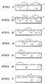
- FIGS. 1 - 4 illustrate several steps in a method of masking a substrate 10, in accordance with the present invention, for the fabrication of semiconductor devices.
- substrate 10 is formed of gallium arsenide (GaAs), but it will be understood by those skilled in the art that other materials known in the art might be utilized.
- GaAs gallium arsenide
- a thin layer 12 of native oxide is present on surface 11 of substrate 10 if the substrate has been exposed to air.
- the layer 12 of oxide is approximately 2 nm thick and forms on substrate 10 whenever it is exposed to air (ambient) for a short time.
- Oxide mask 15 may be simply a shadow or metal mask or it can be formed in the well known manner with photolithography.
- oxide mask 15 is positioned on surface 11, or on layer 12 of native oxide if it is present, so as to define one or more growth areas 16 on surface 11 beneath oxide mask 15 and one or more unmasked portions 17 on surface 11 of substrate 10.
- a second oxide layer 20 is grown on unmasked portions 17 of the native oxide (see FIG. 2) and, as will be understood by those skilled in the art, will form with the native oxide as a portion thereof.
- substrate 10 is exposed to an ultraviolet source in ambient conditions (air), i.e. no special chamber, etc., to expose the unmasked portions 17 of substrate 10 to a combination of ultraviolet rays and ozone.
- the UV-ozone process grows a much thicker and denser layer of oxide than the native oxide. While other methods of growing second oxide layer 20 may be devised and used, it should be understood that second oxide layer 20 is formed sufficiently thicker and denser than the native oxide so that selective removal of the native oxide can be accomplished, as will be explained presently.
- oxide mask 15 is removed to expose growth areas 16, as illustrated in FIG. 3.
- Substrate 10 is then introduced into a growth chamber (not shown) and heated to desorb any native oxide that may be present in growth areas 16. In the present example in which a gallium arsenide substrate is utilized, the substrate is heated in the growth chamber to approximately 580°C - 600°C to desorb the native oxide in the exposed growth area. Substrate 10 with oxide-free growth areas 16 is illustrated in FIG. 4.
- Material 25 can be lattice matched with the material of substrate 10, for instance, gallium arsenide is selectively grown at 570°C - 590°C and lattice matched to the gallium arsenide of substrate 10, indium arsenide is selectively grown at 500°C - 515°C, etc.
- oxide layer 20 in place as a mask for further growth, a predetermined amount of crystalline material 25 is selectively grown in area (or areas) 16.
- "selective growth” or “selectively grown” is defined as growing only in the specific or designated area.
- material 25 grows only in growth areas 16.
- material 25 generally grows in a crystalline form so that growth rates and shapes are crystallographic dependent, i.e. the rate and shape of growth are dependent upon the type of material 25 being utilized.
- substrate 10 is heated to a higher temperature under high group V flux in the growth chamber to desorb oxide layer 20.
- substrate 10 is heated to approximately 640°C under high arsenic flux.
- the higher arsenic flux prevents gallium arsenide desorption during the desorption of oxide layer 20, resulting in the structure illustrated in FIG. 6.
- the mask utilized for patterned growth of material 25 is desorbed, or removed, in situ, i.e. without the need to remove substrate 10 from the growth chamber.
- an improved masking processes which provides a new and improved method of masking substrates during semiconductor device fabrication.
- the new and improved method of masking substrates does not require removal of the substrate from the processing chamber to remove the mask. Because the new and improved method of masking substrates does not require the introduction and removal of wafers or substrates from processing chambers several times in sequence during the fabrication of semiconductor devices, the fabrication process is much simpler and includes less chance of contamination of the devices.
- the present novel process allows selective growth and further re-growth, all in-situ, without exposure to air and contamination during the intermediate processing steps between epitaxy, etc. By eliminating air and other contaminant exposure between steps, the novel process ensures good quality in subsequent epitaxial steps
Claims (6)
- Procédé de masquage de substrats pendant la fabrication de dispositifs à semiconducteur, qui comprend les opérations consistant à fournir un substrat (10) doté d'une surface plane (11), et à positionner un masque (15) sur la surface (11) de façon à définir une aire de croissance (16) et une partie non masquée (17) sur la surface (11) du substrat (10),
caractérisé par les opérations suivantes :faire croítre une couche d'oxyde (20) sur la partie non masquée (17) de la surface (11) en exposant le substrat (10) à une source de rayonnement ultraviolet dans l'air afin d'exposer la surface (11) à une combinaison de rayons ultraviolets et d'ozone ;retirer le masque (15) afin d'exposer l'aire de croissance (16) ;introduire le substrat (10) dans une chambre de croissance et faire sélectivement croítre, sur l'aire de croissance exposée (16), une matière cristalline (25) ; etchauffer le substrat (10) dans la chambre de croissance afin d'amener la désorption de la couche d'oxyde (20). - Procédé de masquage de substrats pendant la fabrication de dispositifs à semiconducteur selon la revendication 1, caractérisé en outre en ce que l'opération de chauffage du substrat (10) dans la chambre de croissance visant à faire désorber la couche d'oxyde (20) comporte le chauffage du substrat (10) à une température d'environ 640°C sous un flux élevé d'arsenic.
- Procédé de masquage de substrats pendant la fabrication de dispositifs à semiconducteur selon la revendication 1, caractérisé en outre en ce que l'opération de fourniture du substrat (10) comporte la fourniture d'un substrat (10) d'arséniure de gallium ayant une couche mince d'oxyde natif (12) à sa surface(11).
- Procédé de masquage de substrats pendant la fabrication de dispositifs à semiconducteur selon la revendication 3, caractérisé en outre en ce que l'opération d'introduction du substrat (10) dans la chambre de croissance comporte le chauffage du substrat (10) afin de faire désorber l'oxyde natif (12) dans l'aire de croissance exposée (16).
- Procédé de masquage de substrats pendant la fabrication de dispositifs à semiconducteur selon la revendication 4, caractérisé en outre en ce que l'opération de chauffage du substrat (10) visant à faire désorber l'oxyde natif (12) dans l'aire de croissance exposée (16) comporte le chauffage du substrat d'arséniure de gallium (10) dans la chambre de croissance à une température d'environ 580°C à 600°C.
- Procédé de masquage de substrats pendant la fabrication de dispositifs à semiconducteur selon la revendication 1, caractérisé en outre en ce que les opérations de fourniture d'un substrat (10) doté d'une surface plane (11), de positionnement d'un masque (15) sur la surface (11), et de croissance d'une couche d'oxyde (20) sur la partie non masquée (16) de la surface (11) s'effectuent à la température ambiante.
Applications Claiming Priority (2)
| Application Number | Priority Date | Filing Date | Title |
|---|---|---|---|
| US08/511,772 US5730798A (en) | 1995-08-07 | 1995-08-07 | Masking methods during semiconductor device fabrication |
| US511772 | 1995-08-07 |
Publications (2)
| Publication Number | Publication Date |
|---|---|
| EP0758143A1 EP0758143A1 (fr) | 1997-02-12 |
| EP0758143B1 true EP0758143B1 (fr) | 2002-02-20 |
Family
ID=24036372
Family Applications (1)
| Application Number | Title | Priority Date | Filing Date |
|---|---|---|---|
| EP96111988A Expired - Lifetime EP0758143B1 (fr) | 1995-08-07 | 1996-07-25 | Procédés améliorés pour masquage pendant la fabrication d'un dispositif semi-conducteur |
Country Status (4)
| Country | Link |
|---|---|
| US (2) | US5730798A (fr) |
| EP (1) | EP0758143B1 (fr) |
| JP (1) | JP3152877B2 (fr) |
| DE (1) | DE69619316T2 (fr) |
Families Citing this family (9)
| Publication number | Priority date | Publication date | Assignee | Title |
|---|---|---|---|---|
| US5709744A (en) * | 1996-03-01 | 1998-01-20 | Motorola | Masking methods during semiconductor device fabrication |
| FR2761811B1 (fr) * | 1997-04-03 | 1999-07-16 | France Telecom | Technologie sans gravure pour integration de composants |
| US6001722A (en) * | 1997-06-20 | 1999-12-14 | Motorola, Inc. | Selective metallization/deposition for semiconductor devices |
| US20110163323A1 (en) * | 1997-10-30 | 2011-07-07 | Sumitomo Electric Industires, Ltd. | GaN SINGLE CRYSTAL SUBSTRATE AND METHOD OF MAKING THE SAME |
| CA2311132C (fr) * | 1997-10-30 | 2004-12-07 | Sumitomo Electric Industries, Ltd. | Substrat monocristallin de gan et procede de production associe |
| US6091085A (en) * | 1998-02-19 | 2000-07-18 | Agilent Technologies, Inc. | GaN LEDs with improved output coupling efficiency |
| DE19922167A1 (de) * | 1999-05-12 | 2000-11-16 | Wacker Siltronic Halbleitermat | Verfahren zur Herstellung einer Halbleiterscheibe |
| US20010019135A1 (en) * | 1999-06-28 | 2001-09-06 | Tsui Raymond K. | Sparse-carrier devices and method of fabrication |
| US7440666B2 (en) * | 2004-02-25 | 2008-10-21 | Avago Technologies Fiber Ip (Singapore) Pte. Ltd. | Buried heterostucture device having integrated waveguide grating fabricated by single step MOCVD |
Family Cites Families (6)
| Publication number | Priority date | Publication date | Assignee | Title |
|---|---|---|---|---|
| GB1428769A (en) * | 1972-02-28 | 1976-03-17 | Nippon Sheet Glass Co Ltd | Surface protective coating on an article |
| US4472459A (en) * | 1983-10-24 | 1984-09-18 | Rca Corporation | Local oxidation of silicon substrate using LPCVD silicon nitride |
| US5571471A (en) * | 1984-08-08 | 1996-11-05 | 3D Systems, Inc. | Method of production of three-dimensional objects by stereolithography |
| US4717681A (en) * | 1986-05-19 | 1988-01-05 | Texas Instruments Incorporated | Method of making a heterojunction bipolar transistor with SIPOS |
| JPH06124892A (ja) * | 1992-09-28 | 1994-05-06 | Hikari Gijutsu Kenkyu Kaihatsu Kk | GaAs酸化膜のパターニング方法 |
| US5451425A (en) * | 1994-09-13 | 1995-09-19 | The United States Of America As Represented By The Secretary Of The Army | Process for setting the frequency of a silicon microresonator |
-
1995
- 1995-08-07 US US08/511,772 patent/US5730798A/en not_active Expired - Fee Related
-
1996
- 1996-07-25 DE DE69619316T patent/DE69619316T2/de not_active Expired - Fee Related
- 1996-07-25 EP EP96111988A patent/EP0758143B1/fr not_active Expired - Lifetime
- 1996-08-05 JP JP22178396A patent/JP3152877B2/ja not_active Expired - Fee Related
-
1997
- 1997-01-03 US US08/775,934 patent/US5846609A/en not_active Expired - Fee Related
Also Published As
| Publication number | Publication date |
|---|---|
| DE69619316D1 (de) | 2002-03-28 |
| JPH0950962A (ja) | 1997-02-18 |
| US5730798A (en) | 1998-03-24 |
| JP3152877B2 (ja) | 2001-04-03 |
| US5846609A (en) | 1998-12-08 |
| EP0758143A1 (fr) | 1997-02-12 |
| DE69619316T2 (de) | 2002-07-18 |
Similar Documents
| Publication | Publication Date | Title |
|---|---|---|
| US5700703A (en) | Method of fabricating buried control elements in semiconductor devices | |
| US4637129A (en) | Selective area III-V growth and lift-off using tungsten patterning | |
| JP3330218B2 (ja) | 半導体装置の製造方法,及び半導体装置 | |
| US4859618A (en) | Method of producing the gate electrode of a field effect transistor | |
| EP0758143B1 (fr) | Procédés améliorés pour masquage pendant la fabrication d'un dispositif semi-conducteur | |
| EP0783176B1 (fr) | Procédés améliorés de masquage pendant la fabrication de dispositifs semi-conducteurs | |
| US5114871A (en) | Manufacturing diamond electronic devices | |
| US5830801A (en) | Resistless methods of gate formation in MOS devices | |
| US5904552A (en) | Method of resistless patterning of a substrate for implantation | |
| US5204278A (en) | Method of making MES field effect transistor using III-V compound semiconductor | |
| US5877071A (en) | Masking methods during semiconductor device fabrication | |
| US5591666A (en) | Semiconductor device and method of fabrication | |
| US5709744A (en) | Masking methods during semiconductor device fabrication | |
| US6001722A (en) | Selective metallization/deposition for semiconductor devices | |
| US5837560A (en) | Method of masking substrates leaving exposed facets | |
| US5759880A (en) | Resistless methods of fabricating FETs | |
| JP2500443B2 (ja) | 化合物半導体のドライエッチング方法 | |
| JP3080860B2 (ja) | ドライエッチング方法 | |
| JP2699928B2 (ja) | 化合物半導体基板の前処理方法 | |
| JPH0218579B2 (fr) | ||
| JP2714703B2 (ja) | 選択エピタキシャル成長法 | |
| US5733817A (en) | Blanket oxidation for contact isolation | |
| ISHIKAWA et al. | Electron Beam Lithography Using GaAs Oxidized Resist for GaAs/AlGaAs Ultrafine Structure Fabrication | |
| EP0416924A2 (fr) | Procédé de fabrication de membres conducteurs sur une surface semi-conductrice | |
| EP0692818A2 (fr) | Procédé pour retirer la contamination et l'oxygène au cours de la fabrication de dispositifs semi-conducteurs, procédé de fabrication de composant à semi-conducteur composé et appareil associé |
Legal Events
| Date | Code | Title | Description |
|---|---|---|---|
| PUAI | Public reference made under article 153(3) epc to a published international application that has entered the european phase |
Free format text: ORIGINAL CODE: 0009012 |
|
| AK | Designated contracting states |
Kind code of ref document: A1 Designated state(s): DE FR GB |
|
| 17P | Request for examination filed |
Effective date: 19970812 |
|
| 17Q | First examination report despatched |
Effective date: 19990316 |
|
| RTI1 | Title (correction) |
Free format text: IMPROVED MASKING METHODS DURING SEMICONDUCTOR DEVICE FABRICATION |
|
| GRAG | Despatch of communication of intention to grant |
Free format text: ORIGINAL CODE: EPIDOS AGRA |
|
| GRAG | Despatch of communication of intention to grant |
Free format text: ORIGINAL CODE: EPIDOS AGRA |
|
| GRAH | Despatch of communication of intention to grant a patent |
Free format text: ORIGINAL CODE: EPIDOS IGRA |
|
| GRAH | Despatch of communication of intention to grant a patent |
Free format text: ORIGINAL CODE: EPIDOS IGRA |
|
| REG | Reference to a national code |
Ref country code: GB Ref legal event code: IF02 |
|
| GRAA | (expected) grant |
Free format text: ORIGINAL CODE: 0009210 |
|
| AK | Designated contracting states |
Kind code of ref document: B1 Designated state(s): DE FR GB |
|
| REF | Corresponds to: |
Ref document number: 69619316 Country of ref document: DE Date of ref document: 20020328 |
|
| ET | Fr: translation filed | ||
| PLBE | No opposition filed within time limit |
Free format text: ORIGINAL CODE: 0009261 |
|
| STAA | Information on the status of an ep patent application or granted ep patent |
Free format text: STATUS: NO OPPOSITION FILED WITHIN TIME LIMIT |
|
| 26N | No opposition filed |
Effective date: 20021121 |
|
| PGFP | Annual fee paid to national office [announced via postgrant information from national office to epo] |
Ref country code: GB Payment date: 20040615 Year of fee payment: 9 |
|
| PGFP | Annual fee paid to national office [announced via postgrant information from national office to epo] |
Ref country code: FR Payment date: 20040702 Year of fee payment: 9 |
|
| PGFP | Annual fee paid to national office [announced via postgrant information from national office to epo] |
Ref country code: DE Payment date: 20040730 Year of fee payment: 9 |
|
| REG | Reference to a national code |
Ref country code: GB Ref legal event code: 732E |
|
| PG25 | Lapsed in a contracting state [announced via postgrant information from national office to epo] |
Ref country code: GB Free format text: LAPSE BECAUSE OF NON-PAYMENT OF DUE FEES Effective date: 20050725 |
|
| PG25 | Lapsed in a contracting state [announced via postgrant information from national office to epo] |
Ref country code: DE Free format text: LAPSE BECAUSE OF NON-PAYMENT OF DUE FEES Effective date: 20060201 |
|
| GBPC | Gb: european patent ceased through non-payment of renewal fee |
Effective date: 20050725 |
|
| PG25 | Lapsed in a contracting state [announced via postgrant information from national office to epo] |
Ref country code: FR Free format text: LAPSE BECAUSE OF NON-PAYMENT OF DUE FEES Effective date: 20060331 |
|
| REG | Reference to a national code |
Ref country code: FR Ref legal event code: ST Effective date: 20060331 |